EP0962980A1 - Microelectronic hyperfrequency module having two different substrate materials and method of making such module - Google Patents
Microelectronic hyperfrequency module having two different substrate materials and method of making such module Download PDFInfo
- Publication number
- EP0962980A1 EP0962980A1 EP99401359A EP99401359A EP0962980A1 EP 0962980 A1 EP0962980 A1 EP 0962980A1 EP 99401359 A EP99401359 A EP 99401359A EP 99401359 A EP99401359 A EP 99401359A EP 0962980 A1 EP0962980 A1 EP 0962980A1
- Authority
- EP
- European Patent Office
- Prior art keywords
- substrate
- ferrite
- carrier substrate
- metallized
- carrier
- Prior art date
- Legal status (The legal status is an assumption and is not a legal conclusion. Google has not performed a legal analysis and makes no representation as to the accuracy of the status listed.)
- Granted
Links
Images


Classifications
-
- H—ELECTRICITY
- H01—ELECTRIC ELEMENTS
- H01L—SEMICONDUCTOR DEVICES NOT COVERED BY CLASS H10
- H01L23/00—Details of semiconductor or other solid state devices
- H01L23/58—Structural electrical arrangements for semiconductor devices not otherwise provided for, e.g. in combination with batteries
- H01L23/64—Impedance arrangements
- H01L23/66—High-frequency adaptations
-
- H—ELECTRICITY
- H01—ELECTRIC ELEMENTS
- H01L—SEMICONDUCTOR DEVICES NOT COVERED BY CLASS H10
- H01L2224/00—Indexing scheme for arrangements for connecting or disconnecting semiconductor or solid-state bodies and methods related thereto as covered by H01L24/00
- H01L2224/01—Means for bonding being attached to, or being formed on, the surface to be connected, e.g. chip-to-package, die-attach, "first-level" interconnects; Manufacturing methods related thereto
- H01L2224/42—Wire connectors; Manufacturing methods related thereto
- H01L2224/44—Structure, shape, material or disposition of the wire connectors prior to the connecting process
- H01L2224/45—Structure, shape, material or disposition of the wire connectors prior to the connecting process of an individual wire connector
- H01L2224/45001—Core members of the connector
- H01L2224/4501—Shape
- H01L2224/45012—Cross-sectional shape
- H01L2224/45015—Cross-sectional shape being circular
-
- H—ELECTRICITY
- H01—ELECTRIC ELEMENTS
- H01L—SEMICONDUCTOR DEVICES NOT COVERED BY CLASS H10
- H01L2224/00—Indexing scheme for arrangements for connecting or disconnecting semiconductor or solid-state bodies and methods related thereto as covered by H01L24/00
- H01L2224/01—Means for bonding being attached to, or being formed on, the surface to be connected, e.g. chip-to-package, die-attach, "first-level" interconnects; Manufacturing methods related thereto
- H01L2224/42—Wire connectors; Manufacturing methods related thereto
- H01L2224/44—Structure, shape, material or disposition of the wire connectors prior to the connecting process
- H01L2224/45—Structure, shape, material or disposition of the wire connectors prior to the connecting process of an individual wire connector
- H01L2224/45001—Core members of the connector
- H01L2224/45099—Material
- H01L2224/451—Material with a principal constituent of the material being a metal or a metalloid, e.g. boron (B), silicon (Si), germanium (Ge), arsenic (As), antimony (Sb), tellurium (Te) and polonium (Po), and alloys thereof
- H01L2224/45138—Material with a principal constituent of the material being a metal or a metalloid, e.g. boron (B), silicon (Si), germanium (Ge), arsenic (As), antimony (Sb), tellurium (Te) and polonium (Po), and alloys thereof the principal constituent melting at a temperature of greater than or equal to 950°C and less than 1550°C
- H01L2224/45144—Gold (Au) as principal constituent
-
- H—ELECTRICITY
- H01—ELECTRIC ELEMENTS
- H01L—SEMICONDUCTOR DEVICES NOT COVERED BY CLASS H10
- H01L2224/00—Indexing scheme for arrangements for connecting or disconnecting semiconductor or solid-state bodies and methods related thereto as covered by H01L24/00
- H01L2224/01—Means for bonding being attached to, or being formed on, the surface to be connected, e.g. chip-to-package, die-attach, "first-level" interconnects; Manufacturing methods related thereto
- H01L2224/42—Wire connectors; Manufacturing methods related thereto
- H01L2224/47—Structure, shape, material or disposition of the wire connectors after the connecting process
- H01L2224/48—Structure, shape, material or disposition of the wire connectors after the connecting process of an individual wire connector
- H01L2224/484—Connecting portions
- H01L2224/4847—Connecting portions the connecting portion on the bonding area of the semiconductor or solid-state body being a wedge bond
- H01L2224/48472—Connecting portions the connecting portion on the bonding area of the semiconductor or solid-state body being a wedge bond the other connecting portion not on the bonding area also being a wedge bond, i.e. wedge-to-wedge
-
- H—ELECTRICITY
- H01—ELECTRIC ELEMENTS
- H01L—SEMICONDUCTOR DEVICES NOT COVERED BY CLASS H10
- H01L24/00—Arrangements for connecting or disconnecting semiconductor or solid-state bodies; Methods or apparatus related thereto
- H01L24/01—Means for bonding being attached to, or being formed on, the surface to be connected, e.g. chip-to-package, die-attach, "first-level" interconnects; Manufacturing methods related thereto
- H01L24/42—Wire connectors; Manufacturing methods related thereto
- H01L24/44—Structure, shape, material or disposition of the wire connectors prior to the connecting process
- H01L24/45—Structure, shape, material or disposition of the wire connectors prior to the connecting process of an individual wire connector
-
- H—ELECTRICITY
- H01—ELECTRIC ELEMENTS
- H01L—SEMICONDUCTOR DEVICES NOT COVERED BY CLASS H10
- H01L24/00—Arrangements for connecting or disconnecting semiconductor or solid-state bodies; Methods or apparatus related thereto
- H01L24/01—Means for bonding being attached to, or being formed on, the surface to be connected, e.g. chip-to-package, die-attach, "first-level" interconnects; Manufacturing methods related thereto
- H01L24/42—Wire connectors; Manufacturing methods related thereto
- H01L24/47—Structure, shape, material or disposition of the wire connectors after the connecting process
- H01L24/48—Structure, shape, material or disposition of the wire connectors after the connecting process of an individual wire connector
-
- H—ELECTRICITY
- H01—ELECTRIC ELEMENTS
- H01L—SEMICONDUCTOR DEVICES NOT COVERED BY CLASS H10
- H01L2924/00—Indexing scheme for arrangements or methods for connecting or disconnecting semiconductor or solid-state bodies as covered by H01L24/00
- H01L2924/0001—Technical content checked by a classifier
- H01L2924/00014—Technical content checked by a classifier the subject-matter covered by the group, the symbol of which is combined with the symbol of this group, being disclosed without further technical details
-
- H—ELECTRICITY
- H01—ELECTRIC ELEMENTS
- H01L—SEMICONDUCTOR DEVICES NOT COVERED BY CLASS H10
- H01L2924/00—Indexing scheme for arrangements or methods for connecting or disconnecting semiconductor or solid-state bodies as covered by H01L24/00
- H01L2924/01—Chemical elements
- H01L2924/01057—Lanthanum [La]
-
- H—ELECTRICITY
- H01—ELECTRIC ELEMENTS
- H01L—SEMICONDUCTOR DEVICES NOT COVERED BY CLASS H10
- H01L2924/00—Indexing scheme for arrangements or methods for connecting or disconnecting semiconductor or solid-state bodies as covered by H01L24/00
- H01L2924/01—Chemical elements
- H01L2924/01079—Gold [Au]
-
- H—ELECTRICITY
- H01—ELECTRIC ELEMENTS
- H01L—SEMICONDUCTOR DEVICES NOT COVERED BY CLASS H10
- H01L2924/00—Indexing scheme for arrangements or methods for connecting or disconnecting semiconductor or solid-state bodies as covered by H01L24/00
- H01L2924/15—Details of package parts other than the semiconductor or other solid state devices to be connected
- H01L2924/151—Die mounting substrate
- H01L2924/1515—Shape
- H01L2924/15151—Shape the die mounting substrate comprising an aperture, e.g. for underfilling, outgassing, window type wire connections
-
- H—ELECTRICITY
- H01—ELECTRIC ELEMENTS
- H01L—SEMICONDUCTOR DEVICES NOT COVERED BY CLASS H10
- H01L2924/00—Indexing scheme for arrangements or methods for connecting or disconnecting semiconductor or solid-state bodies as covered by H01L24/00
- H01L2924/19—Details of hybrid assemblies other than the semiconductor or other solid state devices to be connected
- H01L2924/1901—Structure
- H01L2924/1904—Component type
- H01L2924/19041—Component type being a capacitor
Definitions
- the present invention relates to micro-electronic modules microwave with two different substrate materials in one thick layer interconnection structure.
- the invention also relates to method of manufacturing such a module and more precisely the manufacture of metallized substrate of the module.
- Modern micro-electronic modules allow perform various electronic functions by combining on a substrate various components such as resistors, capacitors, diodes, transistors, microwave integrated circuits etc.
- the substrate can be of ceramic or glass type and has the connections electrical and all or part of the passive components produced for example by thick layer techniques.
- these microelectronic modules use in a microstrip technology operating up to 20 GHz, two substrates made of different materials, generally an alumina substrate (Al 2 O 3 ) of 99.6% purity and a substrate ferrite.
- the alumina substrate (Al 2 O 3 ) receives the functions of oscillator, amplifier, filter type, the ferrite substrate receiving the functions of isolator, circulator.
- FIG. 1 shows a microelectronic module 10 Microwaves according to the prior art comprising two substrates in different materials, an alumina substrate 12 (or carrier substrate in alumina) and a ferrite substrate 14, integrated in a case 16 made of titanium.
- the alumina substrate 12 has metallizations 18 on each of its two opposite faces, and in the same way the ferrite substrate has metallizations 20.
- the metallizations of the two substrates are made in thick layer technology.
- the two substrates metallized are produced separately according to known techniques.
- FIG. 2a shows the alumina substrate 12 in which is made a passage 30 of circular shape by CO2 laser cutting so to receive the ferrite substrate 14 in the form of a circular plate of dimension substantially identical to that of passage 30.
- the tolerances of fabrications of passage 30 and of ferrite substrate 14 are such that the substrate 14 can be inserted into passage 30 without difficulty.
- the figure 2b shows a sectional view, along an axis AA ', showing the passage 30 of the alumina substrate of FIG. 2a.
- FIG. 3a shows the ferrite substrate 14 comprising the metallizations 20.
- FIG. 3b represents a sectional view along an axis BB 'of the ferrite substrate of Figure 3a.
- a small permanent magnet is arranged on the ferrite substrate in a known manner in order to perform the function isolator or circulator necessary for the operation of the microelectronic module of figure 1.
- the microelectronic module can be more complex than that represents in example in FIG. 1 which can comprise several substrates ferrites.
- FIG. 1 which can comprise several substrates ferrites.
- microwave micro-electronic modules comprises two separate screen printing operations for the metallization of substrates in different materials and involves wired micro-wiring of the electrical interconnections between these substrates, long and delicate and therefore expensive.
- the present invention solves the double problem of separate screen printing of substrates made of different materials and interconnection by wire micro-wiring between the substrates by proposing a microwave micro-electronic module comprising a carrier substrate and a ferrite substrate separated by a gap, each substrate having at at least one metallized face, a first metallized face of the carrier substrate and a first metallized face of the ferrite substrate being located in a same foreground, the two substrates being located on the same side of this foreground, characterized in that the ferrite substrate is fixed to the substrate carrier by a material located in the gap and which outcrops in the foreground, the carrier substrate, the ferrite substrate and the material, forming a unique metallized substrate, the material where it is exposed in the foreground being covered by a metallization ensuring electrical interconnection between those of the metallized faces of the carrier substrate and the ferrite substrate which are located in the foreground.
- the carrier substrate and the ferrite substrate are of the same thickness and each have a second metallized face, respectively a second metallized face of the carrier substrate and a second metallized face of ferrite substrate.
- These second metallized faces are located in a same background, and the material located in the interstice and which is exposed in the second plane is covered by a metallization located in this second plan ensuring the electrical interconnection between those of the metallized faces of the carrier substrate and the ferrite substrate which are located in the second plan.
- the single substrate includes metallizations on its two faces located respectively on the first and the second plane.
- the material located in the gap is a dielectric sealing paste, for example a dielectric sealing glass.
- This dough must have a coefficient of compatible K dilation, that is to say of close value and of the same sign, that the expansion coefficients K1 of the carrier substrate and K2 of the substrate ferrite, in order to obtain a reliable fixing of the ferrite substrate to the substrate carrier.
- the production according to the invention of a single metallized substrate eliminates at least two important and costly operations necessary in the manufacturing processes of the prior art, the bonding of the ferrite substrate in the module housing and interconnection by wire micro-wiring between the metallizations of the two substrates.
- the integration in the housing of the micro-electronic module of the single substrate constituted by the carrier substrate the ferrite substrate and the filling material of the gap between the two substrates is made of a single operation unlike the manufacturing process according to art previous which requires as described above at least two operations, one for each of the substrates, consisting of a first integration operation in the housing of the metallized alumina substrate then a second integration operation in the housing of the ferrite substrate metallic.
- Another advantage of the module manufacturing process according to the invention lies in the sole metallization operation of the substrate and the removal of the wired micro-wiring required in the manufacture of modules according to the prior art. Indeed only one operation collective metallization in a thick layer of the single substrate allows metallizing the carrier substrate, the ferrite substrate attached to the carrier substrate and material located in the gap flush with the level faces of the single substrate, which ensures electrical interconnection between the metallizations of the carrier substrate and those of the ferrite substrate.
- FIG. 4 represents an electronic module 40 according to the invention comprising a single substrate 42 metallized on its two faces and produced at from an alumina carrier substrate 44 and an integrated ferrite substrate 46 or sealed to the carrier substrate in a circular recess 50 made in the alumina carrier substrate, the carrier substrate and the ferrite substrate having substantially the same thickness.
- Each substrate has a first side and a second side opposite the first, respectively a first face 51 and a second face 52 of the carrier substrate and a first face 53 and a second face 54 of the ferrite substrate.
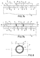
- the device 60 comprises a plate 62 having holes suction 64 opening on one side of the plate into an enclosure 66 in air depression Dp in relation to the ambient environment and on the other side of the plate, in a foreground P1, in the ambient environment.
- the alumina-bearing substrate 44 is placed by its first face 51 on the foreground P1, on the other side of the plate 62, at the pressure ambient, on the suction holes 64.
- the carrier substrate is maintained applied against the plate by the depression Dp through the holes 64.
- the ferrite substrate 46 is placed in succession in the recess 50 of the carrier substrate, its first face 53 being applied against the plate 62 on the foreground P1.
- the ferrite substrate is in turn maintained in position against the plate by the depression Dp through the holes 64
- the two substrates having the same thickness, the second face 52 of the carrier substrate and the second face 54 of the ferrite substrate are located on the same second plane P2 represents in FIG. 7b.
- a gap 68 appears between the carrier substrate alumina 44 and the ferrite substrate 46 positioned in the recess 50.
- a dielectric sealing paste 70 for example glass of sealing, is then deposited in the gap 68 using a screen serigraph 72
- the sealing compound must have a coefficient of expansion K compatible with the coefficient of expansion K1 of the carrier substrate and the coefficient of expansion K2 of the ferrite substrate.
- fixing the substrate ferrite 46 to the carrier substrate 44 by the dielectric sealing glass is obtained by baking at about a temperature of 850 ° C, forming the single substrate 42.
- Figure 9a shows a section of the single substrate 42 after metallization and FIG. 9b a view of one of its metallized faces.
- Metallizations 80 are deposited on both sides of the single substrate 42 thus achieving in a single operation the metallization of the alumina carrier substrate 44, ferrite substrate 46 and the metallizations of the sealing glass 70 located at the gap 68.
- An industrial gain is also obtained on the cost of production of the module by the reduction in the cost linked to the manufacture of the single substrate and the simplification of its mounting in the module housing.
- the cycle of module manufacturing can be lowered by at least an hour thanks to the elimination of the manual operation of mounting the ferrite substrate in the housing and the elimination of the wired wiring of the modules of the prior art.
- micro-electronic module shown in example in Figure 4 is not limiting. More complex modules using a carrier substrate and several ferrite substrates sealed in the carrier substrate according to the invention, in order to produce circulators or insulators microwaves can integrate passive elements produced by thick film techniques, for example screen-printed resistors from a paste made from Rhutenium dioxide, but also from chips and integrated circuits transferred onto the substrate according to known techniques.
- micro-electronic modules according to the invention provides better stability of the module's microwave performance and very good resistance to rapid temperature variations which can be between approximately -55 ° C and + 125 ° C,
Abstract
Description
La présente invention concerne les modules micro-électroniques hyperfréquences comportant deux matériaux de substrat différents dans une structure d'interconnexion en couche épaisse. L'invention concerne aussi le procédé de fabrication d'un tel module et plus précisément la fabrication du substrat métallisé du module.The present invention relates to micro-electronic modules microwave with two different substrate materials in one thick layer interconnection structure. The invention also relates to method of manufacturing such a module and more precisely the manufacture of metallized substrate of the module.
Les modules micro-électroniques modernes permettent de réaliser des fonctions électroniques diverses en associant sur un substrat des composants variés comme des résistances, des condensateurs, des diodes, des transistors, des circuits intégrés hyperfréquences etc. Le substrat peut être de type céramique ou verre et comporte les liaisons électriques et tout ou partie des composants passifs réalisés par exemple par des techniques de couche épaisse.Modern micro-electronic modules allow perform various electronic functions by combining on a substrate various components such as resistors, capacitors, diodes, transistors, microwave integrated circuits etc. The substrate can be of ceramic or glass type and has the connections electrical and all or part of the passive components produced for example by thick layer techniques.
Dans certaines applications en hyperfréquence, ces modules micro-électroniques utilisent dans une technologie microbande fonctionnant jusqu'à 20 GHz, deux substrats réalisés dans des matériaux différents, généralement un substrat d'alumine (Al2O3) de pureté 99.6% et un substrat ferrite.In certain microwave applications, these microelectronic modules use in a microstrip technology operating up to 20 GHz, two substrates made of different materials, generally an alumina substrate (Al 2 O 3 ) of 99.6% purity and a substrate ferrite.
Le substrat d'alumine (Al2O3) reçoit les fonctions de type oscillateur, amplificateur, filtre, le substrat ferrite recevant les fonctions isolateur, circulateur.The alumina substrate (Al 2 O 3 ) receives the functions of oscillator, amplifier, filter type, the ferrite substrate receiving the functions of isolator, circulator.
Ces deux types de substrat sont manufactures séparément en utilisant des moyens d'usinage laser et sérigraphie couche épaisse pour les fonctions précédemment citées.These two types of substrate are manufactured separately in using laser machining means and thick layer screen printing for previously mentioned functions.
La figure 1 montre un module micro-électronique 10
hyperfréquences selon l'art antérieur comportant deux substrats en
matériaux différents, un substrat d'alumine 12 (ou substrat porteur en
alumine) et un substrat ferrite 14, intégrés dans un boítier 16 en titane. Le
substrat en alumine 12 comporte des métallisations 18 sur chacune des ses
deux faces opposées, et de la même façon le substrat ferrite comporte des
métallisations 20. Les métallisations des deux substrats sont réalisées en
technologie couche épaisse. Figure 1 shows a
Selon l'art antérieur, dans une première phase, les deux substrats métallisés sont réalisés séparément selon des techniques connues.According to the prior art, in a first phase, the two substrates metallized are produced separately according to known techniques.
La figure 2a montre le substrat en alumine 12 dans lequel est
effectué un passage 30 de forme circulaire par découpe au laser CO2 afin
de recevoir le substrat ferrite 14 en forme de plaquette circulaire de
dimension sensiblement identique à celle du passage 30. Les tolérances de
fabrications du passage 30 et du substrat ferrite 14 sont telles que le
substrat 14 puisse être inséré dans le passage 30 sans difficulté. La figure
2b représente une vue en coupe, selon un axe AA', montrant le passage 30
du substrat en alumine de la figure 2a.FIG. 2a shows the
La figure 3a montre le substrat ferrite 14 comportant les
métallisations 20. La figure 3b représente une vue en coupe selon un axe
BB' du substrat ferrite de la figure 3a.FIG. 3a shows the
Dans une seconde phase de la fabrication du module, on effectue l'intégration du substrat en alumine 12 métallisé et du substrat ferrite 14 métallisé dans le boítier 16 du module micro-électronique 10 représenté à la figure 1. Cette intégration comporte au moins les opérations suivantes.
- collage du substrat d'alumine 12 dans le
boítier 16 par unfilm 22 tramé conducteur électrique préimpreigné de colle conductrice, puis polymérisation à chaud de la colle rendant le substrat enalumine 12 solidaire duboítier 16. - collage du substrat ferrite 14 avec de la colle conductrice 24
dans le fond du
boítier 16, le substrat ferrite 14 étant positionné préalablement à la main à l'intérieur de l'évidement 30 du substrat enalumine 12.
- bonding of the
alumina substrate 12 in thehousing 16 by a screened electricallyconductive film 22 pre-impregnated with conductive adhesive, then hot polymerization of the adhesive making thealumina substrate 12 integral with thehousing 16. - bonding of the
ferrite substrate 14 withconductive adhesive 24 in the bottom of thehousing 16, theferrite substrate 14 being positioned beforehand by hand inside therecess 30 of thealumina substrate 12.
Le positionnement du substrat ferrite 14 dans le boítier 16, à l'intérieur du passage 30 du substrat en alumine, est effectué en utilisant trois rondins de calibration (non représentés à la figure 1) placés entre le substrat ferrite 14 et le fond du boítier 16, d'une part afin d'éviter la remontée de colle dans un interstice 26 apparaissant entre le substrat ferrite 14 et le substrat d'alumine 12 et d'autre part pour mettre au même niveau le substrat ferrite 14 et le substrat en alumine 12.
- réalisation des interconnexions électriques entre les
métallisations 18 du substrat enalumine 12 et lesmétallisations 20 du substrat ferrite 14 par microcâblage defils 32 en or d'un diamètre d'environ 25 micromètres. Le microcâblage desfils 32 est réalisé par ultrasons, thermo-compression ou soudure électrique.
- making electrical interconnections between the
metallizations 18 of thealumina substrate 12 and themetallizations 20 of theferrite substrate 14 by micro-wiring ofgold wires 32 with a diameter of about 25 micrometers. The micro-wiring of thewires 32 is carried out by ultrasound, thermo-compression or electrical welding.
Un petit aimant permanent, non représente sur la figure 1, est disposé sur le substrat ferrite d'une façon connue afin de réaliser la fonction d'isolateur ou de circulateur nécessaire au fonctionnement du module micro-électronique de la figure 1.A small permanent magnet, not shown in Figure 1, is arranged on the ferrite substrate in a known manner in order to perform the function isolator or circulator necessary for the operation of the microelectronic module of figure 1.
Le module micro-électronique peut être plus complexe que celui représente en exemple à la figure 1 pouvant comporter plusieurs substrats ferrites. En général, dans les modules micro-électroniques actuels, on trouve un substrat d'alumine et 3 à 5 substrats ferrites.The microelectronic module can be more complex than that represents in example in FIG. 1 which can comprise several substrates ferrites. In general, in current micro-electronic modules, we find an alumina substrate and 3 to 5 ferrite substrates.
La fabrication des modules micro-électroniques hyperfréquences selon l'art antérieur comporte deux opérations de sérigraphie séparées pour la réalisation des métallisations des substrats en matériaux différents et implique un microcâblage filaire des interconnexions électriques entre ces substrats, long et délicat et par conséquent coûteux.The manufacturing of microwave micro-electronic modules according to the prior art comprises two separate screen printing operations for the metallization of substrates in different materials and involves wired micro-wiring of the electrical interconnections between these substrates, long and delicate and therefore expensive.
La présente invention permet de résoudre le double problème de sérigraphie séparée des substrats en matériaux différents et d'interconnexion par microcâblage filaire entre les substrats en proposant un module micro-électronique hyperfréquences comportant un substrat porteur et un substrat ferrite séparés par un interstice, chaque substrat ayant au moins une face métallisée, une première face métallisée du substrat porteur et une première face métallisée du substrat ferrite étant situées dans un même premier plan, les deux substrats étant situés d'un même coté de ce premier plan, caractérisé en ce que le substrat ferrite est fixé au substrat porteur par une matière située dans l'interstice et qui affleure dans le premier plan, le substrat porteur, le substrat ferrite et la matière, formant un substrat unique métallisé, la matière là où elle affleure dans le premier plan étant recouverte par une métallisation assurant l'interconnexion électrique entre celles des faces métallisées du substrat porteur et du substrat ferrite qui sont situées dans le premier plan.The present invention solves the double problem of separate screen printing of substrates made of different materials and interconnection by wire micro-wiring between the substrates by proposing a microwave micro-electronic module comprising a carrier substrate and a ferrite substrate separated by a gap, each substrate having at at least one metallized face, a first metallized face of the carrier substrate and a first metallized face of the ferrite substrate being located in a same foreground, the two substrates being located on the same side of this foreground, characterized in that the ferrite substrate is fixed to the substrate carrier by a material located in the gap and which outcrops in the foreground, the carrier substrate, the ferrite substrate and the material, forming a unique metallized substrate, the material where it is exposed in the foreground being covered by a metallization ensuring electrical interconnection between those of the metallized faces of the carrier substrate and the ferrite substrate which are located in the foreground.
Dans une réalisation du module micro-électronique selon l'invention, le substrat porteur et le substrat ferrite sont de même épaisseur et comportent chacun une seconde face métallisée, respectivement une seconde face métallisée du substrat porteur et une seconde face métallisée du substrat ferrite. Ces secondes faces métallisées sont situées dans un même second plan, et la matière située dans l'interstice et qui affleure dans le second plan est recouverte par une métallisation située dans ce second plan assurant l'interconnexion électrique entre celles des faces métallisées du substrat porteur et du substrat ferrite qui sont situées dans le second plan. Dans cette réalisation le substrat unique comporte des métallisations sur ses deux faces situées respectivement sur le premier et le second plan.In an embodiment of the microelectronic module according to the invention, the carrier substrate and the ferrite substrate are of the same thickness and each have a second metallized face, respectively a second metallized face of the carrier substrate and a second metallized face of ferrite substrate. These second metallized faces are located in a same background, and the material located in the interstice and which is exposed in the second plane is covered by a metallization located in this second plan ensuring the electrical interconnection between those of the metallized faces of the carrier substrate and the ferrite substrate which are located in the second plan. In this embodiment the single substrate includes metallizations on its two faces located respectively on the first and the second plane.
Dans les réalisations du module selon l'invention, la matière située dans l'interstice est une pâte de scellement diélectrique, par exemple un verre de scellement diélectrique. Cette pâte doit présenter un coefficient de dilatation K compatible, c'est-à-dire de valeur proche et de même signe, que les coefficients de dilatation K1 du substrat porteur et K2 du substrat ferrite, afin d'obtenir une fixation fiable du substrat ferrite au substrat porteur.In the embodiments of the module according to the invention, the material located in the gap is a dielectric sealing paste, for example a dielectric sealing glass. This dough must have a coefficient of compatible K dilation, that is to say of close value and of the same sign, that the expansion coefficients K1 of the carrier substrate and K2 of the substrate ferrite, in order to obtain a reliable fixing of the ferrite substrate to the substrate carrier.
La présente invention proposé aussi un procédé de fabrication d'un tel module micro-électronique hyperfréquences selon l'invention, caractérisé en ce qu'il comporte au moins les étapes suivantes:
- réalisation du substrat porteur et du substrat ferrite.
- production of the carrier substrate and the ferrite substrate.
Dans cette étape de fabrication le substrat porteur et le substrat ferrite ne sont pas encore métallisés
- fixation du substrat ferrite au substrat porteur par une matière remplissant l'interstice entre le substrat porteur et le substrat ferrite, la première face du substrat porteur et la première face du substrat ferrite étant situées dans le même premier plan, les deux substrats étant situés d'un même coté du premier plan.
- métallisation d'au moins la face du substrat unique située dans le premier plan.
- fixing the ferrite substrate to the carrier substrate by a material filling the gap between the carrier substrate and the ferrite substrate, the first face of the carrier substrate and the first face of the ferrite substrate being located in the same first plane, the two substrates being located d 'same side of the foreground.
- metallization of at least the face of the single substrate located in the foreground.
La fabrication selon l'invention d'un substrat unique métallisé permet de supprimer au moins deux opérations importantes et coûteuse nécessaires dans les procédés de fabrication de l'art antérieur, le collage du substrat ferrite dans le boítier du module et l'interconnexion par microcâblage filaire entre les métallisations des deux substrats.The production according to the invention of a single metallized substrate eliminates at least two important and costly operations necessary in the manufacturing processes of the prior art, the bonding of the ferrite substrate in the module housing and interconnection by wire micro-wiring between the metallizations of the two substrates.
En effet l'intégration dans le boítier du module micro-électronique du substrat unique constitué par le substrat porteur le substrat ferrite et la matière de remplissage de l'interstice entre les deux substrat est réalisé en une seule opération contrairement au procédé de fabrication selon l'art antérieur qui nécessite comme décrit précédemment au moins deux opérations, une pour chacun des substrats, consistant en une première opération d'intégration dans le boítier du substrat en alumine métallisé puis une seconde opération intégration dans le boítier du substrat ferrite métallisé.Indeed the integration in the housing of the micro-electronic module of the single substrate constituted by the carrier substrate the ferrite substrate and the filling material of the gap between the two substrates is made of a single operation unlike the manufacturing process according to art previous which requires as described above at least two operations, one for each of the substrates, consisting of a first integration operation in the housing of the metallized alumina substrate then a second integration operation in the housing of the ferrite substrate metallic.
Un autre avantage du procédé de fabrication du module selon l'invention réside dans la seule opération de métallisation du substrat unique et la suppression du microcâblage filaire nécessaire dans la fabrication des modules selon l'art antérieur. En effet une seule opération de métallisation collective en couche épaisse du substrat unique permet de réaliser les métallisations du substrat porteur, du substrat ferrite fixé au substrat porteur et de la matière située dans l'interstice affleurant au niveau des faces du substrat unique, ce qui assure l'interconnexion électrique entre les métallisations du substrat porteur et celles du substrat ferrite.Another advantage of the module manufacturing process according to the invention lies in the sole metallization operation of the substrate and the removal of the wired micro-wiring required in the manufacture of modules according to the prior art. Indeed only one operation collective metallization in a thick layer of the single substrate allows metallizing the carrier substrate, the ferrite substrate attached to the carrier substrate and material located in the gap flush with the level faces of the single substrate, which ensures electrical interconnection between the metallizations of the carrier substrate and those of the ferrite substrate.
D'autres caractéristiques et avantages de l'invention apparaítront à la lecture de la description détaillée qui en est faite en référence aux dessins annexés dans lesquels :
- la figure 1 représente un module micro-électronique, déjà décrit, selon l'art antérieur.
- les figures 2a,2b,3a,3b des vues du substrat d'alumine et du substrat ferrite du module de la figure 1, selon l'art antérieur.
- la figure 4 représente un module micro-électronique selon l'invention.
- les figures 5a,5b,6a,6b, des vues du substrat en porteur et du substrat ferrite du module de la figure 4 selon l'invention.
- les figures 7a et 7b montrent un dispositif utilisé pour la fixation du substrat ferrite au substrat porteur.
- la figure 8 montre le substrat unique du module de la figure 4 selon l'invention.
- les figures 9a et 9b montrent le substrat unique métallisé du module de la figure 4 selon l'invention.
- FIG. 1 represents a microelectronic module, already described, according to the prior art.
- Figures 2a, 2b, 3a, 3b views of the alumina substrate and the ferrite substrate of the module of Figure 1, according to the prior art.
- FIG. 4 represents a microelectronic module according to the invention.
- Figures 5a, 5b, 6a, 6b, views of the carrier substrate and the ferrite substrate of the module of Figure 4 according to the invention.
- Figures 7a and 7b show a device used for fixing the ferrite substrate to the carrier substrate.
- Figure 8 shows the single substrate of the module of Figure 4 according to the invention.
- Figures 9a and 9b show the single metallized substrate of the module of Figure 4 according to the invention.
La figure 4 représente un module électronique 40 selon l'invention
comportant un substrat unique 42 métallisé sur ses deux faces et réalisé à
partir d'un substrat porteur en alumine 44 et un substrat ferrite 46 intégré ou
scellé au substrat porteur dans un évidement 50 circulaire réalisé dans le
substrat porteur en alumine, le substrat porteur et le substrat ferrite ayant
sensiblement la même épaisseur.FIG. 4 represents an
Chaque substrat comporte une première face et une seconde face
opposée à la première, respectivement une première face 51 et une
seconde face 52 du substrat porteur et une première face 53 et une seconde
face 54 du substrat ferrite.Each substrate has a first side and a second side
opposite the first, respectively a
Le procédé de fabrication du module micro-électronique 40 comporte au moins les étapes de fabrication suivantes décrites en référence aux figures 4,5a,5b,6a,6b,7a,7b,8,9a et 9b.
- réalisation du substrat porteur en alumine 44 selon des
techniques connues,
comportant un passage 50 de forme circulaire permettant le scellement du substrat ferrite 46 dans le substrat porteur en alumine 44.Le passage 50 peut être réalisé par une découpe au laser C02 du substrat porteur.
- production of the
alumina carrier substrate 44 according to known techniques, comprising apassage 50 of circular shape allowing the sealing of theferrite substrate 46 in thealumina carrier substrate 44. Thepassage 50 can be produced by laser cutting C02 of the carrier substrate.
La figure 5a montre une vue partielle du substrat porteur et la figure 5b une coupe dans un plan perpendiculaire à la surface circulaire du substrat porteur selon un axe CC' montrant le passage 50.
- réalisation du substrat ferrite 46 en forme de pastille circulaire de
diamètre sensiblement identique à celui du
passage 50. Les tolérances de fabrications dupassage 50 et du substrat ferrite 46 sont telles que ce dernier puisse être inséré dans lepassage 50 sans difficulté. Par exemple dans cette réalisation les tolérances sur le diamètre de découpe du passage circulaire dans le substrat porteur sont de 0µm, +20µm et les tolérances sur le diamètre du substrat ferrite sont de 0µm, -20µm.
- production of the
ferrite substrate 46 in the form of a circular pellet with a diameter substantially identical to that of thepassage 50. The manufacturing tolerances of thepassage 50 and of theferrite substrate 46 are such that the latter can be inserted into thepassage 50 without difficulty. For example, in this embodiment, the tolerances on the cutting diameter of the circular passage in the carrier substrate are 0 μm, + 20 μm and the tolerances on the diameter of the ferrite substrate are 0 μm, -20 μm.
Les figures 6a et 6b montrent une vue du substrat ferrite 46 et une coupe dans un plan perpendiculaire à la surface circulaire du substrat ferrite selon un axe DD'.
- fixation du substrat ferrite 46 dans le substrat porteur 44 en
alumine. A cet effet on utilise
un dispositif 60 représenté aux figures 7a et 7b.
- fixing the
ferrite substrate 46 in thecarrier substrate 44 in alumina. To this end, adevice 60 shown in FIGS. 7a and 7b is used.
Le dispositif 60 comporte une plaque 62 ayant des trous
d'aspiration 64 débouchant d'un côté de la plaque dans une enceinte 66 en
dépression d'air Dp par rapport au milieu ambiant et de l'autre côté de la
plaque, dans un premier plan P1, dans le milieu ambiant. The
Le substrat porteur en alumine 44 est posé par sa première face
51 sur le premier plan P1, de l'autre côté de la plaque 62, à la pression
ambiante, sur les trous d'aspiration 64. Le substrat porteur est maintenu
appliqué contre la plaque par la dépression Dp à travers les trous 64.The alumina-bearing
Le substrat en ferrite 46 est placé en suite dans l'évidement 50 du
substrat porteur, sa première face 53 étant appliquée contre la plaque 62 sur
le premier plan P1. Le substrat ferrite se trouve à son tour maintenu en
position contre la plaque par la dépression Dp à travers les trous 64The
Les deux substrats ayant la même épaisseur, la seconde face 52
du substrat porteur et la seconde face 54 du substrat ferrite se trouvent
situées sur un même second plan P2 représente à la figure 7b.The two substrates having the same thickness, the
Un interstice 68 apparaít entre le substrat porteur en alumine 44
et le substrat ferrite 46 positionné dans l'évidement 50.A
Une pâte de scellement 70 diélectrique, par exemple du verre de
scellement, est alors déposée dans l'interstice 68 à l'aide d'un écran de
sérigraphie 72A dielectric sealing
La pâte de scellement doit présenter un coefficient de dilatation K compatible avec le coefficient de dilatation K1 du substrat porteur et le coefficient de dilatation K2 du substrat ferrite.The sealing compound must have a coefficient of expansion K compatible with the coefficient of expansion K1 of the carrier substrate and the coefficient of expansion K2 of the ferrite substrate.
Dans le cas de la réalisation du substrat unique 42 du module de
la figure 4:
Après séchage du verre de scellement, la fixation du substrat
ferrite 46 au substrat porteur 44 par le verre de scellement diélectrique est
obtenu, par une cuisson à environ une température de 850°C, formant le
substrat unique 42.After drying the sealing glass, fixing the
Le substrat ferrite 46 devenant solidaire du substrat porteur 44, le substrat unique 42 pourra être métallisé.
- métallisation du substrat unique 42 selon les techniques connues en couche épaisse.
- metallization of the
single substrate 42 according to known techniques in a thick layer.
La figure 9a montre une coupe du substrat unique 42 après
métallisation et la figure 9b une vue d'une de ses faces métallisée.Figure 9a shows a section of the
Des métallisations 80 sont déposées sur les deux faces du
substrat unique 42 réalisant ainsi en une seule opération la métallisation du
substrat porteur en alumine 44, du substrat ferrite 46 ainsi que les
métallisations du verre de scellement 70 situées au niveau de l'interstice 68.
Les metallisations 80 du substrat unique comportent une première zone de métallisation 76 situé sur une des faces du substrat unique, assurant l'interconnexion électrique entre les métallisations des premières faces 51,53 des deux substrats et une seconde zone de metallisation 74 située sur l'autre face du substrat unique assurant l'interconnexion électrique entre les métallisations des secondes faces 52,54 des deux mêmes substrats.
- fixation du substrat unique métallisé selon des méthodes connues dans le boítier 16, par exemple par collage par un film tramé conducteur électrique préimpregné de colle conductrice.
- fixing the single metallized substrate according to methods known in the
housing 16, for example by bonding with an electrically conductive screened film pre-impregnated with conductive adhesive.
La métallisation collective du substrat unique en évitant l'interconnexion filaire de 25 micromètres, assure une meilleure reproductibilité des performances hyperfréquences du module ainsi réalisé.Collective metallization of the single substrate avoiding 25 micrometer wired interconnection, ensures better reproducibility of the microwave performance of the module thus produced.
On obtient également un gain industriel sur le coût de réalisation du module par la diminution du coût liée à la fabrication du substrat unique et la simplification de son montage dans le boítier du module. Le cycle de fabrication du module peut être baissé d'au moins une heure grâce à la suppression de l'opération manuelle de montage du substrat ferrite dans le boítier et la suppression du câblage filaire des modules de l'art antérieur.An industrial gain is also obtained on the cost of production of the module by the reduction in the cost linked to the manufacture of the single substrate and the simplification of its mounting in the module housing. The cycle of module manufacturing can be lowered by at least an hour thanks to the elimination of the manual operation of mounting the ferrite substrate in the housing and the elimination of the wired wiring of the modules of the prior art.
La réalisation du module micro-électronique montrée en exemple dans la figure 4 n'est pas limitative. Des modules plus complexes utilisant un substrat porteur et plusieurs substrats ferrite scellés dans le substrat porteur selon l'invention, afin de réaliser des circulateurs ou des isolateurs hyperfréquences peuvent intégrer des éléments passifs réalisés par des techniques en couches épaisses, par exemple des résistances sérigraphiées à partir d'une pâte en dioxyde de Rhutenium, mais aussi des puces et des circuits intégrés reportés sur le substrat selon les techniques connues.The realization of the micro-electronic module shown in example in Figure 4 is not limiting. More complex modules using a carrier substrate and several ferrite substrates sealed in the carrier substrate according to the invention, in order to produce circulators or insulators microwaves can integrate passive elements produced by thick film techniques, for example screen-printed resistors from a paste made from Rhutenium dioxide, but also from chips and integrated circuits transferred onto the substrate according to known techniques.
La réalisation des modules micro-électroniques selon l'invention assure une meilleur stabilité des performances hyperfréquences du module et une très bonne tenue aux variation rapides en température qui peut être comprise entre environ -55°C et +125°C,The realization of the micro-electronic modules according to the invention provides better stability of the module's microwave performance and very good resistance to rapid temperature variations which can be between approximately -55 ° C and + 125 ° C,
Claims (12)
Applications Claiming Priority (2)
| Application Number | Priority Date | Filing Date | Title |
|---|---|---|---|
| FR9807096A FR2779576B1 (en) | 1998-06-05 | 1998-06-05 | MICRO-ELECTRONIC MICRO-ELECTRONIC MODULE COMPRISING TWO DIFFERENT SUBSTRATE MATERIALS AND METHOD FOR MANUFACTURING SUCH A MODULE |
| FR9807096 | 1998-06-05 |
Publications (2)
| Publication Number | Publication Date |
|---|---|
| EP0962980A1 true EP0962980A1 (en) | 1999-12-08 |
| EP0962980B1 EP0962980B1 (en) | 2006-12-27 |
Family
ID=9527062
Family Applications (1)
| Application Number | Title | Priority Date | Filing Date |
|---|---|---|---|
| EP99401359A Expired - Lifetime EP0962980B1 (en) | 1998-06-05 | 1999-06-04 | Microelectronic hyperfrequency module having two different substrate materials and method of making such module |
Country Status (4)
| Country | Link |
|---|---|
| EP (1) | EP0962980B1 (en) |
| DE (1) | DE69934542T2 (en) |
| ES (1) | ES2280114T3 (en) |
| FR (1) | FR2779576B1 (en) |
Cited By (1)
| Publication number | Priority date | Publication date | Assignee | Title |
|---|---|---|---|---|
| WO2002043146A1 (en) * | 2000-11-21 | 2002-05-30 | Kerafol Keramische Folien Gmbh | Ferrite film |
Citations (2)
| Publication number | Priority date | Publication date | Assignee | Title |
|---|---|---|---|---|
| EP0197476A2 (en) * | 1985-04-03 | 1986-10-15 | ANT Nachrichtentechnik GmbH | Microwave circulator |
| US5745981A (en) * | 1993-04-01 | 1998-05-05 | General Electric Company | Method for making magnetic and electromagnetic circuit components having embedded magnetic materials in a high density interconnect structure |
-
1998
- 1998-06-05 FR FR9807096A patent/FR2779576B1/en not_active Expired - Fee Related
-
1999
- 1999-06-04 EP EP99401359A patent/EP0962980B1/en not_active Expired - Lifetime
- 1999-06-04 ES ES99401359T patent/ES2280114T3/en not_active Expired - Lifetime
- 1999-06-04 DE DE69934542T patent/DE69934542T2/en not_active Expired - Lifetime
Patent Citations (2)
| Publication number | Priority date | Publication date | Assignee | Title |
|---|---|---|---|---|
| EP0197476A2 (en) * | 1985-04-03 | 1986-10-15 | ANT Nachrichtentechnik GmbH | Microwave circulator |
| US5745981A (en) * | 1993-04-01 | 1998-05-05 | General Electric Company | Method for making magnetic and electromagnetic circuit components having embedded magnetic materials in a high density interconnect structure |
Non-Patent Citations (1)
| Title |
|---|
| H. TOMIMURO ET AL.: "Reliability study on microwave integrated circuits for the 20G-D2 transmission systems", REVIEW OF THE ELECTRICAL COMMUNICATION LABORATORIES, vol. 32, no. 6, November 1984 (1984-11-01), tokyo,JP, pages 1100 - 1106, XP002093322 * |
Cited By (1)
| Publication number | Priority date | Publication date | Assignee | Title |
|---|---|---|---|---|
| WO2002043146A1 (en) * | 2000-11-21 | 2002-05-30 | Kerafol Keramische Folien Gmbh | Ferrite film |
Also Published As
| Publication number | Publication date |
|---|---|
| DE69934542D1 (en) | 2007-02-08 |
| FR2779576A1 (en) | 1999-12-10 |
| EP0962980B1 (en) | 2006-12-27 |
| ES2280114T3 (en) | 2007-09-01 |
| FR2779576B1 (en) | 2001-04-27 |
| DE69934542T2 (en) | 2007-10-25 |
Similar Documents
| Publication | Publication Date | Title |
|---|---|---|
| EP1053592B1 (en) | Encapsulated surface wave component and collective method for making same | |
| US7692292B2 (en) | Packaged electronic element and method of producing electronic element package | |
| EP0638933B1 (en) | Interconnection process of stacked semi-conductors chips and devices | |
| CA2321360C (en) | Process for encapsulating electronic components | |
| EP3089211B1 (en) | Method for packaging an electronic circuit | |
| EP1964204B1 (en) | Module with frequency-tunable function | |
| EP1657749B1 (en) | Multilevel microelectronic package with internal shielding | |
| EP1557394B1 (en) | Apparatus and method for securing hermeticity of a cavity in which a passage ends | |
| FR2635920A1 (en) | METHOD FOR MANUFACTURING A CONNECTION ZONE FOR A TRIPLATE-TYPE MICROWAVE CIRCUIT AND CIRCUIT THUS OBTAINED | |
| EP0962980A1 (en) | Microelectronic hyperfrequency module having two different substrate materials and method of making such module | |
| FR2565030A1 (en) | STRUCTURE OF CONTACTING RESET METALLIZATIONS OF A SEMICONDUCTOR DEVICE AND DEVICE HAVING SUCH A STRUCTURE | |
| FR3098646A1 (en) | ELECTRONIC COMPONENT RESISTANT TO HUMIDITY AND METHOD FOR MAKING SUCH A COMPONENT | |
| CA2915856A1 (en) | Differential temperature sensor | |
| FR2598032A1 (en) | HYBRID INTEGRATED CIRCUIT FOR ISOLATION AMPLIFIER | |
| FR2529386A1 (en) | Electronic circuit casing with multilayer capacitor - has base and hood with reactor realised on hood surface or within its thickness | |
| FR2529385A1 (en) | MICROBOITIER FOR ENCAPSULATION OF LOGIC INTEGRATED CIRCUITS OPERATING IN VERY HIGH FREQUENCY | |
| FR2489592A1 (en) | CERAMIC MICRO-BOX FOR ELECTRONIC CIRCUIT ENCAPSULATION | |
| FR2554275A1 (en) | Connection device for a power semiconductor | |
| FR2633789A1 (en) | COMPACT FILTER WITH RESONATORS USING THE PIEZOELECTRIC EFFECT | |
| EP2197029B1 (en) | Microwave frequency integrated circuit encapsulated in a housing | |
| FR2507017A1 (en) | Microcircuit assembly for multistage microwave TV signal amplifier - comprises silicon base covered by insulating layer and supporting transistor chips interconnected by lines formed by metallisations | |
| FR2674682A1 (en) | HYBRID MODULE AND PRODUCTION METHOD. | |
| FR3083955A1 (en) | METHOD FOR MANUFACTURING AN ELECTRONIC POWER MODULE FOR ELECTRONICS ON BOARD ON AN AIRCRAFT | |
| FR3136588A1 (en) | HOUSING, FOR EXAMPLE OPTICAL BOX, OF INTEGRATED CIRCUIT | |
| FR2843485A1 (en) | Fabrication of a module of integrated circuits with a substrate and a number of components using a support for the components and forming the substrate above them with the incorporation of a metal layer |
Legal Events
| Date | Code | Title | Description |
|---|---|---|---|
| PUAI | Public reference made under article 153(3) epc to a published international application that has entered the european phase |
Free format text: ORIGINAL CODE: 0009012 |
|
| AK | Designated contracting states |
Kind code of ref document: A1 Designated state(s): DE ES FI FR GB GR IT SE |
|
| AX | Request for extension of the european patent |
Free format text: AL;LT;LV;MK;RO;SI |
|
| 17P | Request for examination filed |
Effective date: 20000412 |
|
| AKX | Designation fees paid |
Free format text: DE ES FI FR GB GR IT SE |
|
| RAP1 | Party data changed (applicant data changed or rights of an application transferred) |
Owner name: THALES |
|
| GRAP | Despatch of communication of intention to grant a patent |
Free format text: ORIGINAL CODE: EPIDOSNIGR1 |
|
| GRAS | Grant fee paid |
Free format text: ORIGINAL CODE: EPIDOSNIGR3 |
|
| GRAA | (expected) grant |
Free format text: ORIGINAL CODE: 0009210 |
|
| AK | Designated contracting states |
Kind code of ref document: B1 Designated state(s): DE ES FI FR GB GR IT SE |
|
| REG | Reference to a national code |
Ref country code: GB Ref legal event code: FG4D Free format text: NOT ENGLISH |
|
| REF | Corresponds to: |
Ref document number: 69934542 Country of ref document: DE Date of ref document: 20070208 Kind code of ref document: P |
|
| REG | Reference to a national code |
Ref country code: SE Ref legal event code: TRGR |
|
| REG | Reference to a national code |
Ref country code: GR Ref legal event code: EP Ref document number: 20070400947 Country of ref document: GR |
|
| REG | Reference to a national code |
Ref country code: ES Ref legal event code: FG2A Ref document number: 2280114 Country of ref document: ES Kind code of ref document: T3 |
|
| PLBE | No opposition filed within time limit |
Free format text: ORIGINAL CODE: 0009261 |
|
| STAA | Information on the status of an ep patent application or granted ep patent |
Free format text: STATUS: NO OPPOSITION FILED WITHIN TIME LIMIT |
|
| 26N | No opposition filed |
Effective date: 20070928 |
|
| REG | Reference to a national code |
Ref country code: FR Ref legal event code: PLFP Year of fee payment: 17 |
|
| PGFP | Annual fee paid to national office [announced via postgrant information from national office to epo] |
Ref country code: GB Payment date: 20150603 Year of fee payment: 17 Ref country code: DE Payment date: 20150527 Year of fee payment: 17 Ref country code: ES Payment date: 20150527 Year of fee payment: 17 Ref country code: FI Payment date: 20150609 Year of fee payment: 17 Ref country code: SE Payment date: 20150611 Year of fee payment: 17 |
|
| PGFP | Annual fee paid to national office [announced via postgrant information from national office to epo] |
Ref country code: GR Payment date: 20150529 Year of fee payment: 17 Ref country code: FR Payment date: 20150608 Year of fee payment: 17 |
|
| PGFP | Annual fee paid to national office [announced via postgrant information from national office to epo] |
Ref country code: IT Payment date: 20150625 Year of fee payment: 17 |
|
| REG | Reference to a national code |
Ref country code: DE Ref legal event code: R119 Ref document number: 69934542 Country of ref document: DE |
|
| PG25 | Lapsed in a contracting state [announced via postgrant information from national office to epo] |
Ref country code: FI Free format text: LAPSE BECAUSE OF NON-PAYMENT OF DUE FEES Effective date: 20160604 |
|
| REG | Reference to a national code |
Ref country code: SE Ref legal event code: EUG |
|
| PG25 | Lapsed in a contracting state [announced via postgrant information from national office to epo] |
Ref country code: SE Free format text: LAPSE BECAUSE OF NON-PAYMENT OF DUE FEES Effective date: 20160605 |
|
| GBPC | Gb: european patent ceased through non-payment of renewal fee |
Effective date: 20160604 |
|
| REG | Reference to a national code |
Ref country code: GR Ref legal event code: ML Ref document number: 20070400947 Country of ref document: GR Effective date: 20170109 |
|
| REG | Reference to a national code |
Ref country code: FR Ref legal event code: ST Effective date: 20170228 |
|
| PG25 | Lapsed in a contracting state [announced via postgrant information from national office to epo] |
Ref country code: FR Free format text: LAPSE BECAUSE OF NON-PAYMENT OF DUE FEES Effective date: 20160630 Ref country code: DE Free format text: LAPSE BECAUSE OF NON-PAYMENT OF DUE FEES Effective date: 20170103 Ref country code: GR Free format text: LAPSE BECAUSE OF NON-PAYMENT OF DUE FEES Effective date: 20170109 |
|
| PG25 | Lapsed in a contracting state [announced via postgrant information from national office to epo] |
Ref country code: GB Free format text: LAPSE BECAUSE OF NON-PAYMENT OF DUE FEES Effective date: 20160604 |
|
| PG25 | Lapsed in a contracting state [announced via postgrant information from national office to epo] |
Ref country code: IT Free format text: LAPSE BECAUSE OF NON-PAYMENT OF DUE FEES Effective date: 20160604 |
|
| REG | Reference to a national code |
Ref country code: ES Ref legal event code: FD2A Effective date: 20180507 |
|
| PG25 | Lapsed in a contracting state [announced via postgrant information from national office to epo] |
Ref country code: ES Free format text: LAPSE BECAUSE OF NON-PAYMENT OF DUE FEES Effective date: 20160605 |