EP0961311A2 - Capacitor and method for fabricating the same - Google Patents
Capacitor and method for fabricating the same Download PDFInfo
- Publication number
- EP0961311A2 EP0961311A2 EP99110230A EP99110230A EP0961311A2 EP 0961311 A2 EP0961311 A2 EP 0961311A2 EP 99110230 A EP99110230 A EP 99110230A EP 99110230 A EP99110230 A EP 99110230A EP 0961311 A2 EP0961311 A2 EP 0961311A2
- Authority
- EP
- European Patent Office
- Prior art keywords
- resist mask
- insulating film
- metal oxide
- capacitive insulating
- ferroelectric
- Prior art date
- Legal status (The legal status is an assumption and is not a legal conclusion. Google has not performed a legal analysis and makes no representation as to the accuracy of the status listed.)
- Withdrawn
Links
Images


Classifications
-
- H—ELECTRICITY
- H10—SEMICONDUCTOR DEVICES; ELECTRIC SOLID-STATE DEVICES NOT OTHERWISE PROVIDED FOR
- H10D—INORGANIC ELECTRIC SEMICONDUCTOR DEVICES
- H10D84/00—Integrated devices formed in or on semiconductor substrates that comprise only semiconducting layers, e.g. on Si wafers or on GaAs-on-Si wafers
-
- H—ELECTRICITY
- H10—SEMICONDUCTOR DEVICES; ELECTRIC SOLID-STATE DEVICES NOT OTHERWISE PROVIDED FOR
- H10D—INORGANIC ELECTRIC SEMICONDUCTOR DEVICES
- H10D1/00—Resistors, capacitors or inductors
- H10D1/60—Capacitors
- H10D1/68—Capacitors having no potential barriers
- H10D1/682—Capacitors having no potential barriers having dielectrics comprising perovskite structures
-
- H10P50/287—
-
- H10W20/089—
-
- H10P50/267—
-
- H10P50/283—
-
- H10P50/285—
-
- H10P70/15—
Definitions
- the present invention relates to a capacitor, which can be built in a dynamic RAM, for example, and includes a capacitive insulating film of a ferroelectric or a dielectric with a high relative dielectric constant, and also relates to a method for fabricating the same.
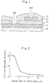
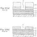
- a lower electrode 2 is formed out of a platinum film on a semiconductor substrate 1 .
- a capacitive insulating film 3 is formed out of a ferroelectric or high-dielectric-constant film on the lower electrode 2
- an upper electrode 4 is formed out of a platinum film on the capacitive insulating film 3 .
- a passivation film 5 is deposited on the upper electrode 4 to cover the electrode 4 entirely.
- a resist mask 6 with an opening for forming a contact hole is formed on the passivation film 5 .
- the passivation film 5 is dry-etched using the resist mask 6 , thereby forming a contact hole 7 in the passivation film 5 so as to reach the upper electrode 4 .
- the opening area of the contact hole 7 is 15 ⁇ m 2 , for example.
- the resist mask 6 is removed using oxygen radicals, which have been generated by decomposing oxygen gas with microwaves.
- the upper electrode 4 is exposed inside the contact hole 7 .
- insulating metal oxides, included in the ferroelectric or high-dielectric-constant film as the capacitive insulating film 3 are unintentionally reduced to deteriorate the electrical characteristics of the capacitor.
- An object of this invention is providing a capacitor with improved electrical characteristics by preventing insulating metal oxides, included in a ferroelectric or high-dielectric-constant film, from being reduced during the process step of removing a resist mask.
- the present inventors found that even when a large quantity of hydrogen is released from a resist mask, insulating metal oxides, included in a ferroelectric or high-dielectric-constant film, are hardly reduced by that hydrogen if the opening area of a contact hole, formed in a passivation film, is small.
- the present inventors analyzed from various angles the reasons why the insulating metal oxides, included in the ferroelectric or high-dielectric-constant film, are reduced if the resist mask is removed by using oxygen radicals that have been generated by decomposing oxygen gas with microwaves.
- oxygen radicals that have been generated by decomposing oxygen gas with microwaves.
- the following mechanism Specifically, if oxygen gas is decomposed with microwaves, then the density of electrons, existing in the resulting oxygen plasma, is high. Thus, a large quantity of hydrogen is released from the resist mask. Then, that released hydrogen is activated by the catalytic action of platinum contained in the upper electrode. Consequently, that activated hydrogen diffuses into the ferroelectric or high-dielectric-constant film as the capacitive insulating film to reduce the insulating metal oxides contained in the ferroelectric or high-dielectric-constant film.
- the opening area of a contact hole, formed in an insulating film covering a capacitor is defined at a predetermined value or less.
- the quantity of hydrogen produced from the resist mask is cut down during the removal thereof, thereby preventing hydrogen from diffusing into the ferroelectric or high-dielectric-constant film as the capacitive insulating film and from reducing the insulating metal oxides contained therein.
- a first exemplary capacitor according to the present invention includes a lower electrode, a capacitive insulating film, an upper electrode and a passivation film that are formed in this order on a substrate.
- the capacitive insulating film is made of an insulating metal oxide, which is a ferroelectric or a dielectric with a high relative dielectric constant.
- At least one contact hole is formed in the passivation film to connect the lower electrode to an interconnect for the lower electrode or connect the upper electrode to an interconnect for the upper electrode.
- the opening area of the contact hole is equal to or smaller than 5 ⁇ m 2 .
- a second exemplary capacitor according to the present invention includes a lower electrode, a capacitive insulating film, an upper electrode and a passivation film that are formed in this order on a substrate.
- the capacitive insulating film is made of an insulating metal oxide, which is a ferroelectric or a dielectric with a high relative dielectric constant.
- First and second contact holes are formed in the passivation film to connect the lower electrode to an interconnect for the lower electrode and the upper electrode to an interconnect for the upper electrode, respectively.
- the opening area of each of the first and second contact holes is equal to or smaller than 5 ⁇ m 2 .
- the opening area of each contact hole is equal to or smaller than 5 ⁇ m 2 . Accordingly, hydrogen, which is released from the resist mask during the process step of removing the mask to form the contact hole, hardly reaches the capacitive insulating film. That is to say, the insulating metal oxides, included in the ferroelectric or high-dielectric-constant film, are hardly reduced, thus greatly increasing the dielectric breakdown voltage of the capacitive insulating film.
- a first exemplary method for fabricating a capacitor according to the present invention includes the steps of: forming a capacitor including a lower electrode, a capacitive insulating film, an upper electrode and a passivation film by using a resist mask; and removing the resist mask.
- the capacitive insulating film is made of an insulating metal oxide, which is a ferroelectric or a dielectric with a high relative dielectric constant.
- the step of removing the mask includes removing the resist mask using a resist mask remover.
- a second exemplary method for fabricating a capacitor according to the present invention includes the steps of: forming a capacitor including a lower electrode, a capacitive insulating film and an upper electrode by using a resist mask; and removing the resist mask with at least one of the lower and upper electrodes exposed.
- the capacitive insulating film is made of an insulating metal oxide, which is a ferroelectric or a dielectric with a high relative dielectric constant.
- the step of removing the mask includes removing the resist mask using a resist mask remover.
- the resist mask is removed using a resist mask remover, almost no hydrogen is produced from the resist mask.
- the resist mask remover is preferably a material containing at least one of: an organic solvent; hydrofluoric acid; sulfuric acid; hydrochloric acid; nitric acid; ammonium hydroxide; and deionized hot water.
- the resist mask can be removed without producing hydrogen from the resist mask.
- a third exemplary method for fabricating a capacitor according to the present invention includes the steps of: forming a capacitor including a lower electrode, a capacitive insulating film and an upper electrode by using a resist mask; and removing the resist mask.
- the capacitive insulating film is made of an insulating metal oxide, which is a ferroelectric or a dielectric with a high relative dielectric constant.
- the step of removing the mask includes removing the resist mask using oxygen radicals that have been generated by decomposing ozone gas.
- a fourth exemplary method for fabricating a capacitor according to the present invention includes the steps of: forming a capacitor including a lower electrode, a capacitive insulating film and an upper electrode by using a resist mask; and removing the resist mask.
- the capacitive insulating film is made of an insulating metal oxide, which is a ferroelectric or a dielectric with a high relative dielectric constant.
- the step of removing the mask includes removing the resist mask using oxygen radicals that have been generated by decomposing oxygen gas with a plasma. The plasma has been generated in an inductively- or capacitively-coupled plasma processor.
- the oxygen radicals are generated by decomposing oxygen gas with a plasma that has been generated in an inductively- or capacitively-coupled plasma processor, almost no charged particles are included in the oxygen radicals. Accordingly, if the resist mask is removed using these oxygen radicals, the quantity of hydrogen released from the resist mask decreases.
- a fifth exemplary method for fabricating a capacitor according to the present invention includes the steps of: forming a capacitor including a lower electrode, a capacitive insulating film and an upper electrode by using a resist mask; and removing the resist mask.
- the capacitive insulating film is made of an insulating metal oxide, which is a ferroelectric or a dielectric with a high relative dielectric constant.
- the step of removing the mask includes removing the resist mask using oxygen radicals.
- the oxygen radicals are generated by decomposing oxygen gas with a plasma, which has been generated in a plasma generating chamber, and then are introduced into a plasma processing chamber.
- the plasma generating chamber and the plasma processing chamber are both included, and separated from each other, in a down-flow plasma processor.
- oxygen radicals generated by decomposing oxygen gas with a plasma that has been generated in the plasma generating chamber, are introduced into the plasma processing chamber. Accordingly, only these oxygen radicals with a longer lifetime than that of charged particles are introduced into the plasma processing chamber, and almost no charged particles are included in the oxygen radicals. Thus, if the resist mask is removed using such oxygen radicals, the quantity of hydrogen released from the resist mask decreases.
- a capacitor includes lower electrode 11 , capacitive insulating film 12 and upper electrode 13 , which are formed in this order on a semiconductor substrate 10 out of a first platinum film, a ferroelectric or high-dielectric-constant film and a second platinum film, respectively.
- a passivation film 14 is deposited thereon to cover the capacitor.
- first and second contact holes 16A and 16B are formed to connect the upper electrode 13 to an interconnect for the upper electrode and the lower electrode 11 to an interconnect for the lower electrode, respectively.
- the opening area of each of the first and second contact holes 16A and 16B is defined at 5 ⁇ m 2 or less.
- Figure 2 illustrates a relationship between the opening area of a contact hole and the dielectric breakdown voltage of a capacitor. As shown in Figure 2 , if the opening area is 5 ⁇ m 2 or less, the dielectric breakdown voltage of the capacitor abruptly increases.
- the dielectric breakdown voltage of the capacitor abruptly increases when the opening area of the contact hole is defined at 5 ⁇ m 2 or less.
- the opening area of the resist mask is defined at as small as 5 ⁇ m 2 or less, then almost no hydrogen reaches the capacitive insulating film 12 , and the insulating metal oxides, included in the ferroelectric or high-dielectric-constant film, are hardly reduced.
- the dielectric breakdown voltage of the capacitor greatly increases.
- a lower electrode 11 is formed out of a first platinum film, for example, on a semiconductor substrate 10 .
- a capacitive insulating film 12 is formed out of a ferroelectric or high-dielectric-constant film on the lower electrode 11
- an upper electrode 13 is formed out of a second platinum film, for example, on the capacitive insulating film 12 .
- a passivation film 14 is deposited on the upper electrode 13 to cover the lower electrode 11 , capacitive insulating film 12 and upper electrode 13 entirely.
- a mask with openings for forming contact holes e.g., a resist mask 15
- the passivation film 14 is dry-etched using the resist mask 15 , thereby forming first and second contact holes 16A and 16B to connect the upper electrode 13 to an interconnect for the upper electrode and the lower electrode 11 to an interconnect for the lower electrode, respectively, in the passivation film 14 .
- the upper and lower electrodes 13 and 11 are exposed inside the first and second contact holes 16A and 16B , respectively.
- the resist mask 15 is removed using a resist mask remover made of an organic solvent.
- the resist mask 15 is removed using a resist mask remover of an organic solvent, almost no hydrogen is produced from the resist mask 15 during the removal of the resist mask 15 .
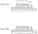
- a lower electrode 21 is formed out of a first platinum film, for example, on a semiconductor substrate 20 . Then, a ferroelectric or high-dielectric-constant film to be a capacitive insulating film 22 is formed on the lower electrode 21 , and a second platinum film to be an upper electrode 23 is deposited thereon. Next, a resist mask 24 is formed on the second platinum film.
- the second platinum film and ferroelectric or high-dielectric-constant film are etched in this order using the resist mask 24 , thereby forming the upper electrode 23 and capacitive insulating film 22 out of the second platinum film and ferroelectric or high-dielectric-constant film, respectively.
- the resist mask 24 is removed using a resist mask remover made of an organic solvent.
- the resist mask 24 is removed using a resist mask remover made of an organic solvent, almost no hydrogen is produced from the resist mask 24 during the process step of removing the resist mask 24 .
- a resist mask remover made of an organic solvent it is possible to prevent hydrogen from diffusing into the ferroelectric or high-dielectric-constant film as the capacitive insulating film and from reducing the insulating metal oxide included in the ferroelectric or high-dielectric-constant film.
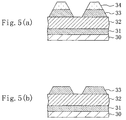
- a lower electrode 31 is formed out of a first platinum film, for example, on a semiconductor substrate 30 . Then, a ferroelectric or high-dielectric-constant film to be a capacitive insulating film 32 is formed on the lower electrode 31 , and a second platinum film to be an upper electrode 33 is deposited thereon. Next, a resist mask 34 is formed on the second platinum film.
- the second platinum film is etched using the resist mask 34 , thereby forming the upper electrode 33 out of the second platinum film.
- the resist mask 34 is removed using a resist mask remover made of an organic solvent.
- the resist mask 34 is removed using a resist mask remover made of an organic solvent, almost no hydrogen is produced from the resist mask 34 during the process step of removing the resist mask 34 .
- a resist mask remover made of an organic solvent it is possible to prevent hydrogen from diffusing into the ferroelectric or high-dielectric-constant film as the capacitive insulating film and from reducing the insulating metal oxide included in the ferroelectric or high-dielectric-constant film.
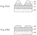
- a lower electrode 41 is formed out of a first platinum film, for example, on a semiconductor substrate 40 . Then, a ferroelectric or high-dielectric-constant film to be a capacitive insulating film 42 is deposited on the lower electrode 41 . Next, a resist mask 43 is formed on the ferroelectric or high-dielectric-constant film.
- the ferroelectric or high-dielectric-constant film is etched using the resist mask 43 , thereby forming the capacitive insulating film 42 .
- the resist mask 43 is removed using a resist mask remover made of an organic solvent.
- the resist mask 43 is removed using a resist mask remover made of an organic solvent, almost no hydrogen is produced from the resist mask 43 during the process step of removing the resist mask 43 .
- a lower electrode 51 is formed out of a first platinum film, for example, on a semiconductor substrate 50 . Then, a ferroelectric or high-dielectric-constant film to be a capacitive insulating film 52 is formed on the lower electrode 51 , and a silicon oxide film to be a passivation film 53 is deposited thereon. Next, a resist mask 54 is formed on the silicon oxide film.
- the silicon oxide film and the ferroelectric or high-dielectric-constant film are etched in this order using the resist mask 54 , thereby forming the passivation film 53 and the capacitive insulating film 52 , respectively.
- the resist mask 54 is removed using a resist mask remover made of an organic solvent.
- the resist mask 54 is removed using a resist mask remover made of an organic solvent, almost no hydrogen is produced from the resist mask 54 during the process step of removing the resist mask 54 .
- a resist mask remover made of an organic solvent it is possible to prevent hydrogen from diffusing into the ferroelectric or high-dielectric-constant film as the capacitive insulating film and from reducing the insulating metal oxide included in the ferroelectric or high-dielectric-constant film.
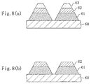
- a platinum film to be a lower electrode 61 and a ferroelectric or high-dielectric-constant film to be a capacitive insulating film 62 are deposited in this order on a semiconductor substrate 60 .
- a resist mask 63 is formed on the ferroelectric or high-dielectric-constant film.
- the ferroelectric or high-dielectric-constant film and the platinum film are etched in this order using the resist mask 63 , thereby forming the capacitive insulating film 62 and the lower electrode 61 .
- the resist mask 63 is removed using a resist mask remover made of an organic solvent.
- the resist mask 63 is removed using a resist mask remover made of an organic solvent, almost no hydrogen is produced from the resist mask 63 during the process step of removing the resist mask 63 .
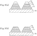
- platinum film to be a lower electrode 71 ferroelectric or high-dielectric-constant film to be a capacitive insulating film 72 and silicon oxide film to be a passivation film 73 are deposited in this order on a semiconductor substrate 70 .
- a resist mask 74 is formed on the silicon oxide film.
- the silicon oxide film, ferroelectric or high-dielectric-constant film and platinum film are etched in this order using the resist mask 74 , thereby forming the passivation film 73 , capacitive insulating film 72 and the lower electrode 71 , respectively.
- the resist mask 74 is removed using a resist mask remover made of an organic solvent.
- the resist mask 74 is removed using a resist mask remover made of an organic solvent, almost no hydrogen is produced from the resist mask 74 during the process step of removing the resist mask 74 .
- the resist mask is removed using a resist mask remover made of an organic solvent.
- the resist mask may be removed using a solvent containing at least one of: hydrofluoric acid; sulfuric acid; hydrochloric acid; nitric acid; ammonium hydroxide; and deionized hot water.
- the method of the ninth embodiment is different from the methods of the second through eighth embodiments only in the process step of removing the resist mask. Thus, only this mask removing process step will be described.
- ozone gas is decomposed by heating the ozone gas or by irradiating far infrared radiation to the ozone gas with or without heating the gas, thereby generating oxygen radicals without generating charged particles.
- the oxygen radicals generated are introduced onto the resist mask to cause a chemical reaction between the resist mask and the oxygen radicals and thereby decompose the resist mask into CO 2 and H 2 O.
- CO 2 and H 2 O are removed.
- the process of generating oxygen radicals by heating the ozone gas may be carried out under the conditions that the quantity of ozone introduced is 4.5 liters per minute and the temperature is 300°C, for example.
- oxygen radicals are generated by decomposing ozone gas, and therefore almost no charged particles exist in the resulting oxygen radicals.
- the resist mask is decomposed using such oxygen radicals, the quantity of hydrogen released from the resist mask decreases. Accordingly, it is possible to prevent hydrogen from diffusing into the ferroelectric or high-dielectric-constant film as the capacitive insulating film and from reducing the insulating metal oxide included in the ferroelectric or high-dielectric-constant film.
- the method of the tenth embodiment is also different from the methods of the second through eighth embodiments only in the process step of removing the resist mask. Thus, only this mask removing process step will be described.
- oxygen gas is introduced into the chamber of an inductively- or capacitively-coupled plasma processor, while at the same time a plasma is generated between counter electrodes or coaxial electrodes inside the chamber.
- the oxygen gas is decomposed with the plasma, thereby generating oxygen radicals.
- the oxygen radicals generated are introduced onto the semiconductor substrate placed on a stage within the chamber to cause a chemical reaction between the resist mask and the oxygen radicals and thereby decompose the resist mask into CO 2 and H 2 O. Finally, CO 2 and H 2 O are removed.
- This process is preferably carried out under the conditions that pressure inside the chamber is 0.5 Torr to 1 Torr, flow rate of the oxygen gas is 200 sccm to 500 sccm, radio frequency power applied to the counter or coaxial electrodes is 400 W to 1000 W at 13.56 MHz and temperature at the stage is 100°C to 200°C,
- the optimum processing conditions include: in-chamber pressure of 0.5 Torr; O 2 flow rate of 400 sccm; radio frequency power of 800 W at 13.56 MHz; and stage temperature of 150°C.
- oxygen radicals are generated by decomposing oxygen gas with a plasma that has been generated in an inductively- or capacitively-coupled plasma processor, and therefore almost no charged particles exist in the resulting oxygen radicals.
- the resist mask is decomposed using such oxygen radicals, the quantity of hydrogen released from the resist mask decreases. Accordingly, it is possible to prevent hydrogen from diffusing into the ferroelectric or high-dielectric-constant film as the capacitive insulating film and from reducing the insulating metal oxide included in the ferroelectric or high-dielectric-constant film.
- the method of the eleventh embodiment is also different from the methods of the second through eighth embodiments only in the process step of removing the resist mask. Thus, only this mask removing process step will be described.
- a down-flow plasma processor (also called a "downstream plasma processor") is used.
- a plasma generating chamber for generating oxygen radicals and a plasma processing chamber for resist removal are separately provided.
- oxygen gas is decomposed with a plasma generated in the plasma generating chamber, thereby generating oxygen radicals.
- only oxygen radicals with a longer lifetime than that of charged particles are introduced into the plasma processing chamber in accordance with a down-flow technique.
- the oxygen radicals introduced are supplied onto the semiconductor substrate placed on a stage within the chamber to cause a chemical reaction between the resist mask and the oxygen radicals.
- the resist mask is decomposed into CO 2 and H 2 O, which are ultimately removed.
- This process is preferably carried out under similar conditions to those adopted in the tenth embodiment, namely, pressure inside the chamber is 0.5 Torr to 1 Torr, flow rate of the oxygen gas is 200 sccm to 500 sccm, radio frequency power applied to the electrodes is 400 W to 1000 W at 13.56 MHz and temperature at the stage is 100°C to 200°C.
- the optimum processing conditions include: in-chamber pressure of 0.5 Torr; O 2 flow rate of 400 sccm; radio frequency power of 800 w at 13.56 MHz; and stage temperature of 150°C.
- oxygen radicals generated by decomposing oxygen gas with a plasma that has been generated in the plasma generating chamber, are introduced into the plasma processing chamber. That is to say, since only oxygen radicals with a longer lifetime than that of charged particles are introduced into the plasma processing chamber, almost no charged particles exist in the resulting oxygen radicals. Thus, if the resist mask is decomposed using such oxygen radicals, the quantity of hydrogen released from the resist mask decreases. Accordingly, it is possible to prevent hydrogen from diffusing into the ferroelectric or high-dielectric-constant film as the capacitive insulating film and from reducing the insulating metal oxide included in the ferroelectric or high-dielectric-constant film.
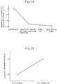
- Figure 10 illustrates respective contents of hydrogen (by an arbitrary unit) in a capacitive insulating film where a mask pattern is removed by a conventional method, with a resist mask remover (Embodiments 2 through 8), with oxygen radicals generated from ozone gas (Embodiment 9), with oxygen radicals generated in an inductively-coupled plasma processor (Embodiment 10) or with oxygen radicals generated in a down-flow plasma processor (Embodiment 11).
- the contents of hydrogen in the capacitive insulating film are much smaller than the content resulting from the conventional method.
- Figure 11 illustrates in comparison the dielectric breakdown voltages of respective capacitors formed by the conventional method and the methods of the present invention.
- the dielectric breakdown voltage of the capacitors formed by the methods of the present invention is 40 V, which is much higher than that of the capacitor formed by the conventional method (20 V).
Landscapes
- Semiconductor Integrated Circuits (AREA)
- Semiconductor Memories (AREA)
Abstract
Description
Claims (9)
- A capacitor comprising a lower electrode, a capacitive insulating film, an upper electrode and a passivation film that are formed in this order on a substrate, the capacitive insulating film being made of an insulating metal oxide, the metal oxide being a ferroelectric or a dielectric with a high relative dielectric constant,
wherein at least one contact hole is formed in the passivation film to connect the lower electrode to an interconnect for the lower electrode or connect the upper electrode to an interconnect for the upper electrode, and
wherein the opening area of the contact hole is equal to or smaller than 5µm2. - A capacitor comprising a lower electrode, a capacitive insulating film, an upper electrode and a passivation film that are formed in this order on a substrate, the capacitive insulating film being made of an insulating metal oxide, the metal oxide being a ferroelectric or a dielectric with a high relative dielectric constant,
wherein first and second contact holes are formed in the passivation film to connect the lower electrode to an interconnect for the lower electrode and the upper electrode to an interconnect for the upper electrode, respectively, and
wherein the opening area of each of the first and second contact holes is equal to or smaller than 5µm2. - A method for fabricating a capacitor, comprising the steps of:forming a capacitor including a lower electrode, a capacitive insulating film, an upper electrode and a passivation film by using a resist mask, the capacitive insulating film being made of an insulating metal oxide, the metal oxide being a ferroelectric or a dielectric with a high relative dielectric constant; andremoving the resist mask,
wherein the step of removing the mask includes removing the resist mask using a resist mask remover. - The method of Claim 3, wherein the resist mask remover is a material containing at least one of: an organic solvent; hydrofluoric acid; sulfuric acid; hydrochloric acid; nitric acid; ammonium hydroxide; and deionized hot water.
- A method for fabricating a capacitor, comprising the steps of:forming a capacitor including a lower electrode, a capacitive insulating film and an upper electrode by using a resist mask, the capacitive insulating film being made of an insulating metal oxide, the metal oxide being a ferroelectric or a dielectric with a high relative dielectric constant; andremoving the resist mask with at least one of the lower and upper electrodes exposed,
wherein the step of removing the mask includes removing the resist mask using a resist mask remover. - The method of Claim 5, wherein the resist mask remover is a material containing at least one of: an organic solvent; hydrofluoric acid; sulfuric acid; hydrochloric acid; nitric acid; ammonium hydroxide; and deionized hot water.
- A method for fabricating a capacitor, comprising the steps of:forming a capacitor including a lower electrode, a capacitive insulating film and an upper electrode by using a resist mask, the capacitive insulating film being made of an insulating metal oxide, the metal oxide being a ferroelectric or a dielectric with a high relative dielectric constant; andremoving the resist mask,
wherein the step of removing the mask includes removing the resist mask using oxygen radicals that have been generated by decomposing ozone gas. - A method for fabricating a capacitor, comprising the steps of:forming a capacitor including a lower electrode, a capacitive insulating film and an upper electrode by using a resist mask, the capacitive insulating film being made of an insulating metal oxide, the metal oxide being a ferroelectric or a dielectric with a high relative dielectric constant; andremoving the resist mask,
wherein the step of removing the mask includes removing the resist mask using oxygen radicals that have been generated by decomposing oxygen gas with a plasma, the plasma having been generated in an inductively-coupled plasma processor or a capacitively-coupled plasma processor. - A method for fabricating a capacitor, comprising the steps of:forming a capacitor including a lower electrode, a capacitive insulating film and an upper electrode by using a resist mask, the capacitive insulating film being made of an insulating metal oxide, the metal oxide being a ferroelectric or a dielectric with a high relative dielectric constant; andremoving the resist mask,
wherein the step of removing the mask includes removing the resist mask using oxygen radicals, the oxygen radicals being generated by decomposing oxygen gas with a plasma, which has been generated in a plasma generating chamber, and then introduced into a plasma processing chamber, the plasma generating chamber and the plasma processing chamber being both included, and separated from each other, in a down-flow plasma processor.
Applications Claiming Priority (2)
| Application Number | Priority Date | Filing Date | Title |
|---|---|---|---|
| JP14364298 | 1998-05-26 | ||
| JP14364298 | 1998-05-26 |
Publications (2)
| Publication Number | Publication Date |
|---|---|
| EP0961311A2 true EP0961311A2 (en) | 1999-12-01 |
| EP0961311A3 EP0961311A3 (en) | 2003-03-05 |
Family
ID=15343537
Family Applications (1)
| Application Number | Title | Priority Date | Filing Date |
|---|---|---|---|
| EP99110230A Withdrawn EP0961311A3 (en) | 1998-05-26 | 1999-05-26 | Capacitor and method for fabricating the same |
Country Status (5)
| Country | Link |
|---|---|
| US (1) | US20020182802A1 (en) |
| EP (1) | EP0961311A3 (en) |
| KR (1) | KR19990088548A (en) |
| CN (1) | CN1237792A (en) |
| TW (1) | TW460748B (en) |
Cited By (2)
| Publication number | Priority date | Publication date | Assignee | Title |
|---|---|---|---|---|
| US7026680B2 (en) | 2003-03-12 | 2006-04-11 | Fujitsu Limited | Thin film capacitive element, method for producing same and electronic device |
| US7161793B2 (en) | 2002-11-14 | 2007-01-09 | Fujitsu Limited | Layer capacitor element and production process as well as electronic device |
Families Citing this family (5)
| Publication number | Priority date | Publication date | Assignee | Title |
|---|---|---|---|---|
| JP2004095755A (en) * | 2002-08-30 | 2004-03-25 | Fujitsu Ltd | Method for manufacturing semiconductor device |
| JP4641396B2 (en) * | 2004-09-02 | 2011-03-02 | Okiセミコンダクタ株式会社 | Thin film capacitor and manufacturing method thereof |
| JP2006128309A (en) * | 2004-10-27 | 2006-05-18 | Shinko Electric Ind Co Ltd | Capacitor device and manufacturing method thereof |
| JP2008288281A (en) * | 2007-05-15 | 2008-11-27 | Hitachi Kokusai Electric Inc | Semiconductor device manufacturing method and substrate processing apparatus |
| CN102694091B (en) * | 2012-06-13 | 2015-06-17 | 佛山市国星光电股份有限公司 | Method for exposing electrodes in wafer level packaging and mask plate |
Family Cites Families (14)
| Publication number | Priority date | Publication date | Assignee | Title |
|---|---|---|---|---|
| US3787239A (en) * | 1970-09-25 | 1974-01-22 | Allied Chem | Chemical strippers and method of using |
| JPH0626201B2 (en) * | 1987-10-15 | 1994-04-06 | 富士通株式会社 | Method for manufacturing semiconductor device |
| US5719416A (en) * | 1991-12-13 | 1998-02-17 | Symetrix Corporation | Integrated circuit with layered superlattice material compound |
| US5822175A (en) * | 1995-04-13 | 1998-10-13 | Matsushita Electronics Corporation | Encapsulated capacitor structure having a dielectric interlayer |
| US5704986A (en) * | 1995-09-18 | 1998-01-06 | Taiwan Semiconductor Manufacturing Company Ltd | Semiconductor substrate dry cleaning method |
| JP3236220B2 (en) * | 1995-11-13 | 2001-12-10 | 東京応化工業株式会社 | Stripper composition for resist |
| JP2954877B2 (en) * | 1996-06-18 | 1999-09-27 | 松下電子工業株式会社 | Manufacturing method of capacitive element |
| JPH1022457A (en) * | 1996-07-03 | 1998-01-23 | Mitsubishi Electric Corp | Capacitance device, semiconductor device, and manufacturing method thereof |
| WO1998005071A1 (en) * | 1996-07-26 | 1998-02-05 | Symetrix Corporation | Method of fabricating an integrated circuit using self-patterned thin films |
| SG54548A1 (en) * | 1996-08-28 | 1998-11-16 | Texas Instruments Inc | Contact formation for a semiconductor device |
| TW396454B (en) * | 1997-06-24 | 2000-07-01 | Matsushita Electrics Corporati | Semiconductor device and method for fabricating the same |
| TW386289B (en) * | 1997-07-03 | 2000-04-01 | Matsushita Electronics Corp | Capacitance element and manufacturing thereof |
| US6642621B2 (en) * | 1997-12-24 | 2003-11-04 | Rohm Co., Ltd. | Capacitor-type semiconductor device |
| JP3276351B2 (en) * | 1999-12-13 | 2002-04-22 | 松下電器産業株式会社 | Method for manufacturing semiconductor device |
-
1999
- 1999-05-18 TW TW088108106A patent/TW460748B/en not_active IP Right Cessation
- 1999-05-25 CN CN99107551A patent/CN1237792A/en active Pending
- 1999-05-26 KR KR1019990018958A patent/KR19990088548A/en not_active Withdrawn
- 1999-05-26 EP EP99110230A patent/EP0961311A3/en not_active Withdrawn
-
2002
- 2002-07-15 US US10/194,323 patent/US20020182802A1/en not_active Abandoned
Cited By (3)
| Publication number | Priority date | Publication date | Assignee | Title |
|---|---|---|---|---|
| US7161793B2 (en) | 2002-11-14 | 2007-01-09 | Fujitsu Limited | Layer capacitor element and production process as well as electronic device |
| US7405921B2 (en) | 2002-11-14 | 2008-07-29 | Fujitsu Limited | Layer capacitor element and production process as well as electronic device |
| US7026680B2 (en) | 2003-03-12 | 2006-04-11 | Fujitsu Limited | Thin film capacitive element, method for producing same and electronic device |
Also Published As
| Publication number | Publication date |
|---|---|
| KR19990088548A (en) | 1999-12-27 |
| US20020182802A1 (en) | 2002-12-05 |
| TW460748B (en) | 2001-10-21 |
| EP0961311A3 (en) | 2003-03-05 |
| CN1237792A (en) | 1999-12-08 |
Similar Documents
| Publication | Publication Date | Title |
|---|---|---|
| US6368517B1 (en) | Method for preventing corrosion of a dielectric material | |
| US6211034B1 (en) | Metal patterning with adhesive hardmask layer | |
| US20010016226A1 (en) | Method for preparing the surface of a dielectric | |
| US6753133B2 (en) | Method and manufacturing a semiconductor device having a ruthenium or a ruthenium oxide | |
| US6458648B1 (en) | Method for in-situ removal of side walls in MOM capacitor formation | |
| US6645852B1 (en) | Process for fabricating a semiconductor device having recess portion | |
| US6746877B1 (en) | Encapsulation of ferroelectric capacitors | |
| EP0961311A2 (en) | Capacitor and method for fabricating the same | |
| EP1006582B1 (en) | Semiconductor memory device having a hydrogen barrier and method for manufacturing the same | |
| US20020058371A1 (en) | Method of manufacturing semiconductor device | |
| US6607963B2 (en) | Method for forming capacitor of semiconductor device | |
| US20030047532A1 (en) | Method of etching ferroelectric layers | |
| US7115518B2 (en) | Method for fabricating semiconductor device comprising forming holes in a multi-layer insulating film | |
| US6071787A (en) | Method of forming a capacitor including forming a first and second conductive layers and etching layers to form alloyed conductive sidewall spacers | |
| KR100517782B1 (en) | Method for producing a noble metal-containing structure on a substrate, and semiconductor component having such a noble metal-containing structure | |
| US7037848B2 (en) | Methods of etching insulative materials, of forming electrical devices, and of forming capacitors | |
| US6329237B1 (en) | Method of manufacturing a capacitor in a semiconductor device using a high dielectric tantalum oxide or barium strontium titanate material that is treated in an ozone plasma | |
| JPH1050951A (en) | Semiconductor device, and its manufacture | |
| US8076235B2 (en) | Semiconductor device and fabrication method thereof | |
| JP2000049311A (en) | Capacitive device and manufacture thereof | |
| US6713363B1 (en) | Method for fabricating capacitor of semiconductor device | |
| JP2000228499A (en) | Semiconductor memory and fabrication thereof | |
| JPH1131682A (en) | Dry etching method and manufacture of ferroelectric memory element | |
| JP2007067336A (en) | Semiconductor device manufacturing method and semiconductor device | |
| JPH1065117A (en) | Pattern formation method |
Legal Events
| Date | Code | Title | Description |
|---|---|---|---|
| PUAI | Public reference made under article 153(3) epc to a published international application that has entered the european phase |
Free format text: ORIGINAL CODE: 0009012 |
|
| AK | Designated contracting states |
Kind code of ref document: A2 Designated state(s): AT BE CH CY DE DK ES FI FR GB GR IE IT LI LU MC NL PT SE |
|
| AX | Request for extension of the european patent |
Free format text: AL;LT;LV;MK;RO;SI |
|
| RAP1 | Party data changed (applicant data changed or rights of an application transferred) |
Owner name: MATSUSHITA ELECTRIC INDUSTRIAL CO., LTD. |
|
| PUAL | Search report despatched |
Free format text: ORIGINAL CODE: 0009013 |
|
| AK | Designated contracting states |
Kind code of ref document: A3 Designated state(s): AT BE CH CY DE DK ES FI FR GB GR IE IT LI LU MC NL PT SE Designated state(s): AT BE CH CY DE DK ES FI FR GB GR IE IT LI LU MC NL PT SE |
|
| AX | Request for extension of the european patent |
Extension state: AL LT LV MK RO SI |
|
| STAA | Information on the status of an ep patent application or granted ep patent |
Free format text: STATUS: THE APPLICATION HAS BEEN WITHDRAWN |
|
| 17P | Request for examination filed |
Effective date: 20030827 |
|
| 18W | Application withdrawn |
Effective date: 20030926 |