EP0954768B1 - Method and apparatus for wafer-focusing - Google Patents
Method and apparatus for wafer-focusing Download PDFInfo
- Publication number
- EP0954768B1 EP0954768B1 EP97947339A EP97947339A EP0954768B1 EP 0954768 B1 EP0954768 B1 EP 0954768B1 EP 97947339 A EP97947339 A EP 97947339A EP 97947339 A EP97947339 A EP 97947339A EP 0954768 B1 EP0954768 B1 EP 0954768B1
- Authority
- EP
- European Patent Office
- Prior art keywords
- data
- height
- area
- calculating
- periodic
- Prior art date
- Legal status (The legal status is an assumption and is not a legal conclusion. Google has not performed a legal analysis and makes no representation as to the accuracy of the status listed.)
- Expired - Lifetime
Links
Images


Classifications
-
- G—PHYSICS
- G03—PHOTOGRAPHY; CINEMATOGRAPHY; ANALOGOUS TECHNIQUES USING WAVES OTHER THAN OPTICAL WAVES; ELECTROGRAPHY; HOLOGRAPHY
- G03F—PHOTOMECHANICAL PRODUCTION OF TEXTURED OR PATTERNED SURFACES, e.g. FOR PRINTING, FOR PROCESSING OF SEMICONDUCTOR DEVICES; MATERIALS THEREFOR; ORIGINALS THEREFOR; APPARATUS SPECIALLY ADAPTED THEREFOR
- G03F9/00—Registration or positioning of originals, masks, frames, photographic sheets or textured or patterned surfaces, e.g. automatically
- G03F9/70—Registration or positioning of originals, masks, frames, photographic sheets or textured or patterned surfaces, e.g. automatically for microlithography
- G03F9/7003—Alignment type or strategy, e.g. leveling, global alignment
- G03F9/7023—Aligning or positioning in direction perpendicular to substrate surface
- G03F9/7026—Focusing
Definitions
- the present invention relates to methods and apparatus for focusing in lithographic systems and more particularly to a method and apparatus for correcting focus errors due to variations in material properties over an area of subject material to be processed.
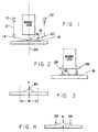
- Fig. 1 shows a central focus system wherein a light source 10 projects a ray 12, which is reflected by a mirror 14 to a point 16 on a surface 18.
- the ray 12 is reflected off of the surface 18, and by mirror 20 to a detector 22.
- a change in position of the surface 18 along the optical axis 24 results in a change of the reflected ray, and by various means this is used to detect the surface 18 position.
- the light may not reflect specularly from the top of the physical surface.
- the reflected beam is then no longer indicative of the surface 18 position and causes focus errors. Multiple rays can be used to sample multiple points on a wafer.
- position gauges include apparatus wherein the measurement is based on capacitance or air pressure. These devices must be remotely positioned from the central focusing area, and are known as non-central focusing systems. Such a system is indicated in Fig. 2, showing two position gauges 26 and 28. In a case where the gauges are of the capacitive type, the system has the disadvantage that variations in the composition of the material underlying surface 18 will affect the capacitance and cause faulty focusing.
- Figs. 3 and 4 illustrate a possible error "e” that can occur when a single point 30 is used, as in a central focusing system where an area of width w is being processed. For example, such an error could occur in a step and repeat process, where at a particular step the measurement point 30 differs in position along the optical axis by "e" from other points in the area.
- Fig. 4 illustrates a similar situation wherein an error "e” can occur when two focus gauges are used, taking measurements at points 32 and 34.
- Figs. 3 and 4 are particularly relevant in step and repeat systems, where at each step a particular area is illuminated in its entirety.
- a system is illustrated in Fig. 5a showing a wafer 33 illuminated over an area 34 through use of a lens 36 and reticle 37.
- the surface of the wafer 33 is illustrated in Fig. 5b, showing a number of the areas 34.
- Fig 6a For very large scale integrated circuits (VLSI), an alternate system known as "step and scan” is currently preferred, and illustrated in Fig 6a.
- the system illuminates only part of the areas 34 at any one time, and an entire area 34 is exposed by scanning the wafer 33 and reticle 38.
- the surface of the wafer is shown in Fig. 6b, wherein the smaller darkened area 39 indicates the illuminated portion of an area 34 at the start of a scan, and the attached arrow indicates the scan of the illumination across the area 34, which proceeds until the entire area has been illuminated.
- the system illuminates one of the areas, it moves the next area 34 to the optimum focal point and repeats the illumination process by scanning the area 34.
- the advantage of such a system is that the optics can be tuned more precisely over a smaller, narrower part 39 of the lens than for a larger area 34, reducing the difficulty in fabricating the optics to a high degree of quality. In spite of the improved optics of step and scan methods, the same type of focus errors discussed above occur.
- a preferred embodiment of the present invention includes a method and apparatus wherein the height over the complete surface of interest on a wafer/material is scanned and mapped, using either a central or non-central focus system.
- the type of data gathered is similar to that which is normally acquired in operation of the particular focusing system indicative of the wafer/material surface height. The difference is that according to the present invention, a much larger number of data points are sampled and then processed in a novel manner to provide improved focus information.
- These data are stored and used to calculate corrections in both the vertical position/height and tilt of the material/wafer for each exposure field, such as the areas (34) in Figs. 5b and 6b.
- the invention sorts out selected height data indicating periodic variations in surface height.
- Such data are normally not indicative of true wafer surface height variations, but instead are the result of periodic variations in wafer material composition caused by underlying structure relating to the particular circuitry. These periodic variations are distinguished from non-periodic variations, and are subtracted out of the total height measurement data to yield corrected surface height data.
- the present invention uses the corrected surface height data to calculate an optimum focus height for a given exposure area such as 34.
- An advantage of the present invention is that it improves focusing accuracy in step and scan systems.
- a further advantage of the present invention is that it improves focusing accuracy in step and repeat systems.
- a still further advantage of the present invention is that it provides corrections for focusing errors caused by periodic subject material composition variations.
- Another advantage of the present invention is that it optimizes focus in an illuminated wafer area containing real surface height irregularities.
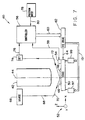
- a block diagram of the preferred embodiment of the present invention is shown as applied to a lithographic system 40.
- a projection lens system 42 having an optical axis 44 for projecting a pattern on a surface 46 of material 48, such as a wafer, secured to a positionable stage 50.
- the x, y and z coordinates are as indicated at 52, the z axis in alignment with the optics axis.
- the x,y position of stage 50 is detected by detection apparatus 54 and transmitted to controller 56 through bus 58.
- the controller 56 responds to program input 78 and sends stage drive signals through bus 60 to xyz drive 62, which acts upon the stage 50, indicated by line 64, to control the x, y and z position of the stage 50.
- the height of a particular point on the surface 46 of material 48 along the optic axis 44 is detected by a focusing system, which can be either the central or non-central type.
- a focusing system which can be either the central or non-central type.
- the system shown is of the central, optics type, and includes a light source 66 for emitting a ray 68, which is reflected by mirror 70 to the surface 46.
- the ray 68 is then reflected from surface 46 to mirror 72, which in turn reflects the ray to detector 74.
- a position indicating signal is then sent by detector 74 via line 76 to the controller 56.
- program input block 78 and input line 80 represent any type of programming of the controller 56 for directing the xyz drive 62 to scan the surface 46.
- the controller 56 collects and stores corresponding uncorrected surface height data provided by the detector 74.
- the controller 56 analyzes the stored data for periodic height variations occurring across the surface 46, and calculates corresponding periodic height variation data.
- the controller subtracts the periodic height variation data from the uncorrected height data to obtain corrected height data. This corrected height data is then used to calculate the optimum focus height i.e. position/height of the material for optimum focus over a specified area of the surface 46.
- the controller 56 is programmed to perform operations based on the corrected height data for a given area being illuminated. For example, referring to Fig. 5b, the controller 56 would be programmed for a step and repeat operation wherein an entire area 34 is illuminated in a single exposure. In such a case, the controller is programmed to calculate a focus height based on all of the height data points from the particular area 34. This could, for example, be the "average" height, or a height according to some other formula. In the step and scan operation illustrated in Fig. 6b, the controller would be similarly programmed to calculate a focus height based on the data collected for each smaller area 39. It is apparent that the step and scan procedure of Fig.
- the height data acquired and stored from the scanning operation discussed above is actually relative height data.
- a constant is applied to the data. This constant is usually determined empirically during equipment calibration, a procedure well understood by those skilled in the art.
- the above method can be used with any of the various focus systems, central on non-central, etc., and can be used with any method of moving the wafer/material surface relative to the optics axis, such as step and scan, step and repeat, etc.
- step and repeat systems the focus errors due to substrate composition would normally repeat at every area 34, since the underlying circuitry, etc. would be the same for each area being illuminated. Because of this, fixed focus offsets can be used for compensation.
- a pattern is shown representing height data obtained from scanning the surface of a wafer.
- the degree of darkness is indicative of the surface height.
- These variations correspond to variations in material 48 properties due to underlying circuitry, etc and are not indicative of true wafer surface height variations. Such variations cause erroneous focusing if correction for them is not made.
- Real height variations are generally random in nature, and show no particular pattern. For example, note the variations around the wafer edges, such as at 86.
- the present invention separates out the periodic data, normally indicative of artificial, non-real variations in surface height from data indicative of real variations that require a shift in the surface 46 height for optimum focus.
- f(x,y) represents the raw, uncorrected material surface height data, where x and y represent a position on the material surface 46.
- L x and L y are the distances in the x and y direction between periodic variations, and generally correspond to the areas 34 in Figs 5b and 6b, and are therefore quantities known to the user of the lithographic equipment.
- the controller 56 calculates f p (x,y) from the measured height data f(x,y) and subtracts it from the measured data f(x,y) to obtain the corrected height data f c (x,y).
- f p f p (x,y) from the measured height data f(x,y)
- f c f c
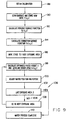
- Block 88 indicates the start up of the calibration routine.
- a wafer/material 48 has already been loaded onto the stage 50, and the programmed x and y step and scan data has been loaded into the controller 56 from program input 78.
- the controller is programmed for and scans the surface 46 and stores the raw height data f(x,y) for each programmed x, y position on surface 46 in a memory (not shown) in controller 56.
- the controller 56 then calculates the periodic height variation f p (x,y) from the uncorrected height data f(x,y) as indicated in block 92.
- the controller 56 then calculates the corrected height data f c (x,y), indicated in block 94.
- the controller then directs the stage to move the wafer to the first exposure area (block 96).
- the controller uses the corrected height data f c (x,y) for the various data points in the first exposure area to calculate an optimized focus height (block 98).
- this can be done in any of a number of ways.
- a preferred embodiment is to calculate the average height, and adjust according to the system constant which is normally empirically determined, as discussed above.
- the controller can determine if the area is as level as possible, i.e. perpendicular to the z axis, and calculate level adjustment data which can be applied to level adjusters, indicated as 97 and 99 in Fig. 7, and directed by the controller through line 60 in the xyz drive 62 and through bus 101.
- Controller 56 then adjusts the wafer height and directs the system to expose the wafer (block 100). Controller 56 then evaluates the x, y coordinates to determine if all the areas have been exposed (block 102). If not (104), stage 50 is moved to the next exposure area (block 106), and the process of blocks 98-102 is repeated, until the last area is exposed (108), whereupon the wafer process is complete (block 110).
- the method and apparatus of the present invention has particular industrial applicability in the area of photolithography. Within this area, applications in semiconductor fabrications and manufacturing of magnetic thin film heads are of particular interest.
- the present invention makes possible the construction of smaller etched line widths and gaps, due to the improved focusing provided. Smaller line widths and gaps translate to higher frequency, faster performance and smaller sized devices.
Description
- The present invention relates to methods and apparatus for focusing in lithographic systems and more particularly to a method and apparatus for correcting focus errors due to variations in material properties over an area of subject material to be processed.
- A variety of devices and methods have been used to determine the position of a surface along an optical axis for focusing, for example in lithographic systems and systems for measuring wafer flatness. Generally, they fall into one of two categories noted as either central or non-central focus systems. Fig. 1 shows a central focus system wherein a
light source 10 projects aray 12, which is reflected by amirror 14 to apoint 16 on asurface 18. Theray 12 is reflected off of thesurface 18, and bymirror 20 to adetector 22. A change in position of thesurface 18 along theoptical axis 24 results in a change of the reflected ray, and by various means this is used to detect thesurface 18 position. Because of inhomogeneity in the composition of the substrate, often due to circuit features, the light may not reflect specularly from the top of the physical surface. The reflected beam is then no longer indicative of thesurface 18 position and causes focus errors. Multiple rays can be used to sample multiple points on a wafer. - Other types of position gauges include apparatus wherein the measurement is based on capacitance or air pressure. These devices must be remotely positioned from the central focusing area, and are known as non-central focusing systems. Such a system is indicated in Fig. 2, showing two
position gauges material underlying surface 18 will affect the capacitance and cause faulty focusing. - In addition to errors introduced from material composition variations, either central or non-central systems can give erroneous focus indications due to the limited number of points that are sampled on the
surface 18. The focusing system for a lithography system should minimize the largest focus error within each exposure field. This problem is illustrated in Figs. 3 and 4. Fig. 3 illustrates a possible error "e" that can occur when asingle point 30 is used, as in a central focusing system where an area of width w is being processed. For example, such an error could occur in a step and repeat process, where at a particular step themeasurement point 30 differs in position along the optical axis by "e" from other points in the area. Fig. 4 illustrates a similar situation wherein an error "e" can occur when two focus gauges are used, taking measurements atpoints - The errors indicated in Figs. 3 and 4 that can occur due to the use of a limited number of measurement points, are particularly relevant in step and repeat systems, where at each step a particular area is illuminated in its entirety. Such a system is illustrated in Fig. 5a showing a
wafer 33 illuminated over anarea 34 through use of alens 36 andreticle 37. The surface of thewafer 33 is illustrated in Fig. 5b, showing a number of theareas 34. - For very large scale integrated circuits (VLSI), an alternate system known as "step and scan" is currently preferred, and illustrated in Fig 6a. The system illuminates only part of the
areas 34 at any one time, and anentire area 34 is exposed by scanning thewafer 33 andreticle 38. The surface of the wafer is shown in Fig. 6b, wherein the smaller darkenedarea 39 indicates the illuminated portion of anarea 34 at the start of a scan, and the attached arrow indicates the scan of the illumination across thearea 34, which proceeds until the entire area has been illuminated. After the system illuminates one of the areas, it moves thenext area 34 to the optimum focal point and repeats the illumination process by scanning thearea 34. The advantage of such a system is that the optics can be tuned more precisely over a smaller,narrower part 39 of the lens than for alarger area 34, reducing the difficulty in fabricating the optics to a high degree of quality. In spite of the improved optics of step and scan methods, the same type of focus errors discussed above occur. - From the above discussion, it is therefore apparent that an improved focus system is needed to reduce the errors caused by variations in material composition and errors that occur due to the use of limited numbers of data points.
- Briefly, a preferred embodiment of the present invention includes a method and apparatus wherein the height over the complete surface of interest on a wafer/material is scanned and mapped, using either a central or non-central focus system. The type of data gathered is similar to that which is normally acquired in operation of the particular focusing system indicative of the wafer/material surface height. The difference is that according to the present invention, a much larger number of data points are sampled and then processed in a novel manner to provide improved focus information. These data are stored and used to calculate corrections in both the vertical position/height and tilt of the material/wafer for each exposure field, such as the areas (34) in Figs. 5b and 6b. The invention sorts out selected height data indicating periodic variations in surface height. Such data are normally not indicative of true wafer surface height variations, but instead are the result of periodic variations in wafer material composition caused by underlying structure relating to the particular circuitry. These periodic variations are distinguished from non-periodic variations, and are subtracted out of the total height measurement data to yield corrected surface height data. The present invention uses the corrected surface height data to calculate an optimum focus height for a given exposure area such as 34.
- An advantage of the present invention is that it improves focusing accuracy in step and scan systems.
- A further advantage of the present invention is that it improves focusing accuracy in step and repeat systems.
- A still further advantage of the present invention is that it provides corrections for focusing errors caused by periodic subject material composition variations.
- Another advantage of the present invention is that it optimizes focus in an illuminated wafer area containing real surface height irregularities.
-
- Fig. 1 illustrates a prior art central focusing system;
- Fig. 2 illustrates a prior art non-central focusing system;
- Fig. 3 shows an error "e" that can occur when using a central focusing system;
- Fig. 4 illustrates how an error can occur when using a non-central focusing system;
- Fig. 5 shows a layout of identical circuits processed on a wafer by a prior art step and repeat system;
- Fig. 6 shows how a prior art step and scan procedure processes narrow rectangles to improve space utilization and allow improved optics;
- Fig. 7 shows a lithographic system utilizing the present invention;
- Fig. 8 is a pattern indicative of wafer surface height data variations; and
- Fig. 9 is a flow chart describing how a preferred embodiment of the present invention functions in the lithographic system of Fig. 7.
-
- Referring now to Fig. 7 of the drawing, a block diagram of the preferred embodiment of the present invention is shown as applied to a
lithographic system 40. There is aprojection lens system 42 having anoptical axis 44 for projecting a pattern on asurface 46 ofmaterial 48, such as a wafer, secured to apositionable stage 50. The x, y and z coordinates are as indicated at 52, the z axis in alignment with the optics axis. The x,y position ofstage 50 is detected bydetection apparatus 54 and transmitted tocontroller 56 throughbus 58. Thecontroller 56 responds toprogram input 78 and sends stage drive signals throughbus 60 toxyz drive 62, which acts upon thestage 50, indicated byline 64, to control the x, y and z position of thestage 50. - The height of a particular point on the
surface 46 ofmaterial 48 along theoptic axis 44 is detected by a focusing system, which can be either the central or non-central type. For illustrative purposes, the system shown is of the central, optics type, and includes alight source 66 for emitting aray 68, which is reflected bymirror 70 to thesurface 46. Theray 68 is then reflected fromsurface 46 to mirror 72, which in turn reflects the ray todetector 74. A position indicating signal is then sent bydetector 74 vialine 76 to thecontroller 56. - According to the present invention for the purpose of gathering
material 48surface 46 height data,program input block 78 andinput line 80 represent any type of programming of thecontroller 56 for directing the xyz drive 62 to scan thesurface 46. As thestage 50 moves thematerial 48 back and forth across theoptics axis 44, thecontroller 56 collects and stores corresponding uncorrected surface height data provided by thedetector 74. Thecontroller 56 then analyzes the stored data for periodic height variations occurring across thesurface 46, and calculates corresponding periodic height variation data. The controller then subtracts the periodic height variation data from the uncorrected height data to obtain corrected height data. This corrected height data is then used to calculate the optimum focus height i.e. position/height of the material for optimum focus over a specified area of thesurface 46. - In order to calculate the optimum focus height, the
controller 56 is programmed to perform operations based on the corrected height data for a given area being illuminated. For example, referring to Fig. 5b, thecontroller 56 would be programmed for a step and repeat operation wherein anentire area 34 is illuminated in a single exposure. In such a case, the controller is programmed to calculate a focus height based on all of the height data points from theparticular area 34. This could, for example, be the "average" height, or a height according to some other formula. In the step and scan operation illustrated in Fig. 6b, the controller would be similarly programmed to calculate a focus height based on the data collected for eachsmaller area 39. It is apparent that the step and scan procedure of Fig. 6b has an advantage over the step and repeat procedure of Fig. 6a in addition to the improved optics as above discussed due to the smaller area. This additional advantage is that the controller calculates focus for asmaller area 39, which results in a more accurate focus since points outside aparticular area 39 are not relevant and should not be included in the focus calculation. The errors occurring due to limited data points in prior art systems, as discussed in relation to Figs. 3 and 4 are largely eliminated by the scanning procedure of the present invention, which collects large quantities of height data. The calculation done on this data results in the determination of an improved, optimum focus height for the material for each particular area being illuminated. - The height data acquired and stored from the scanning operation discussed above is actually relative height data. In order to arrive at actual optimum focus height data for adjusting the position of the stage, a constant is applied to the data. This constant is usually determined empirically during equipment calibration, a procedure well understood by those skilled in the art.
- The above method can be used with any of the various focus systems, central on non-central, etc., and can be used with any method of moving the wafer/material surface relative to the optics axis, such as step and scan, step and repeat, etc. For step and repeat systems the focus errors due to substrate composition would normally repeat at every
area 34, since the underlying circuitry, etc. would be the same for each area being illuminated. Because of this, fixed focus offsets can be used for compensation. - Referring now to Fig. 8, a pattern is shown representing height data obtained from scanning the surface of a wafer. The degree of darkness is indicative of the surface height. Note the dark
gray areas 82 and the lightergray areas 84. They show a periodicity of "d" in the x direction. These variations correspond to variations inmaterial 48 properties due to underlying circuitry, etc and are not indicative of true wafer surface height variations. Such variations cause erroneous focusing if correction for them is not made. Real height variations are generally random in nature, and show no particular pattern. For example, note the variations around the wafer edges, such as at 86. - As discussed above, the present invention separates out the periodic data, normally indicative of artificial, non-real variations in surface height from data indicative of real variations that require a shift in the
surface 46 height for optimum focus. The surface height corrected for periodic variations is expressed aswhere
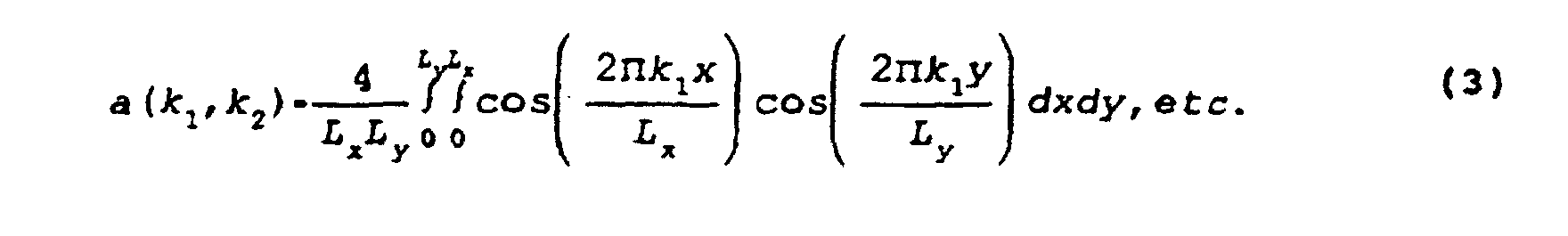
- f(x,y) represents the raw, uncorrected material surface height data, where x and y represent a position on the
material surface 46. Lx and Ly are the distances in the x and y direction between periodic variations, and generally correspond to theareas 34 in Figs 5b and 6b, and are therefore quantities known to the user of the lithographic equipment. k1 = π/Lx and k2 = π/Ly ao and a (k1 k2) ... d (k1 k2) are the Fourier coefficients. Thecontroller 56 calculates fp(x,y) from the measured height data f(x,y) and subtracts it from the measured data f(x,y) to obtain the corrected height data fc(x,y). Of course, as mentioned above, there is also a constant, non-varying height term (not shown). This is normally determined empirically by conventional methods. - Referring now to Fig. 9, a flow chart is shown illustrating a preferred embodiment of the processing performed by the
controller 56 according to the present invention, functioning cooperatively in thesystem 40.Block 88 indicates the start up of the calibration routine. At this point a wafer/material 48 has already been loaded onto thestage 50, and the programmed x and y step and scan data has been loaded into thecontroller 56 fromprogram input 78. This process is standard procedure and needs no further explanation for those skilled in the art. According to the present invention, inblock 90, the controller is programmed for and scans thesurface 46 and stores the raw height data f(x,y) for each programmed x, y position onsurface 46 in a memory (not shown) incontroller 56. Thecontroller 56 then calculates the periodic height variation fp(x,y) from the uncorrected height data f(x,y) as indicated inblock 92. Thecontroller 56 then calculates the corrected height data fc(x,y), indicated inblock 94. - The controller then directs the stage to move the wafer to the first exposure area (block 96). At this point, the controller uses the corrected height data fc (x,y) for the various data points in the first exposure area to calculate an optimized focus height (block 98). As mentioned above, this can be done in any of a number of ways. A preferred embodiment is to calculate the average height, and adjust according to the system constant which is normally empirically determined, as discussed above. In addition, the controller can determine if the area is as level as possible, i.e. perpendicular to the z axis, and calculate level adjustment data which can be applied to level adjusters, indicated as 97 and 99 in Fig. 7, and directed by the controller through
line 60 in thexyz drive 62 and throughbus 101. -
Controller 56 then adjusts the wafer height and directs the system to expose the wafer (block 100).Controller 56 then evaluates the x, y coordinates to determine if all the areas have been exposed (block 102). If not (104),stage 50 is moved to the next exposure area (block 106), and the process of blocks 98-102 is repeated, until the last area is exposed (108), whereupon the wafer process is complete (block 110). - The method and apparatus of the present invention has particular industrial applicability in the area of photolithography. Within this area, applications in semiconductor fabrications and manufacturing of magnetic thin film heads are of particular interest. The present invention makes possible the construction of smaller etched line widths and gaps, due to the improved focusing provided. Smaller line widths and gaps translate to higher frequency, faster performance and smaller sized devices.
- Although a preferred embodiment of the present invention has been described above, it will be appreciated that certain alterations and modifications thereof will become apparent to those skilled in the art. It is therefore intended that the appended claims be interpreted as covering all such alterations and modifications.
Claims (8)
- A method for improving focus on an area of a surface (46) of a material (48) to be processed in a lithographic system, said method comprising:(a) scanning said surface (46) to obtain uncorrected surface height data;(b) determining periodic height variation data from said uncorrected data;(c) subtracting said periodic height variation data from said uncorrected surface height data to create corrected surface height data;(d) calculating optimum focus height data from said corrected surface height data; and(e) setting the height of said surface to an optimum focus height corresponding to said optimum focus height data.
- A method as recited in claim 1 wherein said determining includes modeling said periodic height variation data with a Fourier series, and calculating a particular value of said periodic variation data from said Fourier series for use in said subtracting.
- A method as recited in claim 1 wherein said calculating includes calculating the average of said corrected surface height data as said optimum focus height data.
- A method as recited in claim 1 further comprising:(a) calculating surface level data of said surface from said corrected surface height data; and(b) adjusting said surface using said surface level data such that said area is optimally perpendicular to an optic axis of said lithographic system.
- An apparatus for improving focus on an area of a surface (46) of a material (48) to be processed in a lithographic system, said system having a projection lens system (42) having an optic axis (44), a stage (50) for positioning said material, means (74) for detecting the height of a point on said area of said surface, and means (62) for positioning said stage, said apparatus comprising:controller means (56) including(a) scanning means responsive to said means for detecting, for directing said means for positioning to scan said surface and obtain uncorrected surface height data;(b) means for determining periodic height variation data from said uncorrected data;(c) means for subtracting said periodic height variation data from said uncorrected surface height data to create corrected height data;(d) means for calculating optimum focus height data from said corrected surface height data; and(e) means for directing said means for positioning to position said stage so as to place said area at an optimum focus point along said optic axis.
- Apparatus as claimed in claim 5 wherein said means for determining includes means for modeling said periodic height variation data with a Fourier series, and calculating a particular value of said periodic variation data from said Fourier series for use in said subtracting.
- Apparatus as claimed in claim 5 wherein said means for calculating includes means for calculating the average of said corrected surface height data as said optimum focus height data.
- Apparatus as claimed in claim 5 wherein said controller means further includes(a) means for calculating surface level data of said surface from said corrected surface height data; and(b) means for directing said means for positioning to adjust said surface using said surface level data such that said area is optimally perpendicular to said optic axis.
Applications Claiming Priority (3)
| Application Number | Priority Date | Filing Date | Title |
|---|---|---|---|
| US08/788,124 US5748323A (en) | 1997-01-23 | 1997-01-23 | Method and apparatus for wafer-focusing |
| US788124 | 1997-01-23 | ||
| PCT/US1997/020034 WO1998033097A1 (en) | 1997-01-23 | 1997-11-04 | Method and apparatus for wafer-focusing |
Publications (2)
| Publication Number | Publication Date |
|---|---|
| EP0954768A1 EP0954768A1 (en) | 1999-11-10 |
| EP0954768B1 true EP0954768B1 (en) | 2005-04-20 |
Family
ID=25143509
Family Applications (1)
| Application Number | Title | Priority Date | Filing Date |
|---|---|---|---|
| EP97947339A Expired - Lifetime EP0954768B1 (en) | 1997-01-23 | 1997-11-04 | Method and apparatus for wafer-focusing |
Country Status (4)
| Country | Link |
|---|---|
| US (1) | US5748323A (en) |
| EP (1) | EP0954768B1 (en) |
| DE (1) | DE69733087T2 (en) |
| WO (1) | WO1998033097A1 (en) |
Cited By (2)
| Publication number | Priority date | Publication date | Assignee | Title |
|---|---|---|---|---|
| CN103676494A (en) * | 2012-09-25 | 2014-03-26 | 上海微电子装备有限公司 | Field-by-field focusing and leveling method for scanning lithography machine |
| DE102020124006B3 (en) | 2020-09-15 | 2022-01-05 | Laser Imaging Systems Gmbh | EXPOSURE CONTROL IN PHOTOLITHOGRAPHIC DIRECT EXPOSURE METHODS FOR CREATING CIRCUIT BOARDS OR CIRCUITS |
Families Citing this family (16)
| Publication number | Priority date | Publication date | Assignee | Title |
|---|---|---|---|---|
| US7116401B2 (en) * | 1999-03-08 | 2006-10-03 | Asml Netherlands B.V. | Lithographic projection apparatus using catoptrics in an optical sensor system, optical arrangement, method of measuring, and device manufacturing method |
| US6924884B2 (en) | 1999-03-08 | 2005-08-02 | Asml Netherlands B.V. | Off-axis leveling in lithographic projection apparatus |
| TW490596B (en) * | 1999-03-08 | 2002-06-11 | Asm Lithography Bv | Lithographic projection apparatus, method of manufacturing a device using the lithographic projection apparatus, device manufactured according to the method and method of calibrating the lithographic projection apparatus |
| GB2353649B (en) * | 1999-08-24 | 2003-10-29 | Analog Res And Dev Ltd | A method for improving focusing of an image to be projected onto a semiconductor wafer in a semiconductor manufacturing process |
| SG123601A1 (en) * | 2003-03-10 | 2006-07-26 | Asml Netherlands Bv | Focus spot monitoring in a lithographic projectionapparatus |
| EP1457828A3 (en) * | 2003-03-10 | 2009-04-22 | ASML Netherlands B.V. | Focus spot monitoring in a lithographic projection apparatus |
| US6975407B1 (en) * | 2004-05-19 | 2005-12-13 | Taiwan Semiconductor Manufacturing Co, Ltd. | Method of wafer height mapping |
| JP4843272B2 (en) * | 2004-07-31 | 2011-12-21 | カール・ツァイス・エスエムティー・ゲーエムベーハー | Optical system for microlithographic projection exposure apparatus |
| CN103545174B (en) * | 2012-07-16 | 2016-08-24 | 无锡华润上华科技有限公司 | Photoetching focusing parameter testing method and system |
| US10274838B2 (en) * | 2013-03-14 | 2019-04-30 | Taiwan Semiconductor Manufacturing Company, Ltd. | System and method for performing lithography process in semiconductor device fabrication |
| CN107735731B (en) * | 2015-07-03 | 2020-12-22 | Asml荷兰有限公司 | Lithographic apparatus, control method and computer program product |
| KR102037994B1 (en) * | 2015-07-20 | 2019-10-29 | 에이에스엠엘 네델란즈 비.브이. | Method of controlling lithographic apparatus, lithographic apparatus and device manufacturing method |
| CN108027572B (en) * | 2015-09-15 | 2020-09-18 | Asml荷兰有限公司 | Method for controlling a lithographic apparatus, lithographic apparatus and device manufacturing method |
| CN111352304B (en) * | 2018-12-24 | 2021-11-19 | 上海微电子装备(集团)股份有限公司 | Focusing and leveling device, photoetching equipment and focusing and leveling method |
| US11442021B2 (en) * | 2019-10-11 | 2022-09-13 | Kla Corporation | Broadband light interferometry for focal-map generation in photomask inspection |
| CN112904679B (en) * | 2021-01-26 | 2023-01-17 | 长鑫存储技术有限公司 | Method for determining focus boundary and judging whether wafer needs to be reworked |
Family Cites Families (5)
| Publication number | Priority date | Publication date | Assignee | Title |
|---|---|---|---|---|
| US3904290A (en) * | 1974-02-04 | 1975-09-09 | Xerox Corp | Optical system alignment apparatus |
| US4615621A (en) * | 1982-04-02 | 1986-10-07 | Eaton Corporation | Auto-focus alignment and measurement system and method |
| JPS58179834A (en) * | 1982-04-14 | 1983-10-21 | Canon Inc | Copying device and focus correcting method |
| JPS6147633A (en) * | 1984-08-13 | 1986-03-08 | Canon Inc | Projected exposure apparatus |
| JP3265504B2 (en) * | 1993-10-12 | 2002-03-11 | 株式会社ニコン | Exposure method and apparatus, and method for manufacturing semiconductor element |
-
1997
- 1997-01-23 US US08/788,124 patent/US5748323A/en not_active Expired - Lifetime
- 1997-11-04 WO PCT/US1997/020034 patent/WO1998033097A1/en active IP Right Grant
- 1997-11-04 DE DE69733087T patent/DE69733087T2/en not_active Expired - Lifetime
- 1997-11-04 EP EP97947339A patent/EP0954768B1/en not_active Expired - Lifetime
Cited By (4)
| Publication number | Priority date | Publication date | Assignee | Title |
|---|---|---|---|---|
| CN103676494A (en) * | 2012-09-25 | 2014-03-26 | 上海微电子装备有限公司 | Field-by-field focusing and leveling method for scanning lithography machine |
| CN103676494B (en) * | 2012-09-25 | 2015-11-18 | 上海微电子装备有限公司 | For the Field by field focusing and leveling method of scanning photoetching machine |
| DE102020124006B3 (en) | 2020-09-15 | 2022-01-05 | Laser Imaging Systems Gmbh | EXPOSURE CONTROL IN PHOTOLITHOGRAPHIC DIRECT EXPOSURE METHODS FOR CREATING CIRCUIT BOARDS OR CIRCUITS |
| WO2022057981A1 (en) | 2020-09-15 | 2022-03-24 | Laser Imaging Systems Gmbh | Exposure control in photolithographic direct exposure methods for manufacturing circuit boards or circuits |
Also Published As
| Publication number | Publication date |
|---|---|
| EP0954768A1 (en) | 1999-11-10 |
| WO1998033097A1 (en) | 1998-07-30 |
| DE69733087T2 (en) | 2006-03-02 |
| US5748323A (en) | 1998-05-05 |
| DE69733087D1 (en) | 2005-05-25 |
Similar Documents
| Publication | Publication Date | Title |
|---|---|---|
| EP0954768B1 (en) | Method and apparatus for wafer-focusing | |
| US6360012B1 (en) | In situ projection optic metrology method and apparatus | |
| US7081948B2 (en) | System for automated focus measuring of a lithography tool | |
| US20040223157A1 (en) | Position measuring device, position measurement method, exposure apparatus, exposure method, and superposition measuring device and superposition measurement method | |
| US10488180B2 (en) | Mask inspection apparatus and mask inspection method | |
| EP0919803A1 (en) | Method and compact system for inspecting a reticle with high accuracy | |
| US6721047B2 (en) | Method and apparatus for inspecting defects of a specimen | |
| US6416912B1 (en) | Method of manufacturing microdevice utilizing combined alignment mark | |
| US20020001403A1 (en) | Focusing control mechanism, and inspection apparatus using same | |
| CN107924852A (en) | Technology and system for the critical dimension measurement based on model | |
| KR20130073886A (en) | Inspecting apparatus and inspecting method | |
| US5973773A (en) | Lens distortion measurement using moire fringes | |
| JP2003066341A (en) | Reticle inspection device | |
| US20060192931A1 (en) | Automated focus feedback for optical lithography tool | |
| US7248351B2 (en) | Optimizing light path uniformity in inspection systems | |
| JPH11214289A (en) | Position measurement method and exposure method using the same | |
| US20060194130A1 (en) | Run to run control for lens aberrations | |
| JP3466730B2 (en) | Pattern evaluation apparatus and pattern evaluation method | |
| US20060193532A1 (en) | Optimizing focal plane fitting functions for an image field on a substrate | |
| US20060192943A1 (en) | Optimizing focal plane fitting functions for an image field on a substrate | |
| US20060193531A1 (en) | System for analyzing images of blazed phase grating samples | |
| KR100601661B1 (en) | Method and apparatus for measuring linear spot or position variations in a scanning system | |
| US6337486B2 (en) | Electron beam drawing process and electron beam drawing apparatus | |
| US20080202201A1 (en) | Device and method for automatic detection of incorrect measurements by means of quality factors | |
| JP2010025575A (en) | Film thickness measurement method and apparatus |
Legal Events
| Date | Code | Title | Description |
|---|---|---|---|
| PUAI | Public reference made under article 153(3) epc to a published international application that has entered the european phase |
Free format text: ORIGINAL CODE: 0009012 |
|
| 17P | Request for examination filed |
Effective date: 19990329 |
|
| AK | Designated contracting states |
Kind code of ref document: A1 Designated state(s): DE FR GB NL |
|
| GRAP | Despatch of communication of intention to grant a patent |
Free format text: ORIGINAL CODE: EPIDOSNIGR1 |
|
| GRAS | Grant fee paid |
Free format text: ORIGINAL CODE: EPIDOSNIGR3 |
|
| GRAA | (expected) grant |
Free format text: ORIGINAL CODE: 0009210 |
|
| AK | Designated contracting states |
Kind code of ref document: B1 Designated state(s): DE FR GB NL |
|
| PG25 | Lapsed in a contracting state [announced via postgrant information from national office to epo] |
Ref country code: NL Free format text: LAPSE BECAUSE OF FAILURE TO SUBMIT A TRANSLATION OF THE DESCRIPTION OR TO PAY THE FEE WITHIN THE PRESCRIBED TIME-LIMIT Effective date: 20050420 |
|
| REG | Reference to a national code |
Ref country code: GB Ref legal event code: FG4D |
|
| REF | Corresponds to: |
Ref document number: 69733087 Country of ref document: DE Date of ref document: 20050525 Kind code of ref document: P |
|
| NLV1 | Nl: lapsed or annulled due to failure to fulfill the requirements of art. 29p and 29m of the patents act | ||
| PLBE | No opposition filed within time limit |
Free format text: ORIGINAL CODE: 0009261 |
|
| STAA | Information on the status of an ep patent application or granted ep patent |
Free format text: STATUS: NO OPPOSITION FILED WITHIN TIME LIMIT |
|
| ET | Fr: translation filed | ||
| 26N | No opposition filed |
Effective date: 20060123 |
|
| REG | Reference to a national code |
Ref country code: GB Ref legal event code: 732E Free format text: REGISTERED BETWEEN 20091210 AND 20091216 |
|
| REG | Reference to a national code |
Ref country code: FR Ref legal event code: TP |
|
| PGFP | Annual fee paid to national office [announced via postgrant information from national office to epo] |
Ref country code: FR Payment date: 20101109 Year of fee payment: 14 |
|
| PGFP | Annual fee paid to national office [announced via postgrant information from national office to epo] |
Ref country code: DE Payment date: 20101130 Year of fee payment: 14 |
|
| PGFP | Annual fee paid to national office [announced via postgrant information from national office to epo] |
Ref country code: GB Payment date: 20101022 Year of fee payment: 14 |
|
| GBPC | Gb: european patent ceased through non-payment of renewal fee |
Effective date: 20111104 |
|
| REG | Reference to a national code |
Ref country code: FR Ref legal event code: ST Effective date: 20120731 |
|
| PG25 | Lapsed in a contracting state [announced via postgrant information from national office to epo] |
Ref country code: GB Free format text: LAPSE BECAUSE OF NON-PAYMENT OF DUE FEES Effective date: 20111104 |
|
| PG25 | Lapsed in a contracting state [announced via postgrant information from national office to epo] |
Ref country code: FR Free format text: LAPSE BECAUSE OF NON-PAYMENT OF DUE FEES Effective date: 20111130 |
|
| REG | Reference to a national code |
Ref country code: DE Ref legal event code: R119 Ref document number: 69733087 Country of ref document: DE Effective date: 20130601 |
|
| PG25 | Lapsed in a contracting state [announced via postgrant information from national office to epo] |
Ref country code: DE Free format text: LAPSE BECAUSE OF NON-PAYMENT OF DUE FEES Effective date: 20130601 |