FIELD OF THE INVENTION
-
This invention relates to micro yaw rate sensors suitable for measuring yaw rate
around its sensing axis. More particularly, to micro yaw rate sensors fabricated with Z cut
quartz wafer.
PRIOR ART AND BACKGROUND OF THE INVENTION
-
A micro yaw rate sensor, which is also called micro gyro, micro gyroscope or
micro vibrating angular rate sensor, is a micromachined resonator with resonance sensing
capability. The operation principle of the sensor follows. A linear momentum is created
by an alternate driving force which excites the resonator in an oscillation. This resonance
will be called driving resonance. Conservation of linear momentum implies that the
vibration is restricted to the driving resonance plane defined by driving force. However,
this plane is altered when the sensor is rotated around an axis parallel to the plane but
perpendicular to the movement of the resonator. The original vibration, which resists this
change, compensates this change by initiating a vibration out of the driving resonance
plane. The amplitude of this second vibration, which is induced by the so called Coriolis
force, is proportional to the speed of rotation in the direction perpendicular to both the
driving resonance plane and the axis of rotation. This secondary resonance, which will be
called the sensing resonance, can be detected by electric means and is indicative of
rotational speed, namely, the yaw rate.
-
Based on the above principles, various micro yaw rate sensors have been
invented, and their descriptions are available in patent and other technical literature. For
example, U. S. Patent (U.S.P.). Nos.5500549, 5635739, 5635639, 5515724, 5627314,
5331853, 5241861, 5505084, 5496436, 5408877, 5349855, 5331852, 5203208 and
5329815 describe various silicon based vibrational yaw rate sensors and their fabrication
and control methods; U. S. P. Nos. 5650568, 5226321, 5696323 and 5555765, disclose
vibrating wheel type yaw rate sensors; U. S. P. Nos. 5585562, 5166571, 5488863,
3839915, 4524619, 4898032 and 4538461 disclose various tuning fork type yaw rate
sensors; U. S. P. Nos. 5719335 and 5719335 disclose two types of electrostatically driven
rotational yaw rate sensors, and 5168756 discloses a type of electromagnetically driven
rotational yaw rate sensor, U. S. P. No 5656777, 5476007, 4791815 discloses various
miniature, but non micromachined vibrating yaw rate sensors and U. S. P. No. 5396797
describes yaw rate sensors formed by triaxial accelerometers.
-
Although many micro yaw rate sensors have been invented to date, none of them
has been developed into a successful mass produced commercial product yet. With a
review of the prior arts, it is apparent to those skilled in the art that most of the micro yaw
rate sensors invented so far, has one or more disadvantages associated therewith,
including: (a) sophisticated structure, (b) sophisticated frequency tuning and signal
processing circuits, (c) expansive packaging, (d) low long term stability and reliability
material, (e) high cost fabrication equipment, (f) high overall manufacturing cost.
-
Accordingly, there exists a need in many industries, especially in auto industry,
for new micro yaw rate sensors, having the following characteristics: (a) simple structure,
(b) simple driving/sensing circuitry, (c) easy to package, (d) high long term stability and
reliability, (e) easy to fabricate, (f) low manufacturing cost.
SUMMARY OF THE INVENTION
-
In general, the present invention provides a micro yaw rate sensor for measuring a
yaw rate about its sensing axis. The sensor comprises, at least, (a) a base made of a Z cut
quartz wafer; (b) a proof mass; (c) two sets of suspensions, namely, a first suspension and
a second suspension, supporting said proof mass from two sides and connecting said
proof mass to said base; (d) a plural number of driving electrodes patterned on said first
suspension; (e) a plural number of sensing electrodes patterned on said second
suspension. Said proof mass, said suspensions, and said electrodes together form an
electrically excitable resonator, fabricated from/on said base wafer by micromachining
technique. By impressing an alternating electric potential thereon said driving electrodes,
a driving resonance will be excited within the wafer plane. When a yaw motion around
the sensing axis occurs, a Coriolis force would force the resonator to resonant in the
direction perpendicular to the wafer plane. Electric measurement means connected to said
sensing electrodes detect electric charge signals induced by this sensing resonance which
is indicative of said yaw rate.
BRIEF DESCRIPTION OF THE DRAWINGS
-
- FIG. 1. is a schematic representation of a Y-beam of single crystal quartz, and its
piezoelectrically charged cross-sections under three loading cases.
- FIG. 2. is a schematic representation of a Y-beam of single crystal quartz with six
thin wire electrodes on top and bottom surfaces.
- FIG. 3 is a structural representation of a quartz yaw rate sensor, made in
accordance with the principles of the present invention.
- FIG. 4 is an exemplary electric circuit diagram used in a quartz yaw rate sensor,
made in accordance with the principles of the present invention.
- FIG. 5 is a schematic representation of a first embodiment of a quartz yaw rate
sensor, made in accordance with the principles of the present invention.
- FIG. 6 is a schematic representation of a second embodiment of a quartz yaw rate
sensor, made in accordance with the principles of the present invention.
-
PRINCIPLE OF THE INVENTION
-
The theory underlying the vibrating yaw rate sensor is well known, and will not
be discussed below. However, a short introduction has been given in the section entitled
"BACKGROUND OF THE INVENTION". According to the information obtained
through a review of the prior art, most micro yaw rate sensors fabricatable by regular
lithography techniques are build on silicon or metallic materials. These prior art micro
sensors commonly use either electrostatic or electromagnetic force to power the driving
resonance, and use capacitive measurement to detect the sensing resonance. The present
invention, however, provides a type of micro yaw rate sensor based on piezoelectric
effect in both the driving and sensing mechanisms. This differs from all silicon based
micro yaw rate sensors of the prior art. More specifically, the sensor of present invention
uses a resonator made of a monocrystalline Z cut quartz wafer. The simple structure of
the sensor results from unique designs of the driving and sensing electrodes, and it can
work with a simple signal processing circuit, and is highly suitable for low cost mass
production by micromachining.
-
It should be noticed here that, although the sensors of the present invention use
the same quartz wafer as some of the tuning fork type yaw rate sensors of the prior art,
there are several significant differences in design principle and in resonator structure
between the two. Detailed discussion on these differences will be given later in the
section entitled "DESCRIPTION OF PREFERRED EMBODIMENTS"
-
A simple introduction of monocrystalline quartz material follows (see ref). The
chemical composition of quartz is SiO2. The Si atoms are in four-coordination with
oxygen and constitute the (SiO4) tetrahedron, which is the basic unit of the structure. Each
oxygen is shared with two Si atoms. Quartz belongs to the trigonal trapezohedral class
(32) of the rhombohedral subsystem. The lattice type is hexagonal. This class is
characterized by one axis of three-fold symmetry and three polar axes of two-fold
symmetry perpendicular thereto and separated by angles of 120 degree. There is no center
of symmetry and no plane of symmetry. The axes of reference (X, Y, Z) are chosen such
that X is one of the axes of two-fold symmetry and Z is the axis of three-fold symmetry.
Apparently, cuffing a crystal at different planes will result in wafers with various different
properties. One of the most widely used wafers is that which is cut out of a quartz crystal
at the X-Y plane perpendicular to the Z axis, and is commonly called the Z cut wafer.
-
A property of quartz that has found an important application in the present
invention is piezoelectricity. The piezoelectric effect comes from an atomic dipole
structure of the quartz. The value of the polarizing effect of each dipole is proportional to
the local stress at the dipole. This dipole describes the local piezoelectric behavior of the
quartz at each atomic unit cell level well, but the global behavior is better described by
the resulting charge distribution. That is, the dipoles within the material can be fully or
partially neutralized by neighboring dipoles, while the dipoles at the boundaries cannot be
neutralized in the same way. The consequent charge distributions are shown in figure 1
where a rectangular cross-sectioned beam extending in the Y direction fabricated out of a
Z-cut quartz wafer, which is called a Y beam, is under three different loads.
-
Based on the above discussion, the piezoelectric charge build-up due to external
force on the Y beam can be read out through six simple thin wire electrodes shown in
figure 2. Alternatively, the electrodes can be used to impose an electric field on the quartz
to produce a piezoelectric force within the beam, equivalent of an external force. For
instance, short circuiting symmetrical electrodes in both sides, that is connecting
electrodes 1 to 4, 2 to 5 and 3 to 6, then grounding electrode 2 while imposing an electric
potential on electrodes 1 and 3 can create a bending force within the beam. The tip of the
beam, under this bending force, is bent over to the X direction. Apparently, this simple
cantilever beam, the Y quartz beam, can be used as a simple resonator by imposing an
alternating voltage on a proper pair (or pairs) of electrodes, and vice versa, it can be used
as a simple accelerometer by measuring the strain caused by inertial force with proper
pair (or pairs) electrodes. For instance, movement in the Z direction can be detected by
Vz=V1-V4 , while resonance in the X direction can be detected by 2Vx=(V2-V3)+(V4-V5),
where subscript x, y and z indicate the direction of the strain while the numerals indicate
the number of the sensing electrodes.
-
A simplified sensor structure of the present invention is a resonator
micromachined on a quartz wafer shown in figure 3. It has a proof mass and two
suspension beams. This simple resonator is symmetric in the x, the y, and the z direction
of quartz crystal. Three thin wire driving electrodes are double side patterned along the
edges and the centerlines of each beam. When an alternating voltage is applied to the
driving electrodes, it piezoelectrically excites a driving resonance within the wafer plane.
Now rotating the sensor around the Y axis, the Coriolis force would occur and will induce
a sensing resonance at the same frequency as the driving resonance but in the direction
perpendicular to the wafer plane. Since the Coriolis force increases proportionally with
the resonant speed of the proof mass, the out of plane movement of the proof mass
reaches its maximum value when the driving resonance reaches its maximum speed at its
neutral point. In other words, the movement of the proof mass which is a combined effect
of driving force and Coriolis force is an ellipse. The horizontal axis of the ellipse is in
proportion to the driving force while the vertical axis is in proportion to the yaw rate.
Using appropriate calculations, the effect of driving resonance and sensing resonance can
be separated. The piezoelectric signals corresponding to the sensing resonance induced by
Coriolis force are used to detect the yaw rate.
-
One exemplary circuit block diagram is shown in figure 4. Typical electric signals
flowing through the circuits are as follows. A driver module connected to the driving
electrodes generates a voltage wave Vd =V0 sin(ωt) at driving frequency ω to excite the
resonator into the driving resonance Xd=X0 sin(ωt), where 0 indicates a constant value of
the variables, subscript d indicates the variables related to the driving resonance while
subscript s indicates the variables related to the sensing resonance. Assuming the sensor
rotates at yaw rate Ω, a signal amplifier module connected to the sensing electrodes picks
up the piezoelectric charge signals induced by both driving and sensing resonance and
convert it to voltage output. In an ideal situation where no motion other than the yaw
motion exists, the converted voltage signals from the sensing electrodes are Vd= ksV0
sin(ωt), and Vs= kdΩ V0 cos(ωt), where ks and kd are coefficients of sensitivity.
Apparently, the Vs is a driving-frequency ω modulated signal, and its envelope, which
can be obtained through a demodulator, is in proportion to Ω, the yaw rate to be detected.
Subsequently, a demodulator module separating the modulated low frequency signal Ω
from high frequency modulating signal kd V0 cos(ωt) is all it needed to readout the yaw
rate. In reality, however, the yaw motion is often accompanied together with acceleration
in both the X direction (ax) and the Z direction (az). Since the acceleration would also
generate piezoelectric charge in sensing electrodes, the output from the amplifier module
in general become Vd=kd V0 sin(ωt)+ax , and Vs= ks Ω V0 cos(ωt)+az . In most practical
applications, such as automobile stability control, acceleration imposed on the sensor is at
a frequency far below that of the sensor resonance. Moreover, the portion of the signal
output related to the acceleration is not modulated by the resonance frequency. Therefore,
installing between the demodulator and amplifier modules a narrow band pass filter at
resonance frequency, which will eliminate any signals other than those resonant
frequency modulated signals, would prevent the unwanted acceleration from affecting the
sensor output in most cases.
-
In general, the sensitivity of the sensor to yaw rate to be detected increases with
(a) the Q factor of the sensing resonance, (b) the product of the amplitude and frequency
of the driving resonance. While the dynamics of the sensor response to a change in yaw
rate increases with the frequency of the resonance.
-
In summary, the present invention provides micro yaw rate sensors designed with
unique thin wire driving and sensing electrodes fabricated on top and bottom surfaces of a
Z cut monocrystalline quartz wafer, and it differs with all micro sensors of the prior art in
driving and sensing principles as well as in resonator structure. These sensors have the
following advantages: (a) a simple structure; (b) easy to fabricate with commonly
available micromachining equipment; (c) operatable at wide temperature range with good
temperature stability; (d) a linear response; (e) easy to process output signal; (f) easy to
package; (g) good long term stability; (h) easy to adjust sensitivity and dynamic range
with dimensional change of the proof mass. In summary, the sensor structure are suitable
for mass production with micro-machining equipment commonly available in the
semiconductor industry.
-
The above and other effects, features and advantages of the present invention will
be apparent to those skilled in the art from the following detailed description of various
embodiments thereof, in conjunction with the accompanying drawings.
DESCRIPTION OF PREFERRED EMBODIMENTS
-
The basic structure of a yaw rate sensor made in accordance with the principle of
the present invention comprises a base, a first suspension and a second suspension
mounted on the base, a proof mass supported by two suspensions in such a manner that
the first and second suspensions face each other across the proof mass. On the top and
bottom surfaces of the first suspension there are driving electrodes, and on the second
suspension there are sensing electrodes.
-
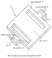
More specifically, reference is made to Fig. 5. in which is shown a first
embodiment of a micro yaw rate sensor made in accordance with the principle of the
present invention, and generally designated by the numeral 1. The base 10 of the sensor 1
is a Z cut monocrystalline quartz wafer. The first suspension 14 and the second
suspension 16 are identical Y beams with a rectangular cross section. The proof mass and
two suspensions together form a sensor resonator with sensing axis parallel to the Y axis
of the crystal. The driving electrodes of the sensor are a pair of thin wires double side
patterned, along the edges and centerlines, on the first suspension beam. The driving
electrodes are laid out in a serpentine manner to bend the beam with higher efficiency.
The sensing electrodes are two single electrodes double side patterned, along the edges,
on the second suspension beam. In this embodiment, all thin electrodes have a large
square electric contact pad on the base wafer for ease of electric wire connections in the
packaging process.
-
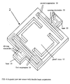
Fig. 6 shows a second embodiment of a micro yaw rate sensor, the sensor 2, made
in accordance with the principles of the present invention. The number of suspension
beams have been doubled in this embodiment to increase the efficiency of the driving
force as well as to increase the sensitivity to the Coriolis force. As with the first
embodiment, the driving electrodes are a pair of thin wires double side patterned on the
first suspension beam. However, the length of the electrodes have been extended to cover
the extra beam of the suspension. The serpentine shape electrodes are designed to create
two opposite bending moments at different sections of the beam along longitudinal
direction. The extra sensing electrodes provide additional information for functional
enhancement of the sensor, such as close loop driving resonance control, acceleration
detection and cancellation, etc.
-
The dimension of each sensor chip varies from hundreds of microns to thousands
of microns, and the wafer thickness ranges from tens of microns to hundreds of microns.
Generally, smaller sensors tend to be better in dynamics but large sensors tend to be
higher in sensitivity.
-
Fabrication of typical quartz sensors of present invention, such as embodiments 1
and 2 presents no particular difficulty to those who are familiar with the arts of modem
lithographic micro-machining technique. A typical fabrication process is only described
here as an example of micromachining technology for ease of reference. The process
follows: (a) depositing a thin Au/Cr layer on the wafer; (b) coating a photoresist on the
wafer; (c) patterning (i.e. exposing and developing) the shape of resonator on photoresist
with mask #1, a resonator shape mask; (d) patterning the shape of resonator on Au/Cr
coat; (e) bulk-etching the shape of resonator out of the wafer; (f) coating a layer of
photoresist; (g) patterning electrodes and electric connection pads with mask #2, an
electrodes mask; (h) patterning the electrodes on the Au/Cr layer.
-
The above process is usually performed on both sides of the wafer simultaneously
for manufacturing efficiency. And it should be apparent to those who are familiar with the
arts that the sensors of present invention can be batch fabricated with very simple
processes, and can be mass-produced more inexpensively in comparison with micro yaw
rate sensors of the prior art.
-
Alternatively, conventional methods can also be used in fabrication of the sensors
if the number of the sensors needed is too small to take advantage of the micromachining
technology and the tools to machine the sensor structure are available.
-
It should be noted that, although the sensor of present invention uses the same
quartz wafer as some of the tuning fork type yaw rate sensors of the prior art, they are
totally different in resonator structure and have two significant difference in design
principles. First, the tuning fork type is designed with surface electrodes, which cover two
of the four surfaces of a rectangular beam, including side wall surfaces. The surface
electrodes may produce stronger driving forces than the thin wire electrodes used in
present invention do, but the side wall electrodes cannot be fabricated with commonly
used micromachining equipment at low cost, and have less dimensional accuracy.
Second, the tuning fork type sensors of the prior art require two tine resonators vibrating
in opposite direction, while the sensor of present invention can operate with only one
resonator which reduces sophistication in fabrication and signal processing circuitry and
further lowers the cost of the sensor significantly.
-
Moreover, the sensor of the present invention uses a separate proof mass which
can be used to adjust the dynamics of the resonator and subsequently the sensitivity and
the dynamic range of the sensors. In comparison the tuning fork type sensors of the prior
art use tines as both suspension and proof mass, so the dynamics of the tuning fork is
decided by the length of the tine and the thickness of the wafer. In other words, the
sensors of the tuning forks allow a designer only a limited range to adjust its sensitivity
and dynamic range. Moreover, the packaging and mounting of sensors of the present
invention has little effect on the resonator performance while the mounting of the tuning
fork type sensors often is very critical to their performance, and requires frequently
patented special mounting techniques.
-
In addition to the basic simple embodiments, the sensors can be modified by:
- a) adding a single Y beam cantilever with the thin wire electrodes as sensing electrodes,
on the same base wafer side by side with the sensor resonator, to upgrade the yaw rate
sensor with an integrated two dimensional accelerometer.
- b) adding extra signal processing circuits to calculate the acceleration so as to upgrade the
yaw rate sensor with an integrated two dimensional accelerometer.
- c) adding an extra resonator to further improve the resistance to external shock and
mechanical noise.
- d) further adding extra beams in the suspension of the resonator to have higher
piezoelectric driving efficiency.
- e) exchanging, with slightly modified electrodes layout, the out of plane resonance to
driving resonance and in wafer plane resonance to sensing resonance.
-
-
It should be noted, that these modification will, presumably, add special features
or will enhance the usefulness of the sensor in various industrial application, but they
make the sensors more sophisticated and more expensive to manufacture. For practical
use, an optimal shape of the driving electrodes and suspension beams is one which will
minimize the driving power while creating a steady driving resonance and a highly
sensitive sensing resonance.
-
In an industrial application, the driving and sensing circuits for the sensors of the
present invention should be modularized and integrated on a single chip for ease of use.
The sensor chip, or the base wafer, can be directly mounted on a printed circuit board or a
plastic package to lower the cost. Alternatively, it may be packaged in an vacuum
package to increase the sensitivity and to lower thermal noise.
-
In conclusion, the present invention provides micro yaw rate sensors which have
the following desirable characteristics: (a) a simple structure; (b) easy to fabricate with
common micromachining equipment; (c) operatable at wide temperature range with good
temperature stability; (d) a linear response; (e) easy to process readout signal; (f) easy to
package; (g) good long term stability; (h) easy to adjust sensitivity and dynamic range
with dimensional change without change quartz wafer and fabrication equipment. In
summary, the sensor structure are suitable for fabrication with micro-machining
techniques commonly used in the semiconductor industry, and they are inexpensive to
manufacture.