EP0948805B1 - Wafer electrical discharge control - Google Patents
Wafer electrical discharge control Download PDFInfo
- Publication number
- EP0948805B1 EP0948805B1 EP97952388A EP97952388A EP0948805B1 EP 0948805 B1 EP0948805 B1 EP 0948805B1 EP 97952388 A EP97952388 A EP 97952388A EP 97952388 A EP97952388 A EP 97952388A EP 0948805 B1 EP0948805 B1 EP 0948805B1
- Authority
- EP
- European Patent Office
- Prior art keywords
- substrate
- arrangement
- lifting
- chuck
- electrically conductive
- Prior art date
- Legal status (The legal status is an assumption and is not a legal conclusion. Google has not performed a legal analysis and makes no representation as to the accuracy of the status listed.)
- Expired - Lifetime
Links
Images



Classifications
-
- H—ELECTRICITY
- H01—ELECTRIC ELEMENTS
- H01J—ELECTRIC DISCHARGE TUBES OR DISCHARGE LAMPS
- H01J37/00—Discharge tubes with provision for introducing objects or material to be exposed to the discharge, e.g. for the purpose of examination or processing thereof
- H01J37/32—Gas-filled discharge tubes
- H01J37/32431—Constructional details of the reactor
-
- H—ELECTRICITY
- H10—SEMICONDUCTOR DEVICES; ELECTRIC SOLID-STATE DEVICES NOT OTHERWISE PROVIDED FOR
- H10P—GENERIC PROCESSES OR APPARATUS FOR THE MANUFACTURE OR TREATMENT OF DEVICES COVERED BY CLASS H10
- H10P72/00—Handling or holding of wafers, substrates or devices during manufacture or treatment thereof
- H10P72/50—Handling or holding of wafers, substrates or devices during manufacture or treatment thereof for positioning, orientation or alignment
-
- H—ELECTRICITY
- H02—GENERATION; CONVERSION OR DISTRIBUTION OF ELECTRIC POWER
- H02N—ELECTRIC MACHINES NOT OTHERWISE PROVIDED FOR
- H02N13/00—Clutches or holding devices using electrostatic attraction, e.g. using Johnson-Rahbek effect
-
- H—ELECTRICITY
- H10—SEMICONDUCTOR DEVICES; ELECTRIC SOLID-STATE DEVICES NOT OTHERWISE PROVIDED FOR
- H10P—GENERIC PROCESSES OR APPARATUS FOR THE MANUFACTURE OR TREATMENT OF DEVICES COVERED BY CLASS H10
- H10P72/00—Handling or holding of wafers, substrates or devices during manufacture or treatment thereof
- H10P72/70—Handling or holding of wafers, substrates or devices during manufacture or treatment thereof for supporting or gripping
- H10P72/72—Handling or holding of wafers, substrates or devices during manufacture or treatment thereof for supporting or gripping using electrostatic chucks
-
- H—ELECTRICITY
- H10—SEMICONDUCTOR DEVICES; ELECTRIC SOLID-STATE DEVICES NOT OTHERWISE PROVIDED FOR
- H10P—GENERIC PROCESSES OR APPARATUS FOR THE MANUFACTURE OR TREATMENT OF DEVICES COVERED BY CLASS H10
- H10P72/00—Handling or holding of wafers, substrates or devices during manufacture or treatment thereof
- H10P72/70—Handling or holding of wafers, substrates or devices during manufacture or treatment thereof for supporting or gripping
- H10P72/72—Handling or holding of wafers, substrates or devices during manufacture or treatment thereof for supporting or gripping using electrostatic chucks
- H10P72/722—Details of electrostatic chucks
-
- Y—GENERAL TAGGING OF NEW TECHNOLOGICAL DEVELOPMENTS; GENERAL TAGGING OF CROSS-SECTIONAL TECHNOLOGIES SPANNING OVER SEVERAL SECTIONS OF THE IPC; TECHNICAL SUBJECTS COVERED BY FORMER USPC CROSS-REFERENCE ART COLLECTIONS [XRACs] AND DIGESTS
- Y10—TECHNICAL SUBJECTS COVERED BY FORMER USPC
- Y10S—TECHNICAL SUBJECTS COVERED BY FORMER USPC CROSS-REFERENCE ART COLLECTIONS [XRACs] AND DIGESTS
- Y10S156/00—Adhesive bonding and miscellaneous chemical manufacture
- Y10S156/915—Differential etching apparatus including focus ring surrounding a wafer for plasma apparatus
Definitions
- the present invention relates to the handling of a substrate in the manufacture of an integrated circuit. More particularly, the present invention relates to an apparatus for controllably discharging an electrical charge remaining on a substrate in a plasma processing chamber during wafer processing.
- Substrates such as semiconductor substrates or glass substrates, are typically processed using plasma processing chambers to perform various process steps during the manufacture of the resultant devices, e.g., integrated circuits or flat panel displays.
- plasma processing chambers to perform various process steps during the manufacture of the resultant devices, e.g., integrated circuits or flat panel displays.
- These plasma-enhanced semiconductor processes are well known to those skilled in the art.
- An important aspect of this manufacturing process is the handling of the substrate during its overall processing. Typically the handling and transport of the substrate from one particular process to another is highly automated. As is known, one of the steps that is typically automated is the removing of the substrate from a plasma processing chamber after the processing of the substrate within the chamber.
- WO-A-95/24764 discloses an electrostatic conductor wherein a voltage of the same polarity as the workpiece is applied to the chuck.
- JP-A-05275517 discloses an arrangement wherein the substrate is detached from the chuck by earthed lifting pins or by ejecting compressed gas between the substrate and chuck.
- JP-A-06338463 discloses an arrangement including a susceptor for placing the wafer, a lifting pin for releasing the wafer from the susceptor and a resistance for gradually discharging charges on the wafer.
- FIG. 1 illustrates typical plasma processing system 100 having a plasma processing chamber 102.
- Chamber 102 includes a base plate 104 and an electrostatic chuck 106 for supporting a substrate 108 during the processing of the substrate.
- a substrate lifting arrangement 109 includes an actuator 110 and a lifting mechanism 112 having three or more, e.g., four, lifting pins 114.
- the various components making up the lifting arrangement 109 are typically electrically conductive and lifting arrangement 109 is typically electrically connected to ground when there is no power to the chuck.
- electrostatic chuck 106 includes a layer of dielectric material 116 for electrically insulating chuck 106 from substrate 108.
- Actuator 110 is arranged to move lifting mechanism 112 between a first position in which lifting pins 114 do not engage substrate 108 and a second position in which lifting pins 114 engage and lift substrate 108 off chuck 106.
- the substrate In order to remove the substrate from the plasma processing chamber, the substrate is typically lifted from the chuck using a substrate lifting arrangement such as substrate lifting arrangement 109 described above.
- a substrate lifting arrangement such as substrate lifting arrangement 109 described above.
- the substrate may tend to stick to the chuck.
- this sticking problem is caused by an electrical charge which remains on the substrate after the processing of the substrate.
- the substrate sticks to the chuck, the substrate may have a tendency to pop loose from the chuck as the lifting arrangement lifts the substrate. This popping off may cause the substrate to be displaced relative to its expected position for grasping by the transport mechanism. If the substrate is not in its proper location, the transport mechanism may not be able to properly grasp the substrate and the overall system will have to be stopped so that the displaced substrate can be manually retrieved.
- an additional step is added to the processing of the substrate within the plasma processing chamber.
- This additional step referred to as plasma discharging, involves striking a plasma within the chamber which acts as a conductive path for the charge on the substrate to discharge to the wall of the chamber.
- plasma discharging involves striking a plasma within the chamber which acts as a conductive path for the charge on the substrate to discharge to the wall of the chamber.
- this approach increases the processing time required to process the substrate within the chamber and reduces the throughput of the overall process thereby increasing the overall costs involved with using this approach.
- this process is typically not able to fully discharge the substrate and therefore does not eliminate the potential for the sticking problem.
- the lifting arrangement is electrically conductive and grounded as described above for Figure 1. With this arrangement, when the lifting arrangement engages the substrate, any charge remaining on the substrate is discharged through the substrate lifting arrangement. Although this approach does not require any additional process steps and eliminates the sticking problem, in some cases, this approach may cause damage to portions of the substrate. This damage may be caused when relatively high voltage currents are concentrated into small areas of the substrate which are in direct contact with the grounded lifting pins. Although this damage may not occur for substrates having relatively thick oxide layers, as the oxide layers of the substrate get thinner and thinner in order to increase the density of components on the substrate and/or to improve device performance, damage due to these concentrated currents is more likely.
- the present invention provides an apparatus for controlling the discharge of any electrical charge remaining on a substrate as the substrate is lifted by a lifting arrangement from a chuck. This avoids the sticking problem while also minimizing the chances of damaging the substrate due to high voltage currents concentrated through small areas of the substrate which are in direct contact with the lifting arrangement.
- the substrate In order to remove the substrate from the plasma processing chamber, the substrate is typically lifted from the chuck using a substrate lifting arrangement such as substrate lifting arrangement 109 described above.
- a substrate lifting arrangement such as substrate lifting arrangement 109 described above.
- the substrate may tend to stick to the chuck.
- this sticking problem is caused by an electrical charge which remains on the substrate after the processing of the substrate.
- the substrate sticks to the chuck, the substrate may have a tendency to pop loose from the chuck as the lifting arrangement lifts the substrate. This popping off may cause the substrate to be displaced relative to its expected position for grasping by the transport mechanism. If the substrate is not in its proper location, the transport mechanism may not be able to properly grasp the substrate and the overall system will have to be stopped so that the displaced substrate can be manually retrieved.
- An invention for providing, in a plasma processing chamber, an apparatus for controlling the discharge of any electrical charge remaining on a substrate as the substrate is engaged and lifted by a lifting arrangement.
- numerous specific details are set forth in order to provide a thorough understanding of the present invention. It will be obvious, however, to one skilled in the art, that the present invention may be embodied in a wide variety of specific configurations. Also, well known processes have not been described in detail in order not to unnecessarily obscure the present invention.
- the inventive substrate discharging technique may be performed in any known plasma processing apparatuses such as, but not limited to, those adapted for dry etching, plasma etching, reactive ion etching, magnetically enhanced reactive ion etching, electron cyclotron resonance or the like. Note that this is true irrespective of whether energy to the plasma is delivered through capacitively coupled parallel electrode plates, through E.R. microwave plasma sources, or through inductively coupled RF sources such as helicon, helical resonators, and transformer coupled plasma. These processing systems, among others, are readily available commercially.
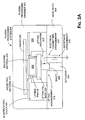
- FIG. 2A illustrates a simplified schematic of a plasma processing system 200 designed in accordance with the present invention.
- system 200 has a plasma processing chamber 202 including a base plate 204 and an electrostatic chuck 206 for supporting a substrate 208 during the processing of the substrate.
- Electrostatic chuck 206 includes a layer of dielectric material 210 for electrically insulating chuck 206 from substrate 208.
- a substrate lifting arrangement 212 includes an actuator 214 and a lifting mechanism 216.
- Lifting mechanism 216 has lifting pins 218, a lifting pin base 220, and a shaft 222. Lifting pins 218 are supported by base 220 which in turn is supported by shaft 222.
- Actuator 214 arranged to move lifting mechanism 216 between a first position in which lifting pins 218 do not engage substrate 208 and a second position in which lifting pins 218 extend through chuck 206 and engage and lift substrate 208 off chuck 206.
- lifting arrangement 212 has been described as having a specific configuration, it is to be understood that the lifting arrangement may take on a wide variety of forms so long as it is capable of lifting substrate 208 off chuck 206.
- lifting arrangement 212 includes an electrical connecting arrangement 224 that electrically connects the substrate to ground through a resistance arrangement 226 when lifting arrangement 212 engages and lifts substrate 208 off chuck 206.
- Resistance arrangement 226 is configured to have a predetermined resistance. With this configuration, any electrical charge that remains on substrate 208 is discharged through electrical connecting arrangement 224 and resistance arrangement 226. Resistance arrangement 226 limits the current flow through electrical connecting arrangement 224 hereby controlling the discharge of any charge remaining on substrate 208.
- resistance arrangement 226 In order to avoid the sticking problem, resistance arrangement 226 must be designed to have a resistance low enough that it allows the charge remaining on the substrate to be discharged quickly enough to avoid large sticking forces. However, the resistance must also be kept high enough to limit the current flow enough to minimize the potential for damage to portions of the substrate due to high voltage currents concentrated through small areas of the substrate which are in direct contact with the lifting arrangement.
- Figure 2B and 2C respectively illustrate substrate 208 just before it is to be lifted and as it is beginning to be lifted off chuck 206.
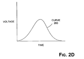
- Figure 2D is a graph illustrating the relationship between the voltage due to charge on substrate 208 and time as the substrate is being lifted from chuck 206.
- the charge (indicated by reference letter Q) on the substrate is equal to the capacitance (indicated by the reference letter C) of substrate 208 relative to chuck 206 and the voltage differential (indicated by the reference letter V) between the substrate and the chuck.
- the capacitance (C) is proportional to the area and the distance between the substrate and the chuck. As the area between the substrate and the chuck decreases and the distance between the substrate and the chuck increases, the capitance (C) decreases. Therefore, as the area decreases and the distance increases, the voltage associated with the charge on the substrate increases as required by formula 250.
- the sticking force which attracts and holds substrate 208 against chuck 206 is proportional to the square of the voltage (V).
- V voltage
- the area of contact between the substrate and the chuck decreased and the distance between the substrate and the chuck is increased.
- These voltages may reach voltages as high as 1 K Volt.
- the increase in the voltage also causes an increase in the sticking force of the substrate to the chuck due to the fact that sticking force is proportional to the square of the voltage.
- lifting arrangement 212 also electrically connects the substrate to ground through resistance arrangement 226, the charge (Q) on substrate 208 causes a current to flow through resistance arrangement 226 thereby reducing the charge (Q) on substrate 208 relative to time.
- the reduction of the charge over time reduces the voltage over time as required by formula 250 of Figure 2B and as indicated by the downward portion of curve 260 of Figure 2D.
- resistance of resistance arrangement 226 controls how much current flows from the substrate to ground, this resistance determines how long it takes to discharge any charge remaining on substrate 208. As indicated above, the resistance must be kept high enough to limit the current flow enough to minimize the potential damage to portions of the substrate due to high voltage currents concentrated through small areas of the substrate which are in direct contact with the lifting arrangement. However, the resistance must also be small enough to allow the charge remaining on the substrate to be discharged quickly enough to avoid large sticking forces. It should be noted that the speed at which lifting arrangement 212 lifts substrate 208 off chuck 206 determines the rate of change of the capacitance and therefore the rate of change of the sticking force. For this reason, slowing down the speed at which the lifting arrangement lifts the substrate increases the available discharge time, that is, the amount of time available to discharge the charge remaining on substrate 208 and thereby reduce the sticking forces.
- the above described relationships may be used to determine a wide variety of useful desired resistances for resistance arrangement 226 depending on the charge (Q) that remains on the substrate after processing of the substrate within the chamber and depending on the speed at which the substrate is lifted by lifting arrangement 212. Because of the multiple variables involved (i.e. charge, lifting speed, and resistance), an wide variety of solutions are available. However, for a given charge and a given lifting speed, one skilled in the art may easily determine a useful resistance in view of the above description.
- a resistance of 10 M ⁇ was used for resistance arrangement 226.
- a conventional actuator was used to move lifting arrangement 212 in order to lift the substrate off the chuck.
- the discharge time associated with this configuration was measured to be approximately 1/10 th of a second.
- all of the components making up the lifting arrangement are electrically conductive. That is, lifting pins 218 which are supported by lifting pin base 220 which is in turn supported by shaft 222 are all electrically conductive.
- shaft 222 of the lifting arrangement 216 is not directly connected to ground. Instead, shaft 222 is electrically connected to ground through a variable resistance resistor 602. This arrangement allows the resistance of variable resistance resistor 602 to be changed to suit the specific requirements for the particular substrate being processed in the plasma processing chamber.
- variable resistance resistor 602 is automatically controlled by a suitable and readily available controller 604.
- Controller 604 may be programmed to set the resistance of resistor 602 to predetermined resistances based on the process steps used in processing the substrate. This configuration allows the system to automatically change the resistance of resistor 602 to predetermined settings for different substrate process.
- the substrate lifting arrangement of the above described embodiments has been described as having a specific configuration including four lifting pins, a base, and a shaft which is moved by an actuator, it should be understood that the lifting arrangement may take on a wide variety of specific configurations and still remain within the scope of the invention. In fact, the invention would equally apply to any lifting arrangement configuration that would be capable of lifting arrangement configuration that would be capable of lifting the substrate from the chuck while being electrically connected to ground through a predetermined resistance as described above.
- the lifting arrangement may have any number of lifting pins, or for that matter, may use elements other than lifting pins to engage the substrate.
- the actuator may take a wide variety of forms so long as the actuator causes the engaging elements of the lifting arrangement to engage and lift the substrate off the chuck.
Landscapes
- Physics & Mathematics (AREA)
- Engineering & Computer Science (AREA)
- Plasma & Fusion (AREA)
- Chemical & Material Sciences (AREA)
- Analytical Chemistry (AREA)
- Container, Conveyance, Adherence, Positioning, Of Wafer (AREA)
- Dowels (AREA)
- Cold Cathode And The Manufacture (AREA)
- Mechanical Treatment Of Semiconductor (AREA)
- Electrical Discharge Machining, Electrochemical Machining, And Combined Machining (AREA)
- Drying Of Semiconductors (AREA)
Abstract
Description
Claims (2)
- A substrate lifting arrangement for use in a plasma processing chamber (202) having an electrostatic chuck (206) configured for supporting a substrate (208) during processing of said substrate within said plasma processing chamber, said substrate lifting arrangement comprising:characterised in that said resistance arrangement comprises a variable resistor connected between the shaft and said ground and which is designed to have a predetermined resistance high enough to limit the current flow to minimize the potential for damage to portions of the substrate due to high voltage currents concentrated through small areas of the substrate which are in direct contact with the lifting pins, and small enough to allow the charge remaining in the substrate to be discharged quickly to avoid large sticking forces.a plurality of electrically conductive lifting pins (218) movable between a first position in which said plurality of electrically conductive lifting pins does not engage said substrate and a second position in which said plurality of electrically conductive lifting pins engages said substrate and lifts said substrate off said chuck;a base (204) supporting said plurality of electrically conductive lifting pins and movable between said first and second positions;an electrically conductive shaft (222) supporting said base, wherein each of the plurality of said electrically conductive lifting pins is electrically connected to said conductive shaft, and wherein said conductive shaft is movable between said first and second positions and wherein said conductive shaft is electrically coupled to ground;an actuator (214) coupled to said conductive shaft, said actuator controlling movement of said conductive shaft between said first and second positions; anda resistance arrangement (226) coupled between said plurality of electrically conductive lifting pins and said ground through said conductive shaft, said resistance arrangement limiting a current flowing from said substrate to ground through said resistance arrangement, said current being caused by remaining electrical charge on said substrate when said substrate is lifted off said chuck by said plurality of electrically conductive lifting pins,
- The substrate lifting arrangement, as recited in claim 1, wherein said plurality of electrically conductive lifting pins comprises at least four electrically conductive lifting pins (218).
Priority Applications (1)
| Application Number | Priority Date | Filing Date | Title |
|---|---|---|---|
| EP04006189A EP1435646B1 (en) | 1996-12-19 | 1997-12-18 | Wafer electrical discharge control by wafer lifter system |
Applications Claiming Priority (3)
| Application Number | Priority Date | Filing Date | Title |
|---|---|---|---|
| US08/769,433 US5904779A (en) | 1996-12-19 | 1996-12-19 | Wafer electrical discharge control by wafer lifter system |
| US769433 | 1996-12-19 | ||
| PCT/US1997/022799 WO1998027577A1 (en) | 1996-12-19 | 1997-12-18 | Wafer electrical discharge control by wafer lifter system |
Related Child Applications (1)
| Application Number | Title | Priority Date | Filing Date |
|---|---|---|---|
| EP04006189A Division EP1435646B1 (en) | 1996-12-19 | 1997-12-18 | Wafer electrical discharge control by wafer lifter system |
Publications (2)
| Publication Number | Publication Date |
|---|---|
| EP0948805A1 EP0948805A1 (en) | 1999-10-13 |
| EP0948805B1 true EP0948805B1 (en) | 2005-07-06 |
Family
ID=25085430
Family Applications (2)
| Application Number | Title | Priority Date | Filing Date |
|---|---|---|---|
| EP97952388A Expired - Lifetime EP0948805B1 (en) | 1996-12-19 | 1997-12-18 | Wafer electrical discharge control |
| EP04006189A Expired - Lifetime EP1435646B1 (en) | 1996-12-19 | 1997-12-18 | Wafer electrical discharge control by wafer lifter system |
Family Applications After (1)
| Application Number | Title | Priority Date | Filing Date |
|---|---|---|---|
| EP04006189A Expired - Lifetime EP1435646B1 (en) | 1996-12-19 | 1997-12-18 | Wafer electrical discharge control by wafer lifter system |
Country Status (7)
| Country | Link |
|---|---|
| US (1) | US5904779A (en) |
| EP (2) | EP0948805B1 (en) |
| JP (1) | JP4101299B2 (en) |
| KR (1) | KR20000057603A (en) |
| AT (2) | ATE389946T1 (en) |
| DE (2) | DE69733697T2 (en) |
| WO (1) | WO1998027577A1 (en) |
Families Citing this family (26)
| Publication number | Priority date | Publication date | Assignee | Title |
|---|---|---|---|---|
| US5955858A (en) | 1997-02-14 | 1999-09-21 | Applied Materials, Inc. | Mechanically clamping robot wrist |
| JPH10284360A (en) | 1997-04-02 | 1998-10-23 | Hitachi Ltd | Substrate temperature control device and method |
| US6177023B1 (en) * | 1997-07-11 | 2001-01-23 | Applied Komatsu Technology, Inc. | Method and apparatus for electrostatically maintaining substrate flatness |
| JP3374743B2 (en) * | 1998-03-05 | 2003-02-10 | 日本電気株式会社 | Substrate heat treatment apparatus and method of separating substrate from the apparatus |
| US6146504A (en) * | 1998-05-21 | 2000-11-14 | Applied Materials, Inc. | Substrate support and lift apparatus and method |
| JP4394778B2 (en) * | 1999-09-22 | 2010-01-06 | 東京エレクトロン株式会社 | Plasma processing apparatus and plasma processing method |
| KR100503897B1 (en) * | 2000-02-19 | 2005-07-25 | 엘지.필립스 엘시디 주식회사 | Method for preventing damage of a substrate while performing a dry etching and apparatus the same |
| JP3549188B2 (en) | 2000-03-27 | 2004-08-04 | 日本エー・エス・エム株式会社 | Method for forming thin film on semiconductor substrate |
| KR100378187B1 (en) * | 2000-11-09 | 2003-03-29 | 삼성전자주식회사 | A wafer stage including electro-static chuck and method for dechucking wafer using the same |
| US6646857B2 (en) * | 2001-03-30 | 2003-11-11 | Lam Research Corporation | Semiconductor wafer lifting device and methods for implementing the same |
| US6673636B2 (en) | 2001-05-18 | 2004-01-06 | Applied Materails Inc. | Method of real-time plasma charging voltage measurement on powered electrode with electrostatic chuck in plasma process chambers |
| KR100995715B1 (en) * | 2002-04-09 | 2010-11-19 | 파나소닉 주식회사 | Plasma treatment method and apparatus and plasma treatment tray |
| JP2005064284A (en) * | 2003-08-14 | 2005-03-10 | Asm Japan Kk | Semiconductor substrate holding device |
| US7013956B2 (en) * | 2003-09-02 | 2006-03-21 | Thermal Corp. | Heat pipe evaporator with porous valve |
| US7129731B2 (en) * | 2003-09-02 | 2006-10-31 | Thermal Corp. | Heat pipe with chilled liquid condenser system for burn-in testing |
| US20050067146A1 (en) * | 2003-09-02 | 2005-03-31 | Thayer John Gilbert | Two phase cooling system method for burn-in testing |
| US20050067147A1 (en) * | 2003-09-02 | 2005-03-31 | Thayer John Gilbert | Loop thermosyphon for cooling semiconductors during burn-in testing |
| KR20070072571A (en) * | 2004-11-04 | 2007-07-04 | 가부시키가이샤 알박 | Electrostatic chuck device |
| CN100362645C (en) * | 2005-12-07 | 2008-01-16 | 北京北方微电子基地设备工艺研究中心有限责任公司 | Thimble device |
| US8270142B2 (en) * | 2008-12-10 | 2012-09-18 | Axcelis Technologies, Inc. | De-clamping wafers from an electrostatic chuck |
| US8360844B2 (en) * | 2010-03-13 | 2013-01-29 | Marc B Schwartz | Multiple wager, multiple potential winning outcome gaming platform |
| US9595464B2 (en) * | 2014-07-19 | 2017-03-14 | Applied Materials, Inc. | Apparatus and method for reducing substrate sliding in process chambers |
| US11387135B2 (en) * | 2016-01-28 | 2022-07-12 | Applied Materials, Inc. | Conductive wafer lift pin o-ring gripper with resistor |
| US20190088518A1 (en) * | 2017-09-20 | 2019-03-21 | Applied Materials, Inc. | Substrate support with cooled and conducting pins |
| KR102547860B1 (en) | 2020-08-10 | 2023-06-23 | 세메스 주식회사 | Substrate supporting member, substrate treating apparatus including the same and substrate treating method thereof |
| CN115250648B (en) * | 2021-02-25 | 2025-11-11 | 株式会社日立高新技术 | Plasma processing apparatus |
Family Cites Families (17)
| Publication number | Priority date | Publication date | Assignee | Title |
|---|---|---|---|---|
| EP0439000B1 (en) * | 1990-01-25 | 1994-09-14 | Applied Materials, Inc. | Electrostatic clamp and method |
| JP3230821B2 (en) * | 1991-01-28 | 2001-11-19 | 株式会社東芝 | Electrostatic chuck with pusher pin |
| JP3182615B2 (en) * | 1991-04-15 | 2001-07-03 | アネルバ株式会社 | Plasma processing method and apparatus |
| JP3027781B2 (en) * | 1992-02-13 | 2000-04-04 | 東京エレクトロン株式会社 | Plasma processing method |
| JPH05275517A (en) * | 1992-03-30 | 1993-10-22 | Fujitsu Ltd | Substrate detaching method |
| JP3264391B2 (en) * | 1993-05-17 | 2002-03-11 | 東京エレクトロン株式会社 | Removal device for electrostatic attraction |
| US5557215A (en) * | 1993-05-12 | 1996-09-17 | Tokyo Electron Limited | Self-bias measuring method, apparatus thereof and electrostatic chucking apparatus |
| JPH06338463A (en) * | 1993-05-28 | 1994-12-06 | Toshiba Corp | Semiconductor manufacturing equipment |
| JPH077072A (en) * | 1993-06-17 | 1995-01-10 | Anelva Corp | Substrate attachment / detachment method and attachment / detachment mechanism in electrostatic chuck device |
| JP2817585B2 (en) * | 1993-09-10 | 1998-10-30 | 住友金属工業株式会社 | Sample removal method |
| US5463525A (en) * | 1993-12-20 | 1995-10-31 | International Business Machines Corporation | Guard ring electrostatic chuck |
| US5535507A (en) * | 1993-12-20 | 1996-07-16 | International Business Machines Corporation | Method of making electrostatic chuck with oxide insulator |
| US5467249A (en) * | 1993-12-20 | 1995-11-14 | International Business Machines Corporation | Electrostatic chuck with reference electrode |
| US5459632A (en) * | 1994-03-07 | 1995-10-17 | Applied Materials, Inc. | Releasing a workpiece from an electrostatic chuck |
| JP3608121B2 (en) * | 1994-03-18 | 2005-01-05 | アネルバ株式会社 | Mechanical desorption mechanism of substrate and desorption method using the mechanism |
| JPH08107139A (en) * | 1994-10-05 | 1996-04-23 | Hitachi Ltd | Insulating ring member and semiconductor manufacturing apparatus using the same |
| JPH08236601A (en) * | 1995-02-22 | 1996-09-13 | Mitsubishi Electric Corp | Electrostatic chuck device |
-
1996
- 1996-12-19 US US08/769,433 patent/US5904779A/en not_active Expired - Lifetime
-
1997
- 1997-12-18 AT AT04006189T patent/ATE389946T1/en not_active IP Right Cessation
- 1997-12-18 JP JP52783698A patent/JP4101299B2/en not_active Expired - Fee Related
- 1997-12-18 DE DE69733697T patent/DE69733697T2/en not_active Expired - Lifetime
- 1997-12-18 EP EP97952388A patent/EP0948805B1/en not_active Expired - Lifetime
- 1997-12-18 EP EP04006189A patent/EP1435646B1/en not_active Expired - Lifetime
- 1997-12-18 DE DE69738590T patent/DE69738590T2/en not_active Expired - Lifetime
- 1997-12-18 KR KR1019990705387A patent/KR20000057603A/en not_active Ceased
- 1997-12-18 WO PCT/US1997/022799 patent/WO1998027577A1/en not_active Ceased
- 1997-12-18 AT AT97952388T patent/ATE299293T1/en not_active IP Right Cessation
Also Published As
| Publication number | Publication date |
|---|---|
| JP2001506808A (en) | 2001-05-22 |
| EP1435646A3 (en) | 2006-05-10 |
| DE69733697T2 (en) | 2006-05-24 |
| WO1998027577A1 (en) | 1998-06-25 |
| EP1435646B1 (en) | 2008-03-19 |
| KR20000057603A (en) | 2000-09-25 |
| EP0948805A1 (en) | 1999-10-13 |
| DE69738590D1 (en) | 2008-04-30 |
| ATE389946T1 (en) | 2008-04-15 |
| US5904779A (en) | 1999-05-18 |
| DE69733697D1 (en) | 2005-08-11 |
| DE69738590T2 (en) | 2009-04-23 |
| JP4101299B2 (en) | 2008-06-18 |
| ATE299293T1 (en) | 2005-07-15 |
| EP1435646A2 (en) | 2004-07-07 |
Similar Documents
| Publication | Publication Date | Title |
|---|---|---|
| EP1435646B1 (en) | Wafer electrical discharge control by wafer lifter system | |
| US6646857B2 (en) | Semiconductor wafer lifting device and methods for implementing the same | |
| TWI301311B (en) | Method and apparatus for dechucking a substrate | |
| US4624728A (en) | Pin lift plasma processing | |
| US5460684A (en) | Stage having electrostatic chuck and plasma processing apparatus using same | |
| US8277673B2 (en) | Plasma processing method and apparatus | |
| US5997962A (en) | Plasma process utilizing an electrostatic chuck | |
| WO2006049085A1 (en) | Electrostatic chuck apparatus | |
| JP2879887B2 (en) | Plasma processing method | |
| US11107694B2 (en) | Method for releasing sample and plasma processing apparatus using same | |
| KR101980994B1 (en) | Substrate processing device and substrate processing method | |
| US20080242086A1 (en) | Plasma processing method and plasma processing apparatus | |
| US12040216B2 (en) | Substrate supporting member, substrate treating apparatus including the same and substrate treating method thereof | |
| CN114388421A (en) | Method for adjusting contact position of lift pin, method for detecting contact position of lift pin, and substrate mounting mechanism | |
| KR100845896B1 (en) | Plasma treatment system and method for preventing arcing between an electrostatic chuck and a substrate to be processed | |
| JPH11330217A (en) | Method for separating substrate from surface of electrostatic chuck plate | |
| WO2025145925A1 (en) | Lower electrode system, semiconductor process device and control method | |
| Shan et al. | Process kit and wafer temperature effects on dielectric etch rate and uniformity of electrostatic chuck | |
| JP2001077186A (en) | Vacuum processing method | |
| JPH08274150A (en) | Electrostatic attracting stage | |
| JPH06244146A (en) | Plasma processing device | |
| KR20050092583A (en) | Apparatus and method for discharging remanent voltage of wafer in processe chamber | |
| KR20060077667A (en) | Electrostatic Chuck of Semiconductor Wafer | |
| KR20050049725A (en) | Electro static chuck for preventing sticking |
Legal Events
| Date | Code | Title | Description |
|---|---|---|---|
| PUAI | Public reference made under article 153(3) epc to a published international application that has entered the european phase |
Free format text: ORIGINAL CODE: 0009012 |
|
| AK | Designated contracting states |
Kind code of ref document: A1 Designated state(s): AT DE FR GB IE NL |
|
| 17P | Request for examination filed |
Effective date: 19990617 |
|
| 17Q | First examination report despatched |
Effective date: 20010518 |
|
| RTI1 | Title (correction) |
Free format text: WAFER ELECTRICAL DISCHARGE CONTROL |
|
| GRAP | Despatch of communication of intention to grant a patent |
Free format text: ORIGINAL CODE: EPIDOSNIGR1 |
|
| GRAS | Grant fee paid |
Free format text: ORIGINAL CODE: EPIDOSNIGR3 |
|
| GRAA | (expected) grant |
Free format text: ORIGINAL CODE: 0009210 |
|
| AK | Designated contracting states |
Kind code of ref document: B1 Designated state(s): AT DE FR GB IE NL |
|
| PG25 | Lapsed in a contracting state [announced via postgrant information from national office to epo] |
Ref country code: AT Free format text: LAPSE BECAUSE OF FAILURE TO SUBMIT A TRANSLATION OF THE DESCRIPTION OR TO PAY THE FEE WITHIN THE PRESCRIBED TIME-LIMIT Effective date: 20050706 |
|
| REG | Reference to a national code |
Ref country code: GB Ref legal event code: FG4D |
|
| REG | Reference to a national code |
Ref country code: IE Ref legal event code: FG4D |
|
| REF | Corresponds to: |
Ref document number: 69733697 Country of ref document: DE Date of ref document: 20050811 Kind code of ref document: P |
|
| PG25 | Lapsed in a contracting state [announced via postgrant information from national office to epo] |
Ref country code: GB Free format text: LAPSE BECAUSE OF NON-PAYMENT OF DUE FEES Effective date: 20051218 |
|
| PG25 | Lapsed in a contracting state [announced via postgrant information from national office to epo] |
Ref country code: IE Free format text: LAPSE BECAUSE OF NON-PAYMENT OF DUE FEES Effective date: 20051219 |
|
| ET | Fr: translation filed | ||
| PLBE | No opposition filed within time limit |
Free format text: ORIGINAL CODE: 0009261 |
|
| STAA | Information on the status of an ep patent application or granted ep patent |
Free format text: STATUS: NO OPPOSITION FILED WITHIN TIME LIMIT |
|
| 26N | No opposition filed |
Effective date: 20060407 |
|
| GBPC | Gb: european patent ceased through non-payment of renewal fee |
Effective date: 20051218 |
|
| REG | Reference to a national code |
Ref country code: IE Ref legal event code: MM4A |
|
| PGFP | Annual fee paid to national office [announced via postgrant information from national office to epo] |
Ref country code: NL Payment date: 20120103 Year of fee payment: 15 |
|
| REG | Reference to a national code |
Ref country code: NL Ref legal event code: V1 Effective date: 20130701 |
|
| PG25 | Lapsed in a contracting state [announced via postgrant information from national office to epo] |
Ref country code: NL Free format text: LAPSE BECAUSE OF NON-PAYMENT OF DUE FEES Effective date: 20130701 |
|
| REG | Reference to a national code |
Ref country code: FR Ref legal event code: PLFP Year of fee payment: 19 |
|
| PGFP | Annual fee paid to national office [announced via postgrant information from national office to epo] |
Ref country code: FR Payment date: 20151217 Year of fee payment: 19 |
|
| PGFP | Annual fee paid to national office [announced via postgrant information from national office to epo] |
Ref country code: DE Payment date: 20151229 Year of fee payment: 19 |
|
| REG | Reference to a national code |
Ref country code: DE Ref legal event code: R119 Ref document number: 69733697 Country of ref document: DE |
|
| REG | Reference to a national code |
Ref country code: FR Ref legal event code: ST Effective date: 20170831 |
|
| PG25 | Lapsed in a contracting state [announced via postgrant information from national office to epo] |
Ref country code: FR Free format text: LAPSE BECAUSE OF NON-PAYMENT OF DUE FEES Effective date: 20170102 |
|
| PG25 | Lapsed in a contracting state [announced via postgrant information from national office to epo] |
Ref country code: DE Free format text: LAPSE BECAUSE OF NON-PAYMENT OF DUE FEES Effective date: 20170701 |