EP0948038B1 - Method of fabricating an avalanche diode with controllable threshold - Google Patents
Method of fabricating an avalanche diode with controllable threshold Download PDFInfo
- Publication number
- EP0948038B1 EP0948038B1 EP99410025A EP99410025A EP0948038B1 EP 0948038 B1 EP0948038 B1 EP 0948038B1 EP 99410025 A EP99410025 A EP 99410025A EP 99410025 A EP99410025 A EP 99410025A EP 0948038 B1 EP0948038 B1 EP 0948038B1
- Authority
- EP
- European Patent Office
- Prior art keywords
- region
- substrate
- avalanche
- regions
- conductivity type
- Prior art date
- Legal status (The legal status is an assumption and is not a legal conclusion. Google has not performed a legal analysis and makes no representation as to the accuracy of the status listed.)
- Expired - Lifetime
Links
- 238000004519 manufacturing process Methods 0.000 title claims description 15
- 239000000758 substrate Substances 0.000 claims description 27
- 238000009792 diffusion process Methods 0.000 claims description 14
- 238000002513 implantation Methods 0.000 claims description 5
- 238000000034 method Methods 0.000 claims description 5
- 230000015556 catabolic process Effects 0.000 description 6
- 238000000137 annealing Methods 0.000 description 4
- 239000002019 doping agent Substances 0.000 description 3
- 230000015572 biosynthetic process Effects 0.000 description 2
- 239000004065 semiconductor Substances 0.000 description 2
- ZOXJGFHDIHLPTG-UHFFFAOYSA-N Boron Chemical compound [B] ZOXJGFHDIHLPTG-UHFFFAOYSA-N 0.000 description 1
- XUIMIQQOPSSXEZ-UHFFFAOYSA-N Silicon Chemical compound [Si] XUIMIQQOPSSXEZ-UHFFFAOYSA-N 0.000 description 1
- 229910052796 boron Inorganic materials 0.000 description 1
- 238000001465 metallisation Methods 0.000 description 1
- 229910052710 silicon Inorganic materials 0.000 description 1
- 239000010703 silicon Substances 0.000 description 1
Images
Classifications
-
- H—ELECTRICITY
- H01—ELECTRIC ELEMENTS
- H01L—SEMICONDUCTOR DEVICES NOT COVERED BY CLASS H10
- H01L29/00—Semiconductor devices adapted for rectifying, amplifying, oscillating or switching, or capacitors or resistors with at least one potential-jump barrier or surface barrier, e.g. PN junction depletion layer or carrier concentration layer; Details of semiconductor bodies or of electrodes thereof ; Multistep manufacturing processes therefor
- H01L29/66—Types of semiconductor device ; Multistep manufacturing processes therefor
- H01L29/66007—Multistep manufacturing processes
- H01L29/66075—Multistep manufacturing processes of devices having semiconductor bodies comprising group 14 or group 13/15 materials
- H01L29/66083—Multistep manufacturing processes of devices having semiconductor bodies comprising group 14 or group 13/15 materials the devices being controllable only by variation of the electric current supplied or the electric potential applied, to one or more of the electrodes carrying the current to be rectified, amplified, oscillated or switched, e.g. two-terminal devices
- H01L29/6609—Diodes
- H01L29/66098—Breakdown diodes
- H01L29/66113—Avalanche diodes
-
- H—ELECTRICITY
- H01—ELECTRIC ELEMENTS
- H01L—SEMICONDUCTOR DEVICES NOT COVERED BY CLASS H10
- H01L29/00—Semiconductor devices adapted for rectifying, amplifying, oscillating or switching, or capacitors or resistors with at least one potential-jump barrier or surface barrier, e.g. PN junction depletion layer or carrier concentration layer; Details of semiconductor bodies or of electrodes thereof ; Multistep manufacturing processes therefor
- H01L29/66—Types of semiconductor device ; Multistep manufacturing processes therefor
- H01L29/86—Types of semiconductor device ; Multistep manufacturing processes therefor controllable only by variation of the electric current supplied, or only the electric potential applied, to one or more of the electrodes carrying the current to be rectified, amplified, oscillated or switched
- H01L29/861—Diodes
- H01L29/866—Zener diodes
Definitions
- the present invention relates to the manufacture of avalanche diodes in integrated circuits, for example integrated power circuits.
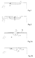
- an avalanche diode is formed by forming in a substrate 1 of a first conductivity type, a region 2 of the opposite conductivity type.
- substrate is used here to designate a region or upper layer of a semiconductor component, for example an integrated circuit.
- the region 2 is generally highly doped and the breakdown threshold of the avalanche diode is essentially determined by the doping level of the substrate 1 (the less the substrate is doped, the greater the breakdown voltage of the device is high).
- Figure 2 shows another example of an avalanche diode commonly used in integrated circuits.
- a diffused (or implanted-diffused) region 3 of the same first type of conductivity is produced in the substrate 1 of the first conductivity type.
- a region 2 of the opposite conductivity type is formed so as to protrude laterally with respect to the region 3 to obtain an independent breakdown of edge and surface effects.
- the avalanche voltage of the junction 2-3 which depends on the doping level of the P region is necessarily lower than that of junction 2-1 since the concentration of region 3 at its junction with region 2 is necessarily greater than that of region 1.
- any method of manufacturing a semiconductor component or an integrated circuit one can use the various types of diffusion provided for the manufacture of other components of the integrated circuit to form avalanche diodes.
- the breakdown thresholds of the various diodes are determined without possibility of choice by the doping level of the existing regions, and in many simple integrated circuit manufacturing processes such as integrated power circuits, only the two possibilities illustrated in Figures 1 and 2.
- an object of the present invention is to provide a method for manufacturing a determined threshold avalanche diode, distinct from the naturally occurring thresholds by using the existing junctions in a given sector, this threshold being able to be chosen without adding a step additional processing at existing steps.
- the present invention provides a method of manufacturing a threshold avalanche diode determined in a substrate of a first type of low doping conductivity, comprising the steps of diffusing into the substrate at least a first region of the first conductivity type; diffusing into the substrate a second region of the second type of conductivity overflowing with respect to the first region.
- the opening of a definition mask of the first region has a lateral extent less than the diffusion depth of the first region in the substrate, this lateral extent being chosen all the more low as the avalanche threshold sought is high. .
- each diffusion is preceded by an implantation.
- each first region comprises a plurality of disjoint and identical subregions.
- the present invention also provides a method for the simultaneous manufacture of several avalanche diodes of distinct and determined thresholds in a substrate of a first type of low doping conductivity comprising the steps of diffusing into the substrate first regions of the first conductivity type; diffusing into the substrate second regions of the second type of conductivity each of which overflows with respect to a first region.
- the openings of the definition masks of each of the first regions have distinct lateral extents, less than the diffusion depth of the first regions, the lateral extent being even smaller than the required avalanche threshold is high.
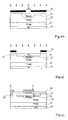
- Figure 3A shows a first step of manufacturing an avalanche diode according to the present invention.
- the structure is formed in a substrate 1 of a first type of conductivity which will be considered hereinafter by way of example as type P.
- a substrate 1 of a first type of conductivity which will be considered hereinafter by way of example as type P.
- an implantation mask 10 having an opening 11.
- a dopant of type P is implanted in this substrate and then made to diffuse to form a P-type region 12 more strongly doped than the substrate.
- the opening in the mask 11 is chosen smaller than the diffusion depth of the region 12.
- an N-type region 13 heavily doped with an overflow with respect to the region 12 is implanted and diffused.
- the diffusion of dopant from the implanted area is also important that laterally in the direction of depth.
- this region is more lightly doped than in the case of the layer 3 in Figure 2 which has a substantially greater width its depth. It will be understood that the doping at the interface is even lower than the opening 11 is smaller.
- An avalanche diode is thus obtained between the regions 13 and 12 of avalanche voltage intermediate between those of the diodes. avalanche of Figures 1 and 3.
- this avalanche diode has an adjustable threshold which depends on the size of the opening 11 in the mask 10. It will simultaneously be formed in the substrate 1 several avalanche diodes each having the threshold corresponding to that of Figure 1, the others having the threshold corresponding to the structure of Figure 2, and still others, according to the invention, having chosen thresholds intermediate between those of the structures of Figures 1 and 2.
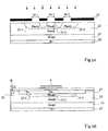
- FIGS. 4A-4C An embodiment of the present invention will be described in more detail with reference to FIGS. 4A-4C in the context of a technology for manufacturing power MOS transistors associated with logic circuits, in which the structure is formed on a strongly doped N-type silicon wafer 20 on which is formed an N type epitaxial layer 21.
- a P type box 22 which, in the context of manufacturing power MOS transistors associated with circuits logical, corresponds to the diffusion in which are formed the boxes of the logic circuits. It is this box diffusion which corresponds to the "substrate" 1 of FIGS. 1 to 3.
- a P-type dopant such as boron
- this step doping corresponding for example to the formation of boxes of type DMOS transistors in the power portion of the circuit.
- a diffused region similar to region 12 of FIG. 3A is obtained.
- a mask 26 is used to form a heavily doped N-type layer 27 which corresponds, for example, to the source regions of the DMOS transistors.
- an insulating oxide 28 is deposited, a heavily-doped P-type region 29 is formed for resuming contact on the region 22, and then cathode metallizations K are formed and on the region 29 and anode A on region 27.
- junction between the region 27 and the region 22 would have in a particular manufacturing process a voltage 20 V and that the junction between the N + region and an extended region would have a breakdown voltage of the order of 7 volts, it is possible to obtain, depending on the value of the opening 24, a breakdown voltage diode. chosen between these two values.
- Figs. 5A, 5B illustrate an alternative embodiment of the present invention shown in the context of the embodiment of Figs. 4A-4C.
- a plurality of apertures 24-1, 24-2, 24-3 are formed therein to form a plurality of regions 25-1, 25-2, 25-3 identical to each other. other but overlapping because of the choice of a small gap between the openings. It is then possible to obtain, as shown in FIG. 5B, a diode with a threshold avalanche chosen but of greater surface area to allow larger currents to pass.
- P + -N type avalanche diodes For example by diffusion in the epitaxial layer 21, at a location where it is apparent on the surface of the substrate.
- a P + diffusion in the epitaxial layer form a diode to a avalanche voltage of about 35 volts
Description
La présente invention concerne la fabrication de diodes à avalanche dans des circuits intégrés, par exemple des circuits intégrés de puissance.The present invention relates to the manufacture of avalanche diodes in integrated circuits, for example integrated power circuits.
Dans de tels circuits, on a souvent besoin de définir plusieurs seuils de déclenchement, par exemple pour réaliser divers dispositifs de protection contre des décharges électrostatiques, des inversions de batterie, et autres.In such circuits, it is often necessary to define several trip thresholds, for example to achieve various protection devices against electrostatic discharges, battery inversions, and the like.
De façon générale, comme le représente la figure 1, une diode à avalanche est réalisée en formant dans un substrat 1 d'un premier type de conductivité, une région 2 du type de conductivité opposé. On notera que le terme substrat est utilisé ici pour désigner une région ou couche supérieure d'un composant semiconducteur, par exemple un circuit intégré. La région 2 est généralement fortement dopée et le seuil de claquage de la diode à avalanche est essentiellement déterminé par le niveau de dopage du substrat 1 (moins le substrat est dopé, plus la tension de claquage du dispositif est élevée).In general, as shown in Figure 1, an avalanche diode is formed by forming in a
La figure 2 représente un autre exemple de diode à avalanche couramment utilisé dans des circuits intégrés. Dans le substrat 1 du premier type de conductivité, est réalisée une région 3 diffusée (ou implantée-diffusée) du même premier type de conductivité. Une région 2 du type de conductivité opposé est formée de façon à déborder latéralement par rapport à la région 3 pour obtenir un claquage indépendant des effets de bord et de surface. En supposant que le substrat 1 de la figure 2 est le même que celui de la figure 1, la tension d'avalanche de la jonction 2-3, qui dépend du niveau de dopage de la région P, est nécessairement moins élevée que celle de la jonction 2-1 puisque la concentration de la région 3 à sa jonction avec la région 2 est nécessairement plus élevée que celle de la région 1.Figure 2 shows another example of an avalanche diode commonly used in integrated circuits. In the
Ainsi, de façon générale, dans tout procédé de fabrication d'un composant semiconducteur ou d'un circuit intégré, on peut utiliser les divers types de diffusion prévus pour la fabrication d'autres composants du circuit intégré pour former des diodes à avalanche. Toutefois, les seuils de claquage des diverses diodes sont déterminés sans possibilité de choix par le niveau de dopage des régions existantes et, dans de nombreuses filières simples de fabrication de circuits intégrés tels que des circuits intégrés de puissance, il n'existe que les deux possibilités illustrées en figures 1 et 2.Thus, in general, in any method of manufacturing a semiconductor component or an integrated circuit, one can use the various types of diffusion provided for the manufacture of other components of the integrated circuit to form avalanche diodes. However, the breakdown thresholds of the various diodes are determined without possibility of choice by the doping level of the existing regions, and in many simple integrated circuit manufacturing processes such as integrated power circuits, only the two possibilities illustrated in Figures 1 and 2.
Ainsi, dans un dispositif existant, pour obtenir une diode à seuil d'avalanche spécifique, il faudrait prévoir une région diffusée 3 spécifique, c'est-à-dire à dose d'implantation spécifique ou à durée de recuit spécifique. Il est bien entendu inimaginable dans un circuit intégré de prévoir une zone à durée de recuit spécifique car le recuit réalisé pour cette zone réagirait sur les autres zones du circuit intégré. D'autre part, réaliser une implantation à dose spécifique augmenterait le nombre d'étapes de fabrication du circuit intégré, ce que l'on cherche toujours à éviter dans une filière existante. Une structure de diode selon la préambule de la revendication 1 est connue de JP-A-59-079 578 et de EP-A-359 679.Thus, in an existing device, to obtain a specific avalanche threshold diode, it would be necessary to provide a specific scattered
Ainsi, un objet de la présente invention est de prévoir un procédé de fabrication d'une diode à avalanche de seuil déterminé, distinct des seuils existant naturellement en utilisant les jonctions existantes dans une filière déterminée, ce seuil pouvant être choisi sans ajouter d'étape de traitement supplémentaire aux étapes existantes.Thus, an object of the present invention is to provide a method for manufacturing a determined threshold avalanche diode, distinct from the naturally occurring thresholds by using the existing junctions in a given sector, this threshold being able to be chosen without adding a step additional processing at existing steps.
Pour atteindre ces objets, la présente invention prévoit un procédé de fabrication d'une diode à avalanche à seuil déterminé dans un substrat d'un premier type de conductivité à faible niveau de dopage, comprenant les étapes consistant à faire diffuser dans le substrat au moins une première région du premier type de conductivité ; faire diffuser dans le substrat une deuxième région du deuxième type de conductivité débordant par rapport à la première région. L'ouverture d'un masque de définition de la première région a une étendue latérale inférieure à la profondeur de diffusion de la première région dans le substrat, cette étendue latérale étant choisie d'autant plus faible que le seuil d'avalanche recherché est élevé.To achieve these objects, the present invention provides a method of manufacturing a threshold avalanche diode determined in a substrate of a first type of low doping conductivity, comprising the steps of diffusing into the substrate at least a first region of the first conductivity type; diffusing into the substrate a second region of the second type of conductivity overflowing with respect to the first region. The opening of a definition mask of the first region has a lateral extent less than the diffusion depth of the first region in the substrate, this lateral extent being chosen all the more low as the avalanche threshold sought is high. .
Selon un mode de réalisation de la présente invention, chaque diffusion est précédée d'une implantation.According to one embodiment of the present invention, each diffusion is preceded by an implantation.
Selon un mode de réalisation de la présente invention, chaque première région comprend une pluralité de sous-régions disjointes et identiques.According to an embodiment of the present invention, each first region comprises a plurality of disjoint and identical subregions.
La présente invention prévoit aussi un procédé de fabrication simultanée de plusieurs diodes à avalanche de seuils distincts et déterminés dans un substrat d'un premier type de conductivité à faible niveau de dopage comprenant les étapes consistant à faire diffuser dans le substrat des premières régions du premier type de conductivité ; faire diffuser dans le substrat des deuxièmes régions du deuxième type de conductivité dont chacune déborde par rapport à une première région. Les ouvertures des masques de définition de chacune des premières régions ont des étendues latérales distinctes, inférieures à la profondeur de diffusion des premières régions, l'étendue latérale étant d'autant plus faible que le seuil d'avalanche recherché est élevé.The present invention also provides a method for the simultaneous manufacture of several avalanche diodes of distinct and determined thresholds in a substrate of a first type of low doping conductivity comprising the steps of diffusing into the substrate first regions of the first conductivity type; diffusing into the substrate second regions of the second type of conductivity each of which overflows with respect to a first region. The openings of the definition masks of each of the first regions have distinct lateral extents, less than the diffusion depth of the first regions, the lateral extent being even smaller than the required avalanche threshold is high.
Ces objets, caractéristiques et avantages, ainsi que d'autres de la présente invention seront exposés en détail dans la description suivante de modes de réalisation particuliers faite à titre non-limitatif en relation avec les figures jointes parmi lesquelles :
- les figures 1 et 2 représentent des diodes à avalanche selon l'art antérieur ;
- les figures 3A et 3B illustrent des étapes de réalisation d'une diode à avalanche selon la présente invention ;
- les figures 4A à 4C illustrent des étapes de réalisation d'une diode à avalanche selon la présente invention ; et
- les figures 5A et 5B illustrent des étapes de réalisation d'une diode à avalanche selon la présente invention.
- Figures 1 and 2 show avalanche diodes according to the prior art;
- FIGS. 3A and 3B illustrate steps of making an avalanche diode according to the present invention;
- FIGS. 4A to 4C illustrate steps of making an avalanche diode according to the present invention; and
- FIGS. 5A and 5B illustrate steps for producing an avalanche diode according to the present invention.
La figure 3A représente une première étape de fabrication d'une diode à avalanche selon la présente invention. La structure est formée dans un substrat 1 d'un premier type de conductivité qui sera considéré ci-après à titre d'exemple comme le type P. Sur ce substrat est formé un masque d'implantation 10 comportant une ouverture 11. Un dopant de type P est implanté dans ce substrat puis amené à diffuser pour former une région 12 de type P plus fortement dopée que le substrat. L'ouverture dans le masque 11 est choisie inférieure à la profondeur de diffusion de la région 12.Figure 3A shows a first step of manufacturing an avalanche diode according to the present invention. The structure is formed in a
A une étape suivante, on implante et on fait diffuser une région 13 de type N fortement dopée en débordement par rapport à la région 12.In a next step, an N-
Etant donné que la dimension latérale de l'ouverture 11 dans le masque 10 est inférieure à la profondeur de diffusion de la région P, la diffusion des dopants à partir de la zone implantée est aussi importante latéralement que dans le sens de la profondeur. Ainsi, au niveau de la partie profonde de la région 12 et plus particulièrement au niveau de son interface avec la région 13, cette région se trouve plus faiblement dopée que dans le cas de la couche 3 de la figure 2 qui a une largeur nettement supérieure à sa profondeur. On comprendra que le dopage à l'interface est d'autant plus faible que l'ouverture 11 est plus petite. On dispose ainsi d'un moyen pour régler le niveau de dopage de la région 12 au niveau de sa jonction avec la région 13. On obtient ainsi une diode à avalanche entre les régions 13 et 12 de tension d'avalanche intermédiaire entre celles des diodes à avalanche des figures 1 et 3. De plus, cette diode à avalanche a un seuil réglable qui dépend de la dimension de l'ouverture 11 dans le masque 10. On pourra former simultanément dans le substrat 1 plusieurs diodes à avalanche les unes ayant le seuil correspondant à celui de la figure 1, les autres ayant le seuil correspondant à la structure de la figure 2, et d'autres encore, selon l'invention, ayant des seuils choisis intermédiaires entre ceux des structures des figures 1 et 2.Since the lateral dimension of the
On va décrire plus en détail un mode de réalisation de la présente invention en relation avec les figures 4A à 4C dans le cadre d'une technologie de fabrication de transistors MOS de puissance associés à des circuits logiques, dans laquelle la structure est formée sur une tranche de silicium de type N fortement dopée 20 sur laquelle est formée une couche épitaxiée 21 de type N. Dans cette couche épitaxiée est formé un caisson 22 de type P qui, dans le cadre de la fabrication de transistors MOS de puissance associés à des circuits logiques, correspond à la diffusion dans laquelle sont formés les caissons des circuits logiques. C'est cette diffusion de caisson qui correspond au "substrat" 1 des figures 1 à 3. Dans ce caisson, à travers un masque 23 présentant une ouverture de dimension réduite 24 est implanté un dopant de type P tel que du bore, cette étape de dopage correspondant par exemple à la formation de caissons de transistors de type DMOS dans la partie de puissance du circuit. Après recuit, on obtient une région diffusée 25 analogue à la région 12 de la figure 3A. Alors, comme le représente la figure 4B, on procède à travers un masque 26 à la formation d'une couche de type N fortement dopée 27 qui correspond par exemple aux régions de source de transistors DMOS. Enfin, comme le représente la figure 4C, on dépose un oxyde d'isolement 28, on forme une région 29 de type P fortement dopée de reprise de contact sur la région 22, puis l'on forme des métallisations de cathode K et sur la région 29 et d'anode A sur la région 27.An embodiment of the present invention will be described in more detail with reference to FIGS. 4A-4C in the context of a technology for manufacturing power MOS transistors associated with logic circuits, in which the structure is formed on a strongly doped N-
Tandis que la jonction entre la région 27 et la région 22 aurait dans un procédé de fabrication particulier une tension de claquage de 20 volts et que la jonction entre la région N+ et une région 25 étendue aurait une tension de claquage de l'ordre de 7 volts, on peut obtenir, selon la valeur de l'ouverture 24 une diode de tension de claquage choisie entre ces deux valeurs.While the junction between the
Les figures 5A, 5B illustrent une variante de réalisation de la présente invention représentée dans le cadre du mode de réalisation des figures 4A-4C.Figs. 5A, 5B illustrate an alternative embodiment of the present invention shown in the context of the embodiment of Figs. 4A-4C.
Au lieu de former dans le masque 23 une ouverture 24 unique, on y forme plusieurs ouvertures 24-1, 24-2, 24-3 de façon à former plusieurs régions 25-1, 25-2, 25-3 identiques les unes aux autres mais se recoupant en raison du choix d'un faible espacement entre les ouvertures. On peut alors obtenir comme le représente la figure 5B une diode à avalanche de seuil choisi mais de plus grande surface pour permettre de laisser passer des courants plus importants.Instead of forming a
Bien que la présente invention ait été décrite dans le cadre de modes de réalisation particuliers, elle s'applique également à la formation de diodes à avalanche de type P+-N. Par exemple par diffusion dans la couche épitaxiée 21, à un emplacement où elle est apparente en surface du substrat. Dans le cas particulier où une diffusion P+ dans cette couche épitaxiée formerait une diode d'une tension d'avalanche de l'ordre de 35 volts, on peut réaliser des diodes à avalanche de toute valeur supérieure à 35 volts, en diffusant une ou plusieurs régions de type N à travers un masque à ouvertures étroites puis en formant une couche d'anode de type P+.Although the present invention has been described in the context of particular embodiments, it also applies to the formation of P + -N type avalanche diodes. For example by diffusion in the
Claims (4)
- A method of manufacturing an avalanche diode of determined threshold in a substrate (1; 22) of a first conductivity type with a low doping level, including the steps of:diffusing in the substrate at least one first region (12; 25) of the first conductivity type;diffusing in the substrate a second region (13; 27) of the second conductivity type protruding from the first region;characterized in that the opening (11; 24) of a mask (10; 23) of definition of the first region (12; 25) has a lateral extent smaller than the diffusion depth of the first region in the substrate, this lateral extent being chosen all the smaller as the desired avalanche threshold is high.
- The method of claim 1, characterized in that each diffusion is preceded by an implantation.
- The method of claim 1, characterized in that each first region includes a plurality of separate and identical sub-regions (25-1, 25-2, 25-3).
- A method of simultaneously manufacturing several avalanche diodes of distinct and determined thresholds in a substrate (22) of a first conductivity type of low doping level including the steps of:diffusing in the substrate first regions (25-1, 25-2, 25-3) of the first conductivity type;diffusing in the substrate second regions (27) of the second conductivity type, each of which protrudes from a first region;characterized in that the openings (24-1, 24-2, 24-3) of the masks of definition of each of the first regions have lateral extents smaller than the diffusion depths of the first regions, the lateral extent being all the smaller as the desired avalanche threshold is high.
Applications Claiming Priority (2)
| Application Number | Priority Date | Filing Date | Title |
|---|---|---|---|
| FR9804207 | 1998-03-31 | ||
| FR9804207A FR2776827B1 (en) | 1998-03-31 | 1998-03-31 | METHOD FOR MANUFACTURING AN AVALANCHE DIODE WITH ADJUSTABLE THRESHOLD |
Publications (2)
| Publication Number | Publication Date |
|---|---|
| EP0948038A1 EP0948038A1 (en) | 1999-10-06 |
| EP0948038B1 true EP0948038B1 (en) | 2007-01-24 |
Family
ID=9524865
Family Applications (1)
| Application Number | Title | Priority Date | Filing Date |
|---|---|---|---|
| EP99410025A Expired - Lifetime EP0948038B1 (en) | 1998-03-31 | 1999-03-30 | Method of fabricating an avalanche diode with controllable threshold |
Country Status (4)
| Country | Link |
|---|---|
| US (1) | US6306717B1 (en) |
| EP (1) | EP0948038B1 (en) |
| DE (1) | DE69934928D1 (en) |
| FR (1) | FR2776827B1 (en) |
Families Citing this family (2)
| Publication number | Priority date | Publication date | Assignee | Title |
|---|---|---|---|---|
| EP1191598B1 (en) * | 2000-01-18 | 2007-12-19 | Siemens Schweiz AG | Method for fabricating a semiconductor photosensor |
| US8087415B2 (en) * | 2009-02-24 | 2012-01-03 | Zen Design Solutions Limited | Adjustable applicator assembly |
Family Cites Families (5)
| Publication number | Priority date | Publication date | Assignee | Title |
|---|---|---|---|---|
| US4064620A (en) * | 1976-01-27 | 1977-12-27 | Hughes Aircraft Company | Ion implantation process for fabricating high frequency avalanche devices |
| JPS57122579A (en) * | 1981-01-22 | 1982-07-30 | Mitsubishi Electric Corp | Zener diode |
| US4416708A (en) * | 1982-01-15 | 1983-11-22 | International Rectifier Corporation | Method of manufacture of high speed, high power bipolar transistor |
| JPS5979578A (en) * | 1982-10-29 | 1984-05-08 | Hitachi Ltd | Low voltage zener diode and manufacture thereof |
| FR2636474B1 (en) | 1988-09-09 | 1990-11-30 | Sgs Thomson Microelectronics | METHOD FOR MANUFACTURING A REGULATION AND PROTECTION DIODE |
-
1998
- 1998-03-31 FR FR9804207A patent/FR2776827B1/en not_active Expired - Fee Related
-
1999
- 1999-03-30 EP EP99410025A patent/EP0948038B1/en not_active Expired - Lifetime
- 1999-03-30 US US09/282,025 patent/US6306717B1/en not_active Expired - Lifetime
- 1999-03-30 DE DE69934928T patent/DE69934928D1/en not_active Expired - Lifetime
Also Published As
| Publication number | Publication date |
|---|---|
| FR2776827B1 (en) | 2000-06-16 |
| EP0948038A1 (en) | 1999-10-06 |
| US6306717B1 (en) | 2001-10-23 |
| DE69934928D1 (en) | 2007-03-15 |
| FR2776827A1 (en) | 1999-10-01 |
Similar Documents
| Publication | Publication Date | Title |
|---|---|---|
| FR2530867A1 (en) | MOS DEVICES WITH SCHOTTKY BARRIER AND METHOD OF MANUFACTURING SAME | |
| FR2569495A1 (en) | METHOD FOR MANUFACTURING SEMICONDUCTOR DEVICES HAVING VARIABLE LOAD CONCENTRATION PLANAR JUNCTIONS WITH VERY HIGH BREAKAGE VOLTAGE | |
| EP0420748A1 (en) | Process of fabricating a high-tension MIS integrated circuit | |
| EP0013340A1 (en) | Resistance with improved breakdown characteristics, made by a double ion implantation process in a semi-conductor substrate, and method of making it | |
| EP0581625B1 (en) | Multifunctional electronic device, in particular element with a negative dynamic resistance and corresponding method of fabrication | |
| FR2739976A1 (en) | TERMINATION STRUCTURE, SEMICONDUCTOR DEVICE, AND METHODS OF MAKING THE SAME | |
| FR2735904A1 (en) | METHOD OF MAKING A SEMICONDUCTOR WITH A HIGHLY DOPED ZONE BETWEEN LOWLY DOPED AREAS, FOR THE MANUFACTURE OF TRANSISTORS | |
| EP0624943B1 (en) | Serial current limiting device | |
| FR2953062A1 (en) | LOW VOLTAGE BIDIRECTIONAL PROTECTION DIODE | |
| FR2606214A1 (en) | BIPOLAR HETEROJUNCTION TRANSISTOR | |
| FR3067516A1 (en) | IMPLEMENTING SEMICONDUCTOR REGIONS IN AN ELECTRONIC CHIP | |
| EP0948038B1 (en) | Method of fabricating an avalanche diode with controllable threshold | |
| FR2482368A1 (en) | LOGIC OPERATOR WITH INJECTION BY THE SUBSTRATE AND METHOD OF MANUFACTURING THE SAME | |
| EP1111684A1 (en) | Process for making vertical power components | |
| EP1006573B1 (en) | Method for manufacturing integrated BiCMOS circuits on a common CMOS substrate | |
| EP1146561A1 (en) | Method of manufacturing a bipolar transistor | |
| EP0462029B1 (en) | Process of fabricating a bipolar transistor sustaining a reverse bias | |
| EP0881672A1 (en) | Isolation wall between power device | |
| EP0037764B1 (en) | Unipolar functioning semiconductor device structure with guard ring | |
| EP0607075B1 (en) | Semiconductor electronic component having a negative dynamic resistance and corresponding using methods and manufacturing process | |
| EP0065464B1 (en) | Process for manufacturing mos-type integrated circuits | |
| FR2826779A1 (en) | ANTISTATIC CONTACT FOR POLYCRYSTALLINE SILICON LINE | |
| WO1998047173A1 (en) | Mos transistor with high doping gradient under the grid | |
| EP1146554A1 (en) | Method for forming buried layers | |
| EP0872893A1 (en) | PNP lateral transistor in CMOS technology |
Legal Events
| Date | Code | Title | Description |
|---|---|---|---|
| PUAI | Public reference made under article 153(3) epc to a published international application that has entered the european phase |
Free format text: ORIGINAL CODE: 0009012 |
|
| AK | Designated contracting states |
Kind code of ref document: A1 Designated state(s): DE FR GB IT |
|
| AX | Request for extension of the european patent |
Free format text: AL;LT;LV;MK;RO;SI |
|
| 17P | Request for examination filed |
Effective date: 20000316 |
|
| AKX | Designation fees paid |
Free format text: DE FR GB IT |
|
| RAP1 | Party data changed (applicant data changed or rights of an application transferred) |
Owner name: STMICROELECTRONICS S.A. |
|
| GRAP | Despatch of communication of intention to grant a patent |
Free format text: ORIGINAL CODE: EPIDOSNIGR1 |
|
| GRAS | Grant fee paid |
Free format text: ORIGINAL CODE: EPIDOSNIGR3 |
|
| GRAA | (expected) grant |
Free format text: ORIGINAL CODE: 0009210 |
|
| AK | Designated contracting states |
Kind code of ref document: B1 Designated state(s): DE FR GB IT |
|
| REG | Reference to a national code |
Ref country code: GB Ref legal event code: FG4D Free format text: NOT ENGLISH |
|
| REF | Corresponds to: |
Ref document number: 69934928 Country of ref document: DE Date of ref document: 20070315 Kind code of ref document: P |
|
| PG25 | Lapsed in a contracting state [announced via postgrant information from national office to epo] |
Ref country code: DE Free format text: LAPSE BECAUSE OF FAILURE TO SUBMIT A TRANSLATION OF THE DESCRIPTION OR TO PAY THE FEE WITHIN THE PRESCRIBED TIME-LIMIT Effective date: 20070425 |
|
| GBT | Gb: translation of ep patent filed (gb section 77(6)(a)/1977) |
Effective date: 20070425 |
|
| PLBE | No opposition filed within time limit |
Free format text: ORIGINAL CODE: 0009261 |
|
| STAA | Information on the status of an ep patent application or granted ep patent |
Free format text: STATUS: NO OPPOSITION FILED WITHIN TIME LIMIT |
|
| 26N | No opposition filed |
Effective date: 20071025 |
|
| PG25 | Lapsed in a contracting state [announced via postgrant information from national office to epo] |
Ref country code: IT Free format text: LAPSE BECAUSE OF FAILURE TO SUBMIT A TRANSLATION OF THE DESCRIPTION OR TO PAY THE FEE WITHIN THE PRESCRIBED TIME-LIMIT Effective date: 20070124 |
|
| PGFP | Annual fee paid to national office [announced via postgrant information from national office to epo] |
Ref country code: GB Payment date: 20080225 Year of fee payment: 10 |
|
| PGFP | Annual fee paid to national office [announced via postgrant information from national office to epo] |
Ref country code: FR Payment date: 20080530 Year of fee payment: 10 |
|
| GBPC | Gb: european patent ceased through non-payment of renewal fee |
Effective date: 20090330 |
|
| REG | Reference to a national code |
Ref country code: FR Ref legal event code: ST Effective date: 20091130 |
|
| PG25 | Lapsed in a contracting state [announced via postgrant information from national office to epo] |
Ref country code: GB Free format text: LAPSE BECAUSE OF NON-PAYMENT OF DUE FEES Effective date: 20090330 Ref country code: FR Free format text: LAPSE BECAUSE OF NON-PAYMENT OF DUE FEES Effective date: 20091123 |