EP0947979A2 - Tone signal generator having a sound effect function - Google Patents
Tone signal generator having a sound effect function Download PDFInfo
- Publication number
- EP0947979A2 EP0947979A2 EP99111094A EP99111094A EP0947979A2 EP 0947979 A2 EP0947979 A2 EP 0947979A2 EP 99111094 A EP99111094 A EP 99111094A EP 99111094 A EP99111094 A EP 99111094A EP 0947979 A2 EP0947979 A2 EP 0947979A2
- Authority
- EP
- European Patent Office
- Prior art keywords
- data
- tone signal
- phase
- tone
- circuit
- Prior art date
- Legal status (The legal status is an assumption and is not a legal conclusion. Google has not performed a legal analysis and makes no representation as to the accuracy of the status listed.)
- Granted
Links
Images


Classifications
-
- G—PHYSICS
- G10—MUSICAL INSTRUMENTS; ACOUSTICS
- G10K—SOUND-PRODUCING DEVICES; METHODS OR DEVICES FOR PROTECTING AGAINST, OR FOR DAMPING, NOISE OR OTHER ACOUSTIC WAVES IN GENERAL; ACOUSTICS NOT OTHERWISE PROVIDED FOR
- G10K15/00—Acoustics not otherwise provided for
- G10K15/02—Synthesis of acoustic waves
-
- G—PHYSICS
- G10—MUSICAL INSTRUMENTS; ACOUSTICS
- G10H—ELECTROPHONIC MUSICAL INSTRUMENTS; INSTRUMENTS IN WHICH THE TONES ARE GENERATED BY ELECTROMECHANICAL MEANS OR ELECTRONIC GENERATORS, OR IN WHICH THE TONES ARE SYNTHESISED FROM A DATA STORE
- G10H7/00—Instruments in which the tones are synthesised from a data store, e.g. computer organs
- G10H7/002—Instruments in which the tones are synthesised from a data store, e.g. computer organs using a common processing for different operations or calculations, and a set of microinstructions (programme) to control the sequence thereof
- G10H7/004—Instruments in which the tones are synthesised from a data store, e.g. computer organs using a common processing for different operations or calculations, and a set of microinstructions (programme) to control the sequence thereof with one or more auxiliary processor in addition to the main processing unit
-
- G—PHYSICS
- G10—MUSICAL INSTRUMENTS; ACOUSTICS
- G10H—ELECTROPHONIC MUSICAL INSTRUMENTS; INSTRUMENTS IN WHICH THE TONES ARE GENERATED BY ELECTROMECHANICAL MEANS OR ELECTRONIC GENERATORS, OR IN WHICH THE TONES ARE SYNTHESISED FROM A DATA STORE
- G10H1/00—Details of electrophonic musical instruments
- G10H1/02—Means for controlling the tone frequencies, e.g. attack or decay; Means for producing special musical effects, e.g. vibratos or glissandos
- G10H1/04—Means for controlling the tone frequencies, e.g. attack or decay; Means for producing special musical effects, e.g. vibratos or glissandos by additional modulation
- G10H1/053—Means for controlling the tone frequencies, e.g. attack or decay; Means for producing special musical effects, e.g. vibratos or glissandos by additional modulation during execution only
- G10H1/057—Means for controlling the tone frequencies, e.g. attack or decay; Means for producing special musical effects, e.g. vibratos or glissandos by additional modulation during execution only by envelope-forming circuits
- G10H1/0575—Means for controlling the tone frequencies, e.g. attack or decay; Means for producing special musical effects, e.g. vibratos or glissandos by additional modulation during execution only by envelope-forming circuits using a data store from which the envelope is synthesized
-
- G—PHYSICS
- G10—MUSICAL INSTRUMENTS; ACOUSTICS
- G10H—ELECTROPHONIC MUSICAL INSTRUMENTS; INSTRUMENTS IN WHICH THE TONES ARE GENERATED BY ELECTROMECHANICAL MEANS OR ELECTRONIC GENERATORS, OR IN WHICH THE TONES ARE SYNTHESISED FROM A DATA STORE
- G10H1/00—Details of electrophonic musical instruments
- G10H1/18—Selecting circuits
- G10H1/183—Channel-assigning means for polyphonic instruments
Definitions
- the present invention relates to a tone signal generator which can generate tone signals to which various specialized sound effects such as modulation and pitch change are provided, along with musical tones and normal sound effects, and particularly to improvement in access efficiency to a memory in which the tone signals are stored.
- tone signal generators TV game and electronic musical instruments for entertainment in practical use have tone signal generators.
- data of tone signals stored in a game cartridge provided by a ROM or a CD - ROM is supplied into an internal RAM of the game instrument, and the data is read according to progress of a game program carried out for generating, musical tones with the normal sound effects and the musical tones as background music.
- filter data for imparting various sound effects to tone signal data to be generated in the RAM along with the above described data, and a buffer area for imparting the sound effects and other areas for storing process data are also assigned in the RAM.
- a CPU and other devices in the TV game or musical instrument frequently access the RAM.
- the RAM is accessed continuously till a keyoff signal (i.e., a note off signal) is inputted, even though the tone signal in generating becomes the lowest level that no sound is to be substantially heard.
- a keyoff signal i.e., a note off signal
- US 4,357,849 discloses a key switch information assignor. When a key is depressed or released a keyboard circuit produces respective key information. A data processor then determines whether a these information correspond to either a depression or release of a key and generates a key code combining all key information. This key code is then sent to an assignment memory. An envelope generator determines the end of note sounding, releases the corresponding key code from the assignment memory at the same time, and sends this information back to the data processor. In case all channels of the assignment memory are in use the CPU generates a demand signal interrupting the processing under execution allowing the channels of the assignment memory to be quickly released.
- an electronic musical instrument comprising a keyboard.
- a CPU assigns key codes to selected tone generating channels of a RAM. Thereby a tone is generated according to the assigned key code.
- each of the key codes stored in the RAM is fed to an envelope generator to generate data representing the amplitude of the envelopes of the corresponding tone.
- the CPU modifies these data by using weighting data corresponding to the respective key codes supplied by a ROM. Based on these weighting data the CPU selects the "least important" one replacing it by the data corresponding to the newly depressed key of the keyboard.
- the tone signal generator usually is provided with a generator for generating envelope wave data which is imparted to the tone signal data read from the RAM.
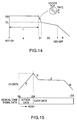
- Fig. 15 shows an example of the tone signal data, for example, musical tone signal data, and the envelope wave data (EG data).
- the tone signal data includes attack data arranged in an attack part of the tone signal data, and loop data arranged in the following part.
- the EG data is divided, as shown in Fig. 15, into four phases, A- attack phase, D- decay phase, S-. sustain phase (or D2. second decay phase), and, R- release phase.
- the loop data is arranged between a loop start address LSA and a loop end address LEA, and when the read address reaches the LEA, the read address returns to the LSA, thereby the read address being looped between the LSA and the LEA.
- a read address changing width of the tone signal data is changed. That is, if the pitch is changed high, the read address changing width is changed large, and if the pitch is changed low, the read address changing width is changed small.
- a prior tone signal generator is provided with a key scaling way in which a gradient of the attack phase is changed in response to the pitch changing.
- the key scaling way it is difficult to keep severe phrase matching between the attack phase in the EG data and the attack data in the tone signal data, and to simplify a structure for changing a shape of the EG data.
- an embodiment of it comprises a memory for storing tone signal data, the tone signal data including attack data for an attack phase of the tone signal data and following data for a following phase of the tone signal data; a read controller for reading the tone signal data from the memory; an envelope data generator for generating envelope data corresponding to the attack phase and the following phase of the tone single data; and an envelope imparting circuit for modifying the tone signal data read by the read controller based on the envelope data generated by the envelope data generator, wherein when the read controller ends reading of the attack phase of the tone signal data, a phase of the envelope data generated by the envelope data generator is changed from the attack phase to the following phase in order to match a phase timing of the envelope data and the tone signal data.
- the read controller generates a control signal when it ends reading of the attack phase of the tone signal data, and a phase change controller changes the phase of the envelope data generated by the envelope data generator from the attack phase to the following phase when the control signal is generated by the read controller.
- the tone signal generator may be set up such that the envelope data generator selects a data change rate, before the control signal is generated by the read controller, the envelope data generator selects a first data change rate, and when the control signal is generated by the read controller, the phase change controller changes the phase of the envelope data from the attack phase to the following phase by causing the envelope data generator to select a second data change rate, which is different from the first data change rate.
- This configuration of a tone signal generator allows the phase timing of the envelope data and the tone signal data to be severely matched.
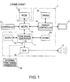
- Fig. 1 is a block diagram of a TV game instrument, to which a tone signal generator LSI is applied, embodying the present invention.
- a display 4 and a speaker 5 are connected to a game instrument 1.
- the display 4 and the speaker 5 can be used as ones installed into a normal TV receiver.
- a game cartridge 3 having a ROM 19 in which a game program is stored and a controller 2 for a player to play a game are also connected.
- the controller 2 is connected to the game instrument 1 through a cable or the like, and the game cartridge 3 is set into a slot mounted in the game instrument 1.
- the game instrument 1 is equipped with a main CPU (MCPU) 10 which controls a whole program of the game progress.
- MCPU main CPU
- the controller 2 the ROM 19 mounted into the game cartridge 3
- a display controller 14 for controlling the display 4
- a tone signal generator LSI 11 for generating tone signals, such as musical tone signals, with sound effects and musical tones as a back ground music
- a sound CPU (SCPU) 12 a DRAM 13 in which a program for the SCPU 12 and PCM wave data are stored, and a D/A converter 16, for converting generated musical tone data into analogue musical tone signals, are connected to the tone signal generator LSI 11.
- the speaker 5 is connected to the D/A converter 16.
- the tone signal generator LSI 11 is provided with an external input terminal into which digital tone data can be inputted from an external tone signal generator 18.
- a VRAM 15 in which screen display data is stored and the display 4 are connected to the display controller 14.
- the MCPU 10 When the power turns on after the game cartridge 3 is set into the game instrument, the MCPU 10 reads specified screen data and sends it to the display controller 14. Then, the MCPU 10 writes programs and the PCM wave data in the DRAM 13, for generating the tone signal data with the sound effects and the BGM (Back Ground Music) tone signal data. After that, the game program is started by operation of the controller 2, and the re-writing of the screen data and the generating of the tone signal data with the sound effects and the BGM tone signal data are performed. The progress control of the game program, i.e., re-writing of the screen data, is carried out directly by the MCPU 10.
- the MCPU 10 gives instructions to the SCPU 12 for generating the tone signal data with the sound effects and the BGM tone signal data, and the synthesizing of the real tone signal is carried out by the SCPU 12 on the basis of the program and the PCM wave data written into the DRAM 13.
- Fig. 2 is an internal block diagram of the tone signal generator LSI 11.
- a PCM circuit 23 generates digital low frequency signal data, such as the tone signal data and modulation signal data, when it reads the PCM wave data stored in the DRAM 13 (refer to Fig. 1).
- digital low frequency signal data such as the tone signal data and modulation signal data
- the tone signal data with the sound effects and the BGM tone signal data can be individually different in each game program.
- the MCPU 10 and the SCPU 12 are connected through a memory controller 21 and a CPU interface 20, and the PCM circuit 23 and a DSP (digital signal processor) 24 mounted into the tone signal generator LSI 11 are connected through the memory controller 21.
- the MCPU 10, the SCPU 12, the PCM circuit 23 and the DSP 24 are individually accessible to the DRAM 13 by sharing time.
- An internal register 22 is connected to the CPU interface 20. Data set into the PCM circuit 23 and the DSP 24, and data for specifying data to set into them by the MCPU 10 and the SCPU 11 are temporarily stored into the internal register 22.
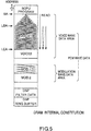
- Fig. 5 shows an internal configuration of the DRAM 13.
- a SCPU program area for the SCPU 12, a PCM wave data area and a DSP ring buffer are assigned.
- the PCM wave data includes voice wave data to generate musical tone signals with the sound effects and the BGM tones, and the modulation wave data used as parameters for the sound effects such as the modulation.
- the plural kinds of voice wave data and the modulation wave data exist and are stored for each data in the DRAM 13.
- the DSP ring buffer area is used to delay the tone signal data to thereby effect the filtering and the modulating or the like in the DSP 24's process.
- the voice wave data sampled data of the tone signals with the sound effects or of natural instrument's tone signals is used generally.
- Such tone signals keep generating tones in long time, so that the voice wave data comprises start address data SA, and the loop start address data LSA and the loop end address data LEA to read repeatedly.
- the SA is read, and then LSA, LEA are read successively and repeatedly.
- the repeated reading between the LSA and the LEA allows generating tone signals to be long time.
- the modulation wave data is generally simple data, such as sin curve wave data or wave data shown in Fig. 7 (Figs. 7A, 7B, 7C), because it is for modulating musical tone signals or the like.
- the SCPU program, the voice wave data and the modulation data are written by the MCPU 10 when the game cartridge 3 is set into the slot.
- the SCPU 12 processes the SCPU program based on the MCPU 10's instructions.
- the PCM circuit 23 reads the PCM wave data based on the SCPU 12's instructions, and generates the digital low frequency signal data.
- the digital low frequency signal data is used as the tone signal data or the sound effect data.
- the PCM circuit 23 has thirty two time sharing channels in which thirty two kinds of the digital low frequency signal data can be generated individually.
- Fig. 9 shows a priority order table of access to the DRAM 13 set in the memory controller 21.
- the process of the tone signal generator LSI 11 is time-shared by thirty two time slots in one sampling clock of the PCM wave data.
- the memory controller 21 is processed by a memory cycle which is generated by division of the sampling clock into one hundred eight. Therefore, four memory cycles are corresponding to one slot in the tone signal generator.
- four priority orders are set as to the memory access right.
- the memory access rights of the DSP 23 and the PCM 24 are assigned alternately, in the second, third and forth priority orders, the memory access rights of a refresh cycle of the DRAM, the MCPU 10, and the SCPU 12 are assigned. Because the DSP 23 and the PCM 24 are required real time processes for the digital low frequency signal data, the highest priority order for them is assigned in the table.
- the PCM circuit 23 generates the digital low frequency signal data by reading the PCM wave data according to instructions of the SCPU 12.
- the digital low frequency signal data is used as the musical tone signal data such as the BGM data or the modulation data.
- the PCM circuit 23 has thirty two time-shared channels, thereby being capable of generating thirty two kinds of the digital low frequency signal data independently.
- the PCM circuit 23 independently monitors a level of the digital low frequency signal data every channel, outputting access inhibit signal data INH to the memory controller 21 by judging that no generation of the digital low frequency signal data is necessary any more, when the level becomes less than a specified value.
- the memory controller 21 stops the access to the DRAM 13 as to the channel, and when any memory access is requested from other device or circuit, the memory controller 21 accesses the DRAM 13 in response to the request, thereby, lower items in the memory access priority table being capable of having a chance to access to the DRAM 13.
- the tone signal data in the digital low frequency signal data that the PCM circuit 23 generates is inputted into the DSP 24 or inputted directly into an out mixing circuit OMIX 25.
- the modulation signal data is inputted into the DSP 24 for coefficients of the sound effects.
- the reading data of the voice wave data area is used as the tone signal data
- the reading data of the modulation wave data area is used as the modulation signal data.
- how to use the signal data is free to thereby generate any desired sound effects.
- the DSP 24 has an outer external terminal into which other tone signal data or other modulation signal data can be inputted.
- the DSP 24 is a circuit for supplying various sound effects, such as modulating, filtering and pitch-changing, to the inputted tone signal data and outputting thus obtained data to the output mixing circuit OMIX 25.
- the modulation signal data which is one of the digital low frequency signal data is inputted into the DSP 24, and the DSP 24 uses the modulation signal data as the coefficients for supplying the sound effects.
- the tone signal data to which the sound effects is supplied by the DSP 24 is inputted into the output mixing circuit OMIX 25.
- the OMIX circuit 25 changes each tone signal data in the thirty two channels to stereo signal data in two channels, and outputs the stereo signal data to the D/A converter circuit 16.
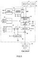
- Fig. 3 shows an internal configuration of the PCM circuit 23.
- the PCM circuit 23 comprises a phase generator 30, an address pointer 31, an interpolation circuit 32, a clip circuit 33, an inverter 34, a low frequency wave generator for amplitude modulation (ALFO) 35, an envelope generator 36, a multiplying circuit 37 and an adder 38.
- the process in the PCM circuit is carried out by the time-shared way of the thirty two channels.
- FNS data, frequency specifying data in an octave, which is corresponding to a tone pitch name and octave data OCT are supplied from the SCPU 12, and the data is set into the phrase generator 30.
- the phrase generator 30 generates phrase data based on the FNS and the OCT for each specified sampling cycle.
- the phrase data is inputted into the address pointer 31.
- the start address data SA, the loop start address data LSA and the loop end address data LEA, which specify a set of PCM wave data, are inputted into the address pointer 31 from the SCPU 12.
- the address pointer 31 decides an incremental amount of an address number according to the phrase data inputted from the phrase generator 30, and outputs the address data including a decimal fraction.
- the decimal fraction data FRA is outputted to the interpolation circuit 32, and two integer addresses MEA between which the FRA is sandwiched are outputted to the DRAM 13 through the memory controller 21.
- the first PCM wave data and the second PCM wave data which is next to the first PCM wave data are read from the DRAM 13 according to the two inputted integer addresses MEA.
- the PCM wave data read from the DRAM 13 is inputted into the interpolation circuit 32 through the memory controller 21.
- the interpolation circuit 32 interpolates the two inputted PCM wave data according to the FRA inputted from the address pointer 31, and generates the digital low frequency signal data.
- the interpolation circuit 32 outputs thus obtained data to the clip circuit 33.
- the clip circuit 33 is a selector which change the output between the digital low frequency signal data inputted from the interpolation circuit 32 and all "0" data, selecting either for the output according to select signal data SSCTL inputted from the SCPU 12.
- the SSCTL is "0"
- the digital low frequency signal data inputted from the interpolation circuit 32 is outputted as it is to the inverter 34. If the SSCTL is "1", the all "0" data is outputted to the inverter 34 in place of the digital low frequency signal data. Because the read data from the DRAM 13 to which the address pointer 31 accesses becomes invalid at all when the SSCTTL is "1”, the SSCTL is supplied to the memory controller as an inhibit data to work. As a result, when the SSCTL is "1" at a channel, there is no access at the channel to the DRAM 13 to thereby make an allowance of a memory cycle.
- the inverter 34 inverts each bit of the digital low frequency signal data which consists of a plurality bits (for example, sixteen bits) according to the SPCTL.
- the SPCTL consists of two bits data inputted from the SCPU.
- the digital low frequency signal data and the SPCTL are inputted into two input terminals of the XOR circuit.
- a higher bit of the SPCTL is inputted into the XOR for a sign bit (the maximum bit) of the digital low frequency signal data, while, a lower bit of the SPCTL is inputted into the XORs for numeral bits (amplitude bits).
- the inputted digital low frequency signal data is outputted as it is, otherwise, if the SPCTL is "1" and "0", the sign bit of the inputted digital low frequency signal data is only inverted to output. Still more, if the SPCTL is "0" and “1”, the numeral bits of the digital low frequency signal data are inverted to output, and if the SPCTL is "1" and "1", all the bits are inverted to output.
- the digital low frequency signal data (including direct current signal data) outputted from the inverter 34 is inputted into a multiplying circuit 39.
- the ALFO 35 and the EG 36 are connected through an adder 38 to the multiplying circuit 39. That is, low frequency signal data generated by the ALFO 35 is inputted into the adder 38, and envelope data generated by the EG 36 is multiplied by total level data TL to output it to the adder 38.
- the added data at the adder 38 is inputted into the multiplying circuit 39 and a comparator 60. If a normal musical tone signal data is inputted as the digital low frequency signal data, the multiplying circuit 39 processes the signal by the amplitude modulation and the envelope imparting.
- the digital low frequency signal data or the envelope data is used as the modulation data at the DSP 24
- the digital low frequency signal data is fixed at a specified value and the output data from the adder 38 is inputted into the multiplying circuit 39.
- the modulation data for imparting the sound effects is inputted as the digital low frequency signal data, the ALFO 35 and the EG 36 are substantially turned off to output the modulation data as it is.
- the clip circuit 33 and the inverter 34 are mainly arranged for the purpose.
- the SSCTL is set to "1" and the SPCTL is set to "0" and "1", for example.
- the output of the clip circuit 33 is fixed to "0, 0.....0”
- the output of the inverter 34 is fixed to the maximum value data "0,1......1”.
- This fixed data is multiplied by the output data of the ALFO 35 or the output data of the EG 36, and therefore the output data of the ALFO 35 or the EG 36 is directly outputted from the multiplying circuit 37.
- the musical tone signal data is inputted into the multiplying circuit 39 as the digital low frequency signal data, and the low frequency wave signal data is inputted from the ALFO 35 into the circuit 39, the inputted musical tone signal data is modulated by the low frequency wave signal data.
- the musical tone signal data is inputted into the multiplying circuit 39 as the digital low frequency signal data, and the envelope wave data is inputted from the EG 36 into the circuit 39, the inputted musical tone signal data is multiplied by the envelope wave data to provide the changing of the tone volume according to the envelope wave data.
- the digital low frequency signal data is fixed (changed) to a specified value at the clip circuit 33, and the low frequency signal data or the envelope wave data is outputted directly from the multiplying circuit 39.
- the ALFO 35 and the EG 36 are substantially set to "OFF" to output the modulation data directly from the multiplying circuit 39.
- the ALFO 35 and the EG 36 are arranged by a well known circuit.
- the ALFO 35 generates the sin curve wave data or the low frequency wave data as shown in Figs. 7A to 7C, for example, according to frequency data LFOS, wave specifying data LFOWS, and influence data (amplitude data) LFOA supplied by the SCPU 12.
- the EG 36 generates the envelope wave data as shown in Fig. 8, according to attack rate data AR, first decay rate data D1R, second decay rate data D2R, and release rate data RR supplied by the SCPU 12.
- the PCM wave data may include the wave data in which an envelope wave is provided to only an attack part, a part from the start address SA to the loop start address LSA. If such PCM wave data is read, the maximum value data is outputted from the EG 36 during the attack part reading (refer to the broken line in Fig. 8).
- the input data from the adder 38 is compared with threshold data TH. If the input data from the adder 38 is smaller than the TH in a processed channel, the INH is outputted to the memory controller 21 since the digital low frequency signal data in the processed channel is not necessary in generating, thereby a memory access of the processed channel being inhibited to free the memory cycle.
- the value of the TH is set, for example, to the minimum decay value of the envelope data.
- Fig. 4 is a block diagram of the DSP 24 which is built into the tone signal generator LSI 11.
- the digital low frequency signal data for the 16 channels inputted from the PCM circuit 23 can be handled at the same time, and also the digital low frequency signal data for the 2 channels inputted from outside can be handled at the same time.
- the DSP 24 processes the inputted data by delaying or filtering if the data is the tone signal data, and outputs thus processed data to the output mixing circuit 25.
- the DSP 24 can process the digital low frequency signal data as the modulation data, i. e., the coefficient data for providing the sound effects, to any tone signal data.
- the PCM circuit 23 has 32 channels while the DSP 24 has 16 channels. This difference in the number of channels may be cancelled by that a part of the output of the DSP 24 is directly outputted to the output mixing circuit 25.
- the DSP24 has a MIXS register 41 of 16 words as a register for storing the inputted digital low frequency signal data from the PCM circuit 23.
- the DSP 24 has also an EXTS register 42 of 2 words as a register for storing the inputted digital low frequency signal data from an external tone generator 18.
- the DSP 24 has still more a MEMS register 43 of 32 words as a register for temporarily storing the data which is read from a ring buffer of the DRAM 13, to process it again by the DSP 24.
- These registers MIXS 41, EXTS 42, and MEMS 43 are connected to both of a register 45 and a selector 48.
- the register 45 is a circuit for temporarily storing the coefficient data (modulation data) to input it to a multiplying circuit 49 in synchronization with the timing of the tone signal data to be modulated.
- the selector 48 is a circuit for selecting the tone signal data to be inputted to the multiplying circuit 49. The combination of the input data to the register 45 and the selector 48 allows the process of the DSP 24 to provide the tone signal data with various sound effects.
- the DSP 24 processes repeatedly the 256 steps of the program stored in a micro program memory 40.
- the program specifies any desired register, from among the registers, MEMS 43, EXTS 42 and MIXS 41, which outputs the data to the register 45 or the selector 48.
- a DRAM address generator 44 generates address data to access the ring buffer in the DRAM 13, and outputs it to the memory controller 21.
- the memory controller 21 access the DRAM 13 by this address data to write/read data to be delayed in the ring buffer.
- the multiplying circuit 49 multiplies the tone signal data by the coefficient data to impart various sound effects to the tone signal data.
- the tone signal data to be modulated is chosen from among the data of the registers, MIXS 41, EXTS 42, MEMS 43 and a TEMP-RAM 53.
- the TEMP-RAM 53 is a temporary RAM register to temporarily store the data once processed by this DSP 24, resulting in short delay.
- the temporarily stored data is inputted for re-processing into the selector 48 or another selector 54 by a feedback circuit.
- the control of the selectors and any other registers is performed by the program.
- the coefficient data to be inputted into the multiplying circuit 49 is chosen by a selector 47.
- the register 45 and a coefficient register 46 in which some fixed coefficient data is stored are connected to the selector 47, and the fixed data "000....1" (i.e., "1" of decimal numeral) is inputted into the selector 47.
- the selector 47 chooses onedata from among these data as the coefficient data to be used, and outputs it to the multiplying circuit 49. If the register 45 is chosen, the digital low frequency signal data inputted from the PCM circuit 23 may be imparted, as the modulation data for the sound effects, to the tone signal data inputted from the selector 48.
- the modulation to the tone signal data is carried out by the fixed coefficient data stored in the coefficient register 46. If the fixed data, "000....1", is chosen in place of these registers, the inputted tone signal data is outputted to the next circuit (an adder 50) as it is.
- the tone signal data outputted from the multiplying circuit 49 is inputted into the adder 50.
- the adder 50 adds the specified coefficient data for adding to the tone signal data, the added data being outputted from this DSP 24 through a 1 clock delay circuit 51 and a shift circuit 52.
- the specified coefficient data for adding is chosen by the selector 54 from among the output of the 1 clock delay circuit 51, the output of the TEMP-RAM 53, and the fixed all "0" data.
- the 1 clock delay circuit 51 is a circuit for delaying the added data for one sampling clock
- the shift circuit 52 is for shifting thus delayed data by a number of specified figures which is set externally.
- the TEMP-RAM 53 delays for a moment the output data of the shift circuit 52 by temporarily storing the data.
- the ring buffer's one from 10 ms to 1s) in the DRAM 13 is longer than the TEMP-RAM's one.
- various sound effects can be imparted to the tone signal data by the delay of the ring buffer, the 1 bit delay circuit 51, and the TEMP-RAM 53, by the multiplying of the multiplying circuit 49, and by the adding of the adder 50. Furthermore, it is optional to select the input data to the multiplying circuit 49, as the tone signal data, from among the digital low frequency signal data, the digital signal data from the external tone signal generator 18, and the delayed digital signal data outputted from the ring buffer in the DRAM 13. Also, it is arbitrary to select the coefficient data for multiplying from among the digital low frequency signal data, the digital signal data from the external tone signal generator 18, the delayed digital signal data outputted from the ring buffer in the DRAM 13, and the fixed coefficient data from the coefficient register 46. This configuration of the DSP 24 allows the sound effects to be much wider, deeper, and more optional.
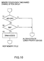
- Fig. 10 is a flow chart showing an access control process of the memory controller. This process belongs to the first priority order of the table shown in Fig. 9.
- the tone generation channel to be accessed is in key-off. If it is in key-off, the lower items in the table become possible to access to any memory.
- the DRAM can be accessed to read the PCM wave data in only case the channel is not in key-off and no INH is inputted (n3).
- the PCM circuit 23 outputs the INH, when the level of the envelope data or the low frequency signal data, for modulation to be multiplied by the digital low frequency signal data, becomes smaller than the specified threshold data TH, and when the SSCTL becomes "1" to thereby fix the digital low frequency signal data, the PCM circuit 23 outputs the memory access inhibit data INH, and therefore, the memory controller 21 inhibits the access to the DRAM 13 in the tone generation channel in response to the INH to free the memory cycle in which any other lower priority items, for example the SCPU 12 or the MCPU 10, can access.
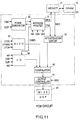
- Fig. 11 shows an internal structure of another type of the PCM circuit 23.
- the PCM circuit 23 comprises the phrase generator 30, the address pointer 31, the interpolation circuit 32, the low frequency wave generator for amplitude modulation (ALFO) 35, the envelope generator (EG) 36, the multiplying circuit 60 and the output controller 61.
- the process in the PCM circuit 23 is carried out by the time-shared way of the thirty two channels.
- FNS data, frequency specifying data in an octave, which is corresponding to a tone pitch name and octave data OCT are supplied from the SCPU 12, and the data is set into the phrase generator 30.
- the phrase generator 30 generates phrase data based on the FNS and the OCT for each specified sampling cycle.
- the phrase data is inputted into the address pointer 31.
- the start address data SA, the loop start address data LSA and the loop end address data LEA, which specify a set of PCM wave data, are inputted into the address pointer 31 from the SCPU 12.
- the address pointer 31 decides an incremental amount of an address number according to the phrase data inputted from the phrase generator 30, and outputs the address data including a decimal fraction.
- the decimal fraction data FRA is outputted to the interpolation circuit 32, and two integer addresses MEA between which the FRA is sandwiched are outputted to the DRAM 13 through the memory controller 21.
- the first PCM wave data and the second PCM wave data which is next to the first PCM wave data are read from the DRAM 13 according to the two inputted integer addresses MEA.
- the PCM wave data read from the DRAM 13 is inputted into the interpolation circuit 32 through the memory controller 21.
- the interpolation circuit 32 interpolates the two inputted PCM wave data according to the FRA inputted from the address pointer 31, and generates the digital low frequency signal data.
- the output of the interpolation circuit 32 is inputted into the multiplying circuit 60 to which the low frequency signal data such as rectangle wave data and saw tooth wave data from the ALFO 35 and the EG 36, or the EG data shown in Fig. 8 is supplied.
- the multiplying circuit 60 processes multiplying for each one word which is a process unit in each time slot to output it to the output controller 38.
- the digital low frequency signal data which is the output of the interpolation circuit 32 is controlled in envelope by the output data of the ALFO 35 and the EG 36, therefore being outputted to the DSP 24 through the output controller 38.
- the DSP 24 operates thus controlled data by filtering, outputting it to the D/A converter 16 for outputting musical tone signals.
- the PCM circuit 23 is provided with a control line for outputting data CHNG from the address pointer to the EG 36.
- the CHNG is data which is generated when the address pointer 31 detects a read end point of the attack phase in the PCM wave data.
- the EG 36 receives the CHNG to control the EG data so that the EG data is changed from the attack phase to the following phase.
- Fig. 12 is a block diagram of the phase generator 30 and the address pointer 31 arranged in the PCM circuit 23.
- the phase generator 30 is provided with a shift circuit 70 and a accumulator 71.
- the shift circuit 70 generates frequency data by shifting the FNS data enough for the OCT data.
- the frequency data is inputted into the accumulator 71 to generate phase data, i.e., relative address data (as the start address SA is "0") to read the PCM wave data.
- the address pointer 31 is equipped with a subtracter 80 for subtracting the loop end address LEA of the loop data area (refer to Fig. 5) from the relative address data outputted from the accumulator 71, an adder 81 for adding the output data other than the sign bit of the subtracter 80 to the loop start address data LSA, a selector for selecting the added data by the adder 81 or the output of the accumulator 71, an adder 83 for adding the output data of the selector 82 to the start address data SA which is absolute address data, an adder 84 and an selector 85 associated with the interpolation circuit 32 for calculating the decimal fraction data FRA, and a comparator 86 for comparing the relative address data with the LSA.
- the SA is given as the absolute address
- the LSA and the LEA being given as the relative address to the SA.
- the address pointer's process is described referring to the addresses in the voice wave data storage area shown in Fig. 5.
- the subtracter 80 subtracts the LEA from the relative address of the accumulator 71, so that the sign bit of the subtracter 80's output is a minus at the beginning of the PCM wave data reading.
- the selector 82 selects the output of the accumulator 71 to output it to the adder 83, when the subtracter 80's output is a minus. Therefore, at the beginning of the PCM wave data reading, the output of the accumulator 71 is outputted to the adder 83 as it is, and then the output of the accumulator 71 is added to the SA which is the absolute start address to output thus added address as actual address of the DRAM 13.
- the added result by the adder 83 is divided into the integer address data MEA and the decimal fraction address data FRA.
- the MEA is outputted trough the selector 85 at the first cycle in one slot as it is, and is added to "1" by the adder 84 at the latter cycle in the same slot to output thus added data through the selector 85.
- the two sets of the MEA are provided to the memory controller 21 in one slot, so that the memory controller 21 receives the two sets of the MEA in one slot, outputting two sets of data corresponding the MEA to the interpolation circuit 32 for interpolation as to the FRA.
- the plus data switches the selector 82, and the accumulator 71 loads the output of the adder 81 because a sign terminal of the subtracter 80 is connected to a load terminal of the accumulator 71.
- the output data other than the sign bit is nearly equal to "0", so that LSA' data which is slightly larger than the LSA is loaded into the accumulator 71.
- the selector 82 selects the output of the accumulator 71 again.
- the selector 82 selects the output of the adder 81 to then output the LSA', and immediately after that, selects again the output of the accumulator 71, thereby an increment amount from the LSA' being outputted to the adder 83.
- repeatedly reading as shown by an arrow in Fig. 5, is performed.
- the relative address data outputted from the accumulator 71 is compared with the LSA by the comparator 86, and when both of the address data coincide, the CHNG is outputted to the EG 36.
- the CHNG output timing is a timing that the output of the accumulator 71 reaches the LSA from the SA.
- the relative address data, the output of the accumulator 71 becomes the LSA' which advances slightly larger than the LSA, then no CHNG being generated at the reach timing.
- the EG data phase is changed from the attack phase to the following phase when the CHNG is generated.
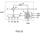
- Fig. 13 is a detail block diagram of the EG 36.
- a selector 90 selects rate data from among “0”, “D1R”, “D2R”, and “RR” and outputs it to a subtracter 92 according to an output of a phase change control circuit 91.
- Each rate data represents a rate change width for each clock.
- the rate data selected by the selector 90 is used first as subtracting data from "0" at the subtracter 92, and then is used as subtracting data from a one clock delay circuit 93 from the next clock cycle.
- the output of the subtracter 92 is equal to the output of the EG, being supplied to the phase change control circuit 91 in order to monitor whether the EG data reaches a decay level DL or not.
- the EG data is also supplied to the delay circuit 93.
- the output of the subtracter 92 i.e., output of the EG 36, decays gradually on the basis of the rate data selected by the selector 90 except the rate being "0". While, the output level of the phase change control circuit 91 is compared with the decay level DL at the timing when the first decay phase changes to the second decay phase in the control circuit 91 to monitor whether both levels coincide or not. If they coincide, the selector 90 is instructed so that the rate data D2R is selected.
- the decay level DL is set beforehand, not key-on data KON or the like generated by events. The key-on data KON, the key-off data KOFF, and the CHNG from the address pointer 31 are inputted into the phase change control circuit 91.
- the phase change control circuit 91 instructs the selector 90 so that "0" is selected when it receives the key-on data KON, then so that D1R being selected when it receives the CHNG from the address pointer 31. Furthermore, the circuit 91 instructs the selector 90 so that RR is selected when it receives the key-off data KOFF.
- the above mentioned control process allows the attack phase of the EG data to be outputted when the KON is inputted first, then the first decay phase D1 to be outputted when the CHNG is inputted from the address pointer 31, further the second decay phase to be outputted when the EG data level reaches the DL, still more the release phase R to be outputted when the KOFF is inputted.
- the timing when the CHNG is outputted from the address pointer 31 is when the comparator 86 detects the coincidence of the relative address data from the accumulator 71 and the LSA. Therefore, because the CHNG is generated when the read address of the PCM wave data reaches the LSA, the EG data generating phase is moved to the first decay phase D1 from the attack phase A in the EG 36, so that the PCM wave data reading and the attack phase generating of the EG data are interlocked. That is, the attack phase length L in Fig. 14 interlocks with the attack phase length of the PCM wave data to thereby allow the attack phase length L to be precisely expanded and contracted according to the musical tone pitch to be generated.
- the reading end address of the attack phase in the musical tone signal data (the PCM wave data) is detected at the address pointer 31, the CHNG is outputted to the EG 36, and the EG data phase is changed from the attack phase to the following phase in response to the CHNG at the EG 36.
- the EG data is precisely interlocked with the musical tone signal data in the attack part to generate the musical tone properly in any pitch changing.
Abstract
Description
- The present invention relates to a tone signal generator which can generate tone signals to which various specialized sound effects such as modulation and pitch change are provided, along with musical tones and normal sound effects, and particularly to improvement in access efficiency to a memory in which the tone signals are stored.
- TV game and electronic musical instruments for entertainment in practical use have tone signal generators. In this instrument, data of tone signals stored in a game cartridge provided by a ROM or a CD - ROM is supplied into an internal RAM of the game instrument, and the data is read according to progress of a game program carried out for generating, musical tones with the normal sound effects and the musical tones as background music.
- There is filter data for imparting various sound effects to tone signal data to be generated in the RAM, along with the above described data, and a buffer area for imparting the sound effects and other areas for storing process data are also assigned in the RAM. Generally, a CPU and other devices in the TV game or musical instrument frequently access the RAM.
- However, the RAM is accessed continuously till a keyoff signal (i.e., a note off signal) is inputted, even though the tone signal in generating becomes the lowest level that no sound is to be substantially heard. The access is apparently unnecessary, thereby causing useless power consumption.
- In order to solve the problem, programmers have made a program so that the key-off signal is generated during the tone signal generation. However, such program has increased loads of programming by the programmer. There are plural ways to deal with the release of unnecessary occupied RAM space.
- US 4,357,849 discloses a key switch information assignor. When a key is depressed or released a keyboard circuit produces respective key information. A data processor then determines whether a these information correspond to either a depression or release of a key and generates a key code combining all key information. This key code is then sent to an assignment memory. An envelope generator determines the end of note sounding, releases the corresponding key code from the assignment memory at the same time, and sends this information back to the data processor. In case all channels of the assignment memory are in use the CPU generates a demand signal interrupting the processing under execution allowing the channels of the assignment memory to be quickly released.
- In US 5,123,323 a method for determining an extreme value channel of an electronic musical instrument is disclosed. In a memory of some musical instruments there are provided several groups of channels storing musical tone information with all of the groups serving different purposes and are therefore assigned independently from each other. The method is capable of detecting the channels of each group containing the musical tone having the highest or lowest level of its envelope signal by using several detector units.
- From US 5,159,144 an electronic musical instrument is known that calculates a in integrated residual envelope volume of musical tones to be allotted to tone generating channels. Whenever all tone generating channels are in use the channel holding the musical tone having the minimum integrated residual volume is then replaced by a musical tone corresponding to a newly depressed key of a keyboard.
- In
EP 0 204 122 an electronic musical instrument is disclosed comprising a keyboard. A CPU assigns key codes to selected tone generating channels of a RAM. Thereby a tone is generated according to the assigned key code. Whenever a new key is pressed down on the keyboard each of the key codes stored in the RAM is fed to an envelope generator to generate data representing the amplitude of the envelopes of the corresponding tone. The CPU modifies these data by using weighting data corresponding to the respective key codes supplied by a ROM. Based on these weighting data the CPU selects the "least important" one replacing it by the data corresponding to the newly depressed key of the keyboard. - Still, all of these prior art devices have to continuously access the channels of the RAM memory in order to determine, erase or release the channel containing the tone signal having the lowest envelope level.
- While, the tone signal generator usually is provided with a generator for generating envelope wave data which is imparted to the tone signal data read from the RAM. Fig. 15 shows an example of the tone signal data, for example, musical tone signal data, and the envelope wave data (EG data). The tone signal data includes attack data arranged in an attack part of the tone signal data, and loop data arranged in the following part. The EG data is divided, as shown in Fig. 15, into four phases, A- attack phase, D- decay phase, S-. sustain phase (or D2. second decay phase), and, R- release phase. when the tone signal data is read, the EG data is supplied to the tone signal data. In Fig. 15, the loop data is arranged between a loop start address LSA and a loop end address LEA, and when the read address reaches the LEA, the read address returns to the LSA, thereby the read address being looped between the LSA and the LEA.
- In the above mentioned tone signal generator, if a pitch is changed, a read address changing width of the tone signal data is changed. That is, if the pitch is changed high, the read address changing width is changed large, and if the pitch is changed low, the read address changing width is changed small.
- However, since a generation speed of the EG data is constant, if the read address changing width is changed according to the pitch changing, the phase change timing from the attack phase to the decay phase in the EG data is mismatched with the phase timing from the attack data to the loop data in the tone signal data. Therefore, a proper tone signal can't be generated.
- In order to solve the problem, a prior tone signal generator is provided with a key scaling way in which a gradient of the attack phase is changed in response to the pitch changing. However, in the key scaling way, it is difficult to keep severe phrase matching between the attack phase in the EG data and the attack data in the tone signal data, and to simplify a structure for changing a shape of the EG data.
- It is therefore an object of the present invention to provide a tone signal generator in which power consumption is minimized.
- It is another object of the present invention to provide a tone signal generator in which memory access is more efficient.
- It is further object of the present invention to provide a tone signal generator which is capable of severely matching the phase timing of the EG data and the tone signal data.
- In accordance with the present invention, an embodiment of it comprises a memory for storing tone signal data, the tone signal data including attack data for an attack phase of the tone signal data and following data for a following phase of the tone signal data; a read controller for reading the tone signal data from the memory; an envelope data generator for generating envelope data corresponding to the attack phase and the following phase of the tone single data; and an envelope imparting circuit for modifying the tone signal data read by the read controller based on the envelope data generated by the envelope data generator, wherein when the read controller ends reading of the attack phase of the tone signal data, a phase of the envelope data generated by the envelope data generator is changed from the attack phase to the following phase in order to match a phase timing of the envelope data and the tone signal data.
- According to a further embodiment of the present invention the read controller generates a control signal when it ends reading of the attack phase of the tone signal data, and a phase change controller changes the phase of the envelope data generated by the envelope data generator from the attack phase to the following phase when the control signal is generated by the read controller.
- In another embodimet of the present invention the tone signal generator may be set up such that the envelope data generator selects a data change rate, before the control signal is generated by the read controller, the envelope data generator selects a first data change rate, and when the control signal is generated by the read controller, the phase change controller changes the phase of the envelope data from the attack phase to the following phase by causing the envelope data generator to select a second data change rate, which is different from the first data change rate.
- This configuration of a tone signal generator allows the phase timing of the envelope data and the tone signal data to be severely matched.
-
- Fig. 1 is a block diagram of a TV game instrument, to which a tone signal generator LSI is applied, embodying the present invention.
- Fig. 2 is a block diagram of the Cone signal generator LSI.
- Fig. 3 is a block diagram of a PCM circuit in the tone signal generator LSI.
- Fig. 4 is a block diagram of a DSP in the tone signal generator LSI.
- Fig. 5 illustrates an internal structure of a DRAM which is connected to the tone signal generator LSI.
- Fig. 6 illustrates a structure of an inverter in the PCM circuit.
- Fig. 7 shows an example of a wave for modulation, which is stored in the DRAM.
- Fig. 8 shows an example of an envelope which is generated by the PCM circuit.
- Fig. 9 shows a priority order table of access to the DRAM.
- Fig. 10 is a flow chart showing a process of a memory controller.
-
- Fig. 1 is a block diagram of a TV game instrument, to which a tone signal generator LSI is applied, embodying the present invention.
- A display 4 and a speaker 5 are connected to a
game instrument 1. The display 4 and the speaker 5 can be used as ones installed into a normal TV receiver. To thegame instrument 1, agame cartridge 3 having aROM 19 in which a game program is stored and acontroller 2 for a player to play a game are also connected. Thecontroller 2 is connected to thegame instrument 1 through a cable or the like, and thegame cartridge 3 is set into a slot mounted in thegame instrument 1. - The
game instrument 1 is equipped with a main CPU (MCPU) 10 which controls a whole program of the game progress. To theMCPU 10, thecontroller 2, theROM 19 mounted into thegame cartridge 3, adisplay controller 14 for controlling the display 4 and a tonesignal generator LSI 11, for generating tone signals, such as musical tone signals, with sound effects and musical tones as a back ground music, are connected. A sound CPU (SCPU) 12, aDRAM 13 in which a program for theSCPU 12 and PCM wave data are stored, and a D/A converter 16, for converting generated musical tone data into analogue musical tone signals, are connected to the tonesignal generator LSI 11. The speaker 5 is connected to the D/A converter 16. The tonesignal generator LSI 11 is provided with an external input terminal into which digital tone data can be inputted from an externaltone signal generator 18. AVRAM 15 in which screen display data is stored and the display 4 are connected to thedisplay controller 14. - When the power turns on after the
game cartridge 3 is set into the game instrument, theMCPU 10 reads specified screen data and sends it to thedisplay controller 14. Then, theMCPU 10 writes programs and the PCM wave data in theDRAM 13, for generating the tone signal data with the sound effects and the BGM (Back Ground Music) tone signal data. After that, the game program is started by operation of thecontroller 2, and the re-writing of the screen data and the generating of the tone signal data with the sound effects and the BGM tone signal data are performed. The progress control of the game program, i.e., re-writing of the screen data, is carried out directly by theMCPU 10. TheMCPU 10 gives instructions to theSCPU 12 for generating the tone signal data with the sound effects and the BGM tone signal data, and the synthesizing of the real tone signal is carried out by theSCPU 12 on the basis of the program and the PCM wave data written into theDRAM 13. - Fig. 2 is an internal block diagram of the tone
signal generator LSI 11. In the tonesignal generator LSI 11, aPCM circuit 23 generates digital low frequency signal data, such as the tone signal data and modulation signal data, when it reads the PCM wave data stored in the DRAM 13 (refer to Fig. 1). As described above, when thegame cartridge 3 is set into the slot and the power is turned on, data is streamed from theROM 19 to theDRAM 13. Therefore, the tone signal data with the sound effects and the BGM tone signal data can be individually different in each game program. To theDRAM 13, theMCPU 10 and theSCPU 12 are connected through amemory controller 21 and aCPU interface 20, and thePCM circuit 23 and a DSP (digital signal processor) 24 mounted into the tonesignal generator LSI 11 are connected through thememory controller 21. TheMCPU 10, theSCPU 12, thePCM circuit 23 and theDSP 24 are individually accessible to theDRAM 13 by sharing time. Aninternal register 22 is connected to theCPU interface 20. Data set into thePCM circuit 23 and theDSP 24, and data for specifying data to set into them by theMCPU 10 and theSCPU 11 are temporarily stored into theinternal register 22. - Fig. 5 shows an internal configuration of the
DRAM 13. - In the
DRAM 13, a SCPU program area for theSCPU 12, a PCM wave data area and a DSP ring buffer are assigned. The PCM wave data includes voice wave data to generate musical tone signals with the sound effects and the BGM tones, and the modulation wave data used as parameters for the sound effects such as the modulation. The plural kinds of voice wave data and the modulation wave data exist and are stored for each data in theDRAM 13. The DSP ring buffer area is used to delay the tone signal data to thereby effect the filtering and the modulating or the like in theDSP 24's process. - As the voice wave data, sampled data of the tone signals with the sound effects or of natural instrument's tone signals is used generally. Such tone signals keep generating tones in long time, so that the voice wave data comprises start address data SA, and the loop start address data LSA and the loop end address data LEA to read repeatedly. First, the SA is read, and then LSA, LEA are read successively and repeatedly. As a result, the repeated reading between the LSA and the LEA allows generating tone signals to be long time. The modulation wave data is generally simple data, such as sin curve wave data or wave data shown in Fig. 7 (Figs. 7A, 7B, 7C), because it is for modulating musical tone signals or the like.
- The SCPU program, the voice wave data and the modulation data are written by the
MCPU 10 when thegame cartridge 3 is set into the slot. TheSCPU 12 processes the SCPU program based on theMCPU 10's instructions. ThePCM circuit 23 reads the PCM wave data based on theSCPU 12's instructions, and generates the digital low frequency signal data. The digital low frequency signal data is used as the tone signal data or the sound effect data. ThePCM circuit 23 has thirty two time sharing channels in which thirty two kinds of the digital low frequency signal data can be generated individually. - Fig. 9 shows a priority order table of access to the
DRAM 13 set in thememory controller 21. The process of the tonesignal generator LSI 11 is time-shared by thirty two time slots in one sampling clock of the PCM wave data. Thememory controller 21 is processed by a memory cycle which is generated by division of the sampling clock into one hundred eight. Therefore, four memory cycles are corresponding to one slot in the tone signal generator. As shown in Fig. 9, four priority orders are set as to the memory access right. In the first priority order, the memory access rights of theDSP 23 and thePCM 24 are assigned alternately, in the second, third and forth priority orders, the memory access rights of a refresh cycle of the DRAM, theMCPU 10, and theSCPU 12 are assigned. Because theDSP 23 and thePCM 24 are required real time processes for the digital low frequency signal data, the highest priority order for them is assigned in the table. - The
PCM circuit 23 generates the digital low frequency signal data by reading the PCM wave data according to instructions of theSCPU 12. The digital low frequency signal data is used as the musical tone signal data such as the BGM data or the modulation data. ThePCM circuit 23 has thirty two time-shared channels, thereby being capable of generating thirty two kinds of the digital low frequency signal data independently. ThePCM circuit 23 independently monitors a level of the digital low frequency signal data every channel, outputting access inhibit signal data INH to thememory controller 21 by judging that no generation of the digital low frequency signal data is necessary any more, when the level becomes less than a specified value. When the INH is received at a channel, thememory controller 21 stops the access to theDRAM 13 as to the channel, and when any memory access is requested from other device or circuit, thememory controller 21 accesses theDRAM 13 in response to the request, thereby, lower items in the memory access priority table being capable of having a chance to access to theDRAM 13. - The tone signal data in the digital low frequency signal data that the
PCM circuit 23 generates is inputted into theDSP 24 or inputted directly into an outmixing circuit OMIX 25. The modulation signal data is inputted into theDSP 24 for coefficients of the sound effects. Usually, the reading data of the voice wave data area is used as the tone signal data, and the reading data of the modulation wave data area is used as the modulation signal data. However, how to use the signal data is free to thereby generate any desired sound effects. For example, it is possible to use the reading data of the voice wave data area as the modulation signal data. Furthermore, theDSP 24 has an outer external terminal into which other tone signal data or other modulation signal data can be inputted. - The
DSP 24 is a circuit for supplying various sound effects, such as modulating, filtering and pitch-changing, to the inputted tone signal data and outputting thus obtained data to the outputmixing circuit OMIX 25. In order to supply the sound effects to the tone signal data, the modulation signal data which is one of the digital low frequency signal data is inputted into theDSP 24, and theDSP 24 uses the modulation signal data as the coefficients for supplying the sound effects. The tone signal data to which the sound effects is supplied by theDSP 24 is inputted into the outputmixing circuit OMIX 25. TheOMIX circuit 25 changes each tone signal data in the thirty two channels to stereo signal data in two channels, and outputs the stereo signal data to the D/A converter circuit 16. - Fig. 3 shows an internal configuration of the
PCM circuit 23. - The
PCM circuit 23 comprises aphase generator 30, anaddress pointer 31, aninterpolation circuit 32, aclip circuit 33, aninverter 34, a low frequency wave generator for amplitude modulation (ALFO) 35, anenvelope generator 36, a multiplyingcircuit 37 and anadder 38. The process in the PCM circuit is carried out by the time-shared way of the thirty two channels. - FNS data, frequency specifying data in an octave, which is corresponding to a tone pitch name and octave data OCT are supplied from the
SCPU 12, and the data is set into thephrase generator 30. Thephrase generator 30 generates phrase data based on the FNS and the OCT for each specified sampling cycle. The phrase data is inputted into theaddress pointer 31. The start address data SA, the loop start address data LSA and the loop end address data LEA, which specify a set of PCM wave data, are inputted into theaddress pointer 31 from theSCPU 12. Theaddress pointer 31 decides an incremental amount of an address number according to the phrase data inputted from thephrase generator 30, and outputs the address data including a decimal fraction. The decimal fraction data FRA is outputted to theinterpolation circuit 32, and two integer addresses MEA between which the FRA is sandwiched are outputted to theDRAM 13 through thememory controller 21. - The first PCM wave data and the second PCM wave data which is next to the first PCM wave data are read from the
DRAM 13 according to the two inputted integer addresses MEA. The PCM wave data read from theDRAM 13 is inputted into theinterpolation circuit 32 through thememory controller 21. Theinterpolation circuit 32 interpolates the two inputted PCM wave data according to the FRA inputted from theaddress pointer 31, and generates the digital low frequency signal data. Theinterpolation circuit 32 outputs thus obtained data to theclip circuit 33. Theclip circuit 33 is a selector which change the output between the digital low frequency signal data inputted from theinterpolation circuit 32 and all "0" data, selecting either for the output according to select signal data SSCTL inputted from theSCPU 12. If the SSCTL is "0", the digital low frequency signal data inputted from theinterpolation circuit 32 is outputted as it is to theinverter 34. If the SSCTL is "1", the all "0" data is outputted to theinverter 34 in place of the digital low frequency signal data. Because the read data from theDRAM 13 to which theaddress pointer 31 accesses becomes invalid at all when the SSCTTL is "1", the SSCTL is supplied to the memory controller as an inhibit data to work. As a result, when the SSCTL is "1" at a channel, there is no access at the channel to theDRAM 13 to thereby make an allowance of a memory cycle. - The
inverter 34, shown in Fig. 6, inverts each bit of the digital low frequency signal data which consists of a plurality bits (for example, sixteen bits) according to the SPCTL. The SPCTL consists of two bits data inputted from the SCPU. The digital low frequency signal data and the SPCTL are inputted into two input terminals of the XOR circuit. A higher bit of the SPCTL is inputted into the XOR for a sign bit (the maximum bit) of the digital low frequency signal data, while, a lower bit of the SPCTL is inputted into the XORs for numeral bits (amplitude bits). If the SPCTL is "0" and "0", the inputted digital low frequency signal data is outputted as it is, otherwise, if the SPCTL is "1" and "0", the sign bit of the inputted digital low frequency signal data is only inverted to output. Still more, if the SPCTL is "0" and "1", the numeral bits of the digital low frequency signal data are inverted to output, and if the SPCTL is "1" and "1", all the bits are inverted to output. - The digital low frequency signal data (including direct current signal data) outputted from the
inverter 34 is inputted into a multiplyingcircuit 39. TheALFO 35 and theEG 36 are connected through anadder 38 to the multiplyingcircuit 39. That is, low frequency signal data generated by theALFO 35 is inputted into theadder 38, and envelope data generated by theEG 36 is multiplied by total level data TL to output it to theadder 38. The added data at theadder 38 is inputted into the multiplyingcircuit 39 and acomparator 60. If a normal musical tone signal data is inputted as the digital low frequency signal data, the multiplyingcircuit 39 processes the signal by the amplitude modulation and the envelope imparting. If the digital low frequency signal data or the envelope data is used as the modulation data at theDSP 24, the digital low frequency signal data is fixed at a specified value and the output data from theadder 38 is inputted into the multiplyingcircuit 39. If the modulation data for imparting the sound effects is inputted as the digital low frequency signal data, theALFO 35 and theEG 36 are substantially turned off to output the modulation data as it is. Theclip circuit 33 and theinverter 34 are mainly arranged for the purpose. - Therefore, if a programmer wants to directly output the wave data of the
ALFO 35 or theEG 36 from the multiplyingcircuit 39, the SSCTL is set to "1" and the SPCTL is set to "0" and "1", for example. This results in that the output of theclip circuit 33 is fixed to "0, 0.....0", and the output of theinverter 34 is fixed to the maximum value data "0,1......1". This fixed data is multiplied by the output data of theALFO 35 or the output data of theEG 36, and therefore the output data of theALFO 35 or theEG 36 is directly outputted from the multiplyingcircuit 37. - At the multiplying
circuit 39, the following process is carried out. - If the musical tone signal data is inputted into the multiplying
circuit 39 as the digital low frequency signal data, and the low frequency wave signal data is inputted from theALFO 35 into thecircuit 39, the inputted musical tone signal data is modulated by the low frequency wave signal data. - If the musical tone signal data is inputted into the multiplying
circuit 39 as the digital low frequency signal data, and the envelope wave data is inputted from theEG 36 into thecircuit 39, the inputted musical tone signal data is multiplied by the envelope wave data to provide the changing of the tone volume according to the envelope wave data. - If the low frequency signal data or the envelope wave data is used directly for the modulation at the
DSP 24, the digital low frequency signal data is fixed (changed) to a specified value at theclip circuit 33, and the low frequency signal data or the envelope wave data is outputted directly from the multiplyingcircuit 39. - If the digital low frequency signal data is used as the modulation data for providing the tone signal data with the sound effects, the
ALFO 35 and theEG 36 are substantially set to "OFF" to output the modulation data directly from the multiplyingcircuit 39. - The
ALFO 35 and theEG 36 are arranged by a well known circuit. TheALFO 35 generates the sin curve wave data or the low frequency wave data as shown in Figs. 7A to 7C, for example, according to frequency data LFOS, wave specifying data LFOWS, and influence data (amplitude data) LFOA supplied by theSCPU 12. TheEG 36 generates the envelope wave data as shown in Fig. 8, according to attack rate data AR, first decay rate data D1R, second decay rate data D2R, and release rate data RR supplied by theSCPU 12. The PCM wave data may include the wave data in which an envelope wave is provided to only an attack part, a part from the start address SA to the loop start address LSA. If such PCM wave data is read, the maximum value data is outputted from theEG 36 during the attack part reading (refer to the broken line in Fig. 8). - At the
comparator 60, the input data from theadder 38 is compared with threshold data TH. If the input data from theadder 38 is smaller than the TH in a processed channel, the INH is outputted to thememory controller 21 since the digital low frequency signal data in the processed channel is not necessary in generating, thereby a memory access of the processed channel being inhibited to free the memory cycle. In this example, the value of the TH is set, for example, to the minimum decay value of the envelope data. - It is possible to use a multiplying circuit in place of the
adder 38. - Fig. 4 is a block diagram of the
DSP 24 which is built into the tonesignal generator LSI 11. - In the
DSP 24, the digital low frequency signal data for the 16 channels inputted from thePCM circuit 23 can be handled at the same time, and also the digital low frequency signal data for the 2 channels inputted from outside can be handled at the same time. TheDSP 24 processes the inputted data by delaying or filtering if the data is the tone signal data, and outputs thus processed data to theoutput mixing circuit 25. Furthermore, theDSP 24 can process the digital low frequency signal data as the modulation data, i. e., the coefficient data for providing the sound effects, to any tone signal data. - In this embodiment, the
PCM circuit 23 has 32 channels while theDSP 24 has 16 channels. This difference in the number of channels may be cancelled by that a part of the output of theDSP 24 is directly outputted to theoutput mixing circuit 25. - The DSP24 has a
MIXS register 41 of 16 words as a register for storing the inputted digital low frequency signal data from thePCM circuit 23. TheDSP 24 has also anEXTS register 42 of 2 words as a register for storing the inputted digital low frequency signal data from anexternal tone generator 18. TheDSP 24 has still more aMEMS register 43 of 32 words as a register for temporarily storing the data which is read from a ring buffer of theDRAM 13, to process it again by theDSP 24. These registers MIXS 41,EXTS 42, andMEMS 43 are connected to both of aregister 45 and aselector 48. Theregister 45 is a circuit for temporarily storing the coefficient data (modulation data) to input it to a multiplyingcircuit 49 in synchronization with the timing of the tone signal data to be modulated. Theselector 48 is a circuit for selecting the tone signal data to be inputted to the multiplyingcircuit 49. The combination of the input data to theregister 45 and theselector 48 allows the process of theDSP 24 to provide the tone signal data with various sound effects. - The
DSP 24 processes repeatedly the 256 steps of the program stored in amicro program memory 40. The program specifies any desired register, from among the registers,MEMS 43,EXTS 42 andMIXS 41, which outputs the data to theregister 45 or theselector 48. - A
DRAM address generator 44 generates address data to access the ring buffer in theDRAM 13, and outputs it to thememory controller 21. Thememory controller 21 access theDRAM 13 by this address data to write/read data to be delayed in the ring buffer. The multiplyingcircuit 49, as described above, multiplies the tone signal data by the coefficient data to impart various sound effects to the tone signal data. The tone signal data to be modulated is chosen from among the data of the registers,MIXS 41,EXTS 42,MEMS 43 and a TEMP-RAM 53. The TEMP-RAM 53 is a temporary RAM register to temporarily store the data once processed by thisDSP 24, resulting in short delay. The temporarily stored data is inputted for re-processing into theselector 48 or anotherselector 54 by a feedback circuit. The control of the selectors and any other registers is performed by the program. The coefficient data to be inputted into the multiplyingcircuit 49 is chosen by a selector 47. Theregister 45 and acoefficient register 46 in which some fixed coefficient data is stored are connected to the selector 47, and the fixed data "000....1" (i.e., "1" of decimal numeral) is inputted into the selector 47. The selector 47 chooses onedata from among these data as the coefficient data to be used, and outputs it to the multiplyingcircuit 49. If theregister 45 is chosen, the digital low frequency signal data inputted from thePCM circuit 23 may be imparted, as the modulation data for the sound effects, to the tone signal data inputted from theselector 48. If thecoefficient register 46 is chosen in place of theregister 45, the modulation to the tone signal data is carried out by the fixed coefficient data stored in thecoefficient register 46. If the fixed data, "000....1", is chosen in place of these registers, the inputted tone signal data is outputted to the next circuit (an adder 50) as it is. - The tone signal data outputted from the multiplying
circuit 49 is inputted into theadder 50. Theadder 50 adds the specified coefficient data for adding to the tone signal data, the added data being outputted from thisDSP 24 through a 1clock delay circuit 51 and ashift circuit 52. The specified coefficient data for adding is chosen by theselector 54 from among the output of the 1clock delay circuit 51, the output of the TEMP-RAM 53, and the fixed all "0" data. The 1clock delay circuit 51 is a circuit for delaying the added data for one sampling clock, and theshift circuit 52 is for shifting thus delayed data by a number of specified figures which is set externally. The TEMP-RAM 53 delays for a moment the output data of theshift circuit 52 by temporarily storing the data. As to the delay of data, the ring buffer's one (from 10 ms to 1s) in theDRAM 13 is longer than the TEMP-RAM's one. - In the
DSP 24, various sound effects can be imparted to the tone signal data by the delay of the ring buffer, the 1bit delay circuit 51, and the TEMP-RAM 53, by the multiplying of the multiplyingcircuit 49, and by the adding of theadder 50. Furthermore, it is optional to select the input data to the multiplyingcircuit 49, as the tone signal data, from among the digital low frequency signal data, the digital signal data from the externaltone signal generator 18, and the delayed digital signal data outputted from the ring buffer in theDRAM 13. Also, it is arbitrary to select the coefficient data for multiplying from among the digital low frequency signal data, the digital signal data from the externaltone signal generator 18, the delayed digital signal data outputted from the ring buffer in theDRAM 13, and the fixed coefficient data from thecoefficient register 46. This configuration of theDSP 24 allows the sound effects to be much wider, deeper, and more optional. - Fig. 10 is a flow chart showing an access control process of the memory controller. This process belongs to the first priority order of the table shown in Fig. 9. At step n1, the tone generation channel to be accessed is in key-off. If it is in key-off, the lower items in the table become possible to access to any memory. At step n2, whether or not the INH has been inputted from the
PCM circuit 23 is judged. With INH = "yes", the lower items in the table become possible to access to any memory, even though the channel is not in key-off. The DRAM can be accessed to read the PCM wave data in only case the channel is not in key-off and no INH is inputted (n3). - As described above, in this embodiment, the
PCM circuit 23 outputs the INH, when the level of the envelope data or the low frequency signal data, for modulation to be multiplied by the digital low frequency signal data, becomes smaller than the specified threshold data TH, and when the SSCTL becomes "1" to thereby fix the digital low frequency signal data, thePCM circuit 23 outputs the memory access inhibit data INH, and therefore, thememory controller 21 inhibits the access to theDRAM 13 in the tone generation channel in response to the INH to free the memory cycle in which any other lower priority items, for example theSCPU 12 or theMCPU 10, can access. - Another embodiment of the present invention is described as follows, referring to Figs. 11 to 14.
- Fig. 11 shows an internal structure of another type of the
PCM circuit 23. - The
PCM circuit 23 comprises thephrase generator 30, theaddress pointer 31, theinterpolation circuit 32, the low frequency wave generator for amplitude modulation (ALFO) 35, the envelope generator (EG) 36, the multiplyingcircuit 60 and theoutput controller 61. The process in thePCM circuit 23 is carried out by the time-shared way of the thirty two channels. - FNS data, frequency specifying data in an octave, which is corresponding to a tone pitch name and octave data OCT are supplied from the
SCPU 12, and the data is set into thephrase generator 30. Thephrase generator 30 generates phrase data based on the FNS and the OCT for each specified sampling cycle. The phrase data is inputted into theaddress pointer 31. The start address data SA, the loop start address data LSA and the loop end address data LEA, which specify a set of PCM wave data, are inputted into theaddress pointer 31 from theSCPU 12. Theaddress pointer 31 decides an incremental amount of an address number according to the phrase data inputted from thephrase generator 30, and outputs the address data including a decimal fraction. The decimal fraction data FRA is outputted to theinterpolation circuit 32, and two integer addresses MEA between which the FRA is sandwiched are outputted to theDRAM 13 through thememory controller 21. - The first PCM wave data and the second PCM wave data which is next to the first PCM wave data are read from the
DRAM 13 according to the two inputted integer addresses MEA. The PCM wave data read from theDRAM 13 is inputted into theinterpolation circuit 32 through thememory controller 21. Theinterpolation circuit 32 interpolates the two inputted PCM wave data according to the FRA inputted from theaddress pointer 31, and generates the digital low frequency signal data. - The output of the
interpolation circuit 32 is inputted into the multiplyingcircuit 60 to which the low frequency signal data such as rectangle wave data and saw tooth wave data from the ALFO 35 and theEG 36, or the EG data shown in Fig. 8 is supplied. The multiplyingcircuit 60 processes multiplying for each one word which is a process unit in each time slot to output it to theoutput controller 38. The digital low frequency signal data which is the output of theinterpolation circuit 32 is controlled in envelope by the output data of theALFO 35 and theEG 36, therefore being outputted to theDSP 24 through theoutput controller 38. - The
DSP 24 operates thus controlled data by filtering, outputting it to the D/A converter 16 for outputting musical tone signals. - The
PCM circuit 23 is provided with a control line for outputting data CHNG from the address pointer to theEG 36. The CHNG is data which is generated when theaddress pointer 31 detects a read end point of the attack phase in the PCM wave data. As described later, theEG 36 receives the CHNG to control the EG data so that the EG data is changed from the attack phase to the following phase. - Fig. 12 is a block diagram of the
phase generator 30 and theaddress pointer 31 arranged in thePCM circuit 23. - The
phase generator 30 is provided with ashift circuit 70 and aaccumulator 71. Theshift circuit 70 generates frequency data by shifting the FNS data enough for the OCT data. The frequency data is inputted into theaccumulator 71 to generate phase data, i.e., relative address data (as the start address SA is "0") to read the PCM wave data. - The
address pointer 31 is equipped with asubtracter 80 for subtracting the loop end address LEA of the loop data area (refer to Fig. 5) from the relative address data outputted from theaccumulator 71, anadder 81 for adding the output data other than the sign bit of thesubtracter 80 to the loop start address data LSA, a selector for selecting the added data by theadder 81 or the output of theaccumulator 71, anadder 83 for adding the output data of theselector 82 to the start address data SA which is absolute address data, anadder 84 and anselector 85 associated with theinterpolation circuit 32 for calculating the decimal fraction data FRA, and acomparator 86 for comparing the relative address data with the LSA. The SA is given as the absolute address, the LSA and the LEA being given as the relative address to the SA. - The address pointer's process is described referring to the addresses in the voice wave data storage area shown in Fig. 5.
- The
subtracter 80 subtracts the LEA from the relative address of theaccumulator 71, so that the sign bit of thesubtracter 80's output is a minus at the beginning of the PCM wave data reading. Theselector 82 selects the output of theaccumulator 71 to output it to theadder 83, when thesubtracter 80's output is a minus. Therefore, at the beginning of the PCM wave data reading, the output of theaccumulator 71 is outputted to theadder 83 as it is, and then the output of theaccumulator 71 is added to the SA which is the absolute start address to output thus added address as actual address of theDRAM 13. The added result by theadder 83 is divided into the integer address data MEA and the decimal fraction address data FRA. The MEA is outputted trough theselector 85 at the first cycle in one slot as it is, and is added to "1" by theadder 84 at the latter cycle in the same slot to output thus added data through theselector 85. The two sets of the MEA are provided to thememory controller 21 in one slot, so that thememory controller 21 receives the two sets of the MEA in one slot, outputting two sets of data corresponding the MEA to theinterpolation circuit 32 for interpolation as to the FRA. - When the sign bit of the output of the
subtracter 80 changes to a plus, the plus data switches theselector 82, and theaccumulator 71 loads the output of theadder 81 because a sign terminal of thesubtracter 80 is connected to a load terminal of theaccumulator 71. At that timing, the output data other than the sign bit is nearly equal to "0", so that LSA' data which is slightly larger than the LSA is loaded into theaccumulator 71. When the LSA' is loaded into theaccumulator 71, the output sign bit of thesubtracter 80 becomes a minus again. Then, theselector 82 selects the output of theaccumulator 71 again. Therefore, when the relative address of the accumulator output exceeds the LEA, theselector 82 selects the output of theadder 81 to then output the LSA', and immediately after that, selects again the output of theaccumulator 71, thereby an increment amount from the LSA' being outputted to theadder 83. As a result, repeatedly reading, as shown by an arrow in Fig. 5, is performed. - The relative address data outputted from the
accumulator 71 is compared with the LSA by thecomparator 86, and when both of the address data coincide, the CHNG is outputted to theEG 36. The CHNG output timing is a timing that the output of theaccumulator 71 reaches the LSA from the SA. In the loop process, when the address returns to the LSA' from the LEA, the relative address data, the output of theaccumulator 71, becomes the LSA' which advances slightly larger than the LSA, then no CHNG being generated at the reach timing. As described later, the EG data phase is changed from the attack phase to the following phase when the CHNG is generated. - Fig. 13 is a detail block diagram of the
EG 36. Aselector 90 selects rate data from among "0", "D1R", "D2R", and "RR" and outputs it to asubtracter 92 according to an output of a phasechange control circuit 91. Each rate data represents a rate change width for each clock. The rate data selected by theselector 90 is used first as subtracting data from "0" at thesubtracter 92, and then is used as subtracting data from a oneclock delay circuit 93 from the next clock cycle. The output of thesubtracter 92 is equal to the output of the EG, being supplied to the phasechange control circuit 91 in order to monitor whether the EG data reaches a decay level DL or not. The EG data is also supplied to thedelay circuit 93. - In the above mentioned structure, the output of the
subtracter 92, i.e., output of theEG 36, decays gradually on the basis of the rate data selected by theselector 90 except the rate being "0". While, the output level of the phasechange control circuit 91 is compared with the decay level DL at the timing when the first decay phase changes to the second decay phase in thecontrol circuit 91 to monitor whether both levels coincide or not. If they coincide, theselector 90 is instructed so that the rate data D2R is selected. The decay level DL is set beforehand, not key-on data KON or the like generated by events. The key-on data KON, the key-off data KOFF, and the CHNG from theaddress pointer 31 are inputted into the phasechange control circuit 91. The phasechange control circuit 91 instructs theselector 90 so that "0" is selected when it receives the key-on data KON, then so that D1R being selected when it receives the CHNG from theaddress pointer 31. Furthermore, thecircuit 91 instructs theselector 90 so that RR is selected when it receives the key-off data KOFF. The above mentioned control process allows the attack phase of the EG data to be outputted when the KON is inputted first, then the first decay phase D1 to be outputted when the CHNG is inputted from theaddress pointer 31, further the second decay phase to be outputted when the EG data level reaches the DL, still more the release phase R to be outputted when the KOFF is inputted. - In the above described control, the timing when the CHNG is outputted from the
address pointer 31 is when thecomparator 86 detects the coincidence of the relative address data from theaccumulator 71 and the LSA. Therefore, because the CHNG is generated when the read address of the PCM wave data reaches the LSA, the EG data generating phase is moved to the first decay phase D1 from the attack phase A in theEG 36, so that the PCM wave data reading and the attack phase generating of the EG data are interlocked. That is, the attack phase length L in Fig. 14 interlocks with the attack phase length of the PCM wave data to thereby allow the attack phase length L to be precisely expanded and contracted according to the musical tone pitch to be generated. - As described above, the reading end address of the attack phase in the musical tone signal data (the PCM wave data) is detected at the
address pointer 31, the CHNG is outputted to theEG 36, and the EG data phase is changed from the attack phase to the following phase in response to the CHNG at theEG 36. As a result, the EG data is precisely interlocked with the musical tone signal data in the attack part to generate the musical tone properly in any pitch changing.
Claims (3)
- A tone signal generator comprising:a memory (13) for storing tone signal data, the tone signal data including attack data for an attack phase of the tone signal data and following data for a following phase of the tone signal data;a read controller (23) for reading the tone signal data from the memory;an envelope data generator (36) for generating envelope data corresponding to the attack phase and the following phase of the tone single data; andan envelope imparting circuit (24) for modifying the tone signal data read by the read controller (23) based on the envelope data generated by the envelope data generator(36),
wherein when the read controller (23) ends reading of the attack phase of the tone signal data, a phase of the envelope data generated by the envelope data generator (36) is changed from the attack phase to the following phase in order to match a phase timing of the envelope data and the tone signal data. - The tone signal generator as defined in claim 1,
wherein the read controller (23) generates a control signal when it ends reading of the attack phase of the tone signal data, anda phase change controller (91) changes the phase of the envelope data generated by the envelope data generator (36) from the attack phase to the following phase when the control signal is generated by the read controller (23). - The tone signal generator as defined in claim 2,
wherein the envelope data generator (36) selects a data change rate,before the control signal is generated by the read controller (23), the envelope data generator (36) selects a first data change rate, andwhen the control signal is generated by the read controller, the phase change controller (91) changes the phase of the envelope data from the attack phase to the following phase by causing the envelope data generator (36) to select a second data change rate, which is different from the first data change rate.
Applications Claiming Priority (5)
| Application Number | Priority Date | Filing Date | Title |
|---|---|---|---|
| JP6256494 | 1994-03-31 | ||
| JP06256494A JP3588815B2 (en) | 1994-03-31 | 1994-03-31 | Sound source device |
| JP06256194A JP3520553B2 (en) | 1994-03-31 | 1994-03-31 | Sound source device |
| JP6256194 | 1994-03-31 | ||
| EP95104329A EP0675482B1 (en) | 1994-03-31 | 1995-03-23 | Tone signal generator having a sound effect function |
Related Parent Applications (1)
| Application Number | Title | Priority Date | Filing Date |
|---|---|---|---|
| EP95104329A Division EP0675482B1 (en) | 1994-03-31 | 1995-03-23 | Tone signal generator having a sound effect function |
Publications (3)
| Publication Number | Publication Date |
|---|---|
| EP0947979A2 true EP0947979A2 (en) | 1999-10-06 |
| EP0947979A3 EP0947979A3 (en) | 1999-10-13 |
| EP0947979B1 EP0947979B1 (en) | 2007-05-02 |
Family
ID=26403605
Family Applications (2)
| Application Number | Title | Priority Date | Filing Date |
|---|---|---|---|
| EP99111094A Expired - Lifetime EP0947979B1 (en) | 1994-03-31 | 1995-03-23 | Tone signal generator having a sound effect function |
| EP95104329A Expired - Lifetime EP0675482B1 (en) | 1994-03-31 | 1995-03-23 | Tone signal generator having a sound effect function |
Family Applications After (1)
| Application Number | Title | Priority Date | Filing Date |
|---|---|---|---|
| EP95104329A Expired - Lifetime EP0675482B1 (en) | 1994-03-31 | 1995-03-23 | Tone signal generator having a sound effect function |
Country Status (8)
| Country | Link |
|---|---|
| US (1) | US5741991A (en) |
| EP (2) | EP0947979B1 (en) |
| KR (1) | KR100236786B1 (en) |
| CN (1) | CN1052090C (en) |
| BR (1) | BR9501409A (en) |
| DE (2) | DE69535489T2 (en) |
| ES (2) | ES2284227T3 (en) |
| TW (1) | TW281747B (en) |
Families Citing this family (3)
| Publication number | Priority date | Publication date | Assignee | Title |
|---|---|---|---|---|
| US8180063B2 (en) * | 2007-03-30 | 2012-05-15 | Audiofile Engineering Llc | Audio signal processing system for live music performance |
| US20150382129A1 (en) * | 2014-06-30 | 2015-12-31 | Microsoft Corporation | Driving parametric speakers as a function of tracked user location |
| IT202000004231A1 (en) * | 2020-02-28 | 2021-08-28 | St Microelectronics Srl | WAVE FORMS GENERATOR |
Citations (1)
| Publication number | Priority date | Publication date | Assignee | Title |
|---|---|---|---|---|
| US4067253A (en) * | 1976-04-02 | 1978-01-10 | The Wurlitzer Company | Electronic tone-generating system |
Family Cites Families (8)
| Publication number | Priority date | Publication date | Assignee | Title |
|---|---|---|---|---|
| JPS5583095A (en) * | 1978-12-18 | 1980-06-23 | Kawai Musical Instr Mfg Co | Allocating device for keyboarddswitch information |
| DE3688716T2 (en) * | 1985-04-24 | 1994-03-10 | Yamaha Corp | Electronic musical instrument. |
| US5292997A (en) * | 1989-08-17 | 1994-03-08 | Yamaha Corporation | Touch responsive envelope shape generation device |
| JPH0833734B2 (en) * | 1989-10-11 | 1996-03-29 | ヤマハ株式会社 | Extreme value channel designation method for electronic musical instruments |
| US5159144A (en) * | 1990-06-29 | 1992-10-27 | Roland Corporation | Electronic musical instrument employing tone generator selection based on integrated residual envelope volume |
| JPH04115295A (en) * | 1990-09-06 | 1992-04-16 | Yamaha Corp | Musical sound controller |
| JPH056179A (en) * | 1991-06-27 | 1993-01-14 | Kawai Musical Instr Mfg Co Ltd | Musical note channel allocating device |
| JP2671747B2 (en) * | 1993-04-27 | 1997-10-29 | ヤマハ株式会社 | Musical tone forming device |
-
1994
- 1994-11-14 TW TW083110503A patent/TW281747B/zh not_active IP Right Cessation
-
1995
- 1995-03-23 EP EP99111094A patent/EP0947979B1/en not_active Expired - Lifetime
- 1995-03-23 EP EP95104329A patent/EP0675482B1/en not_active Expired - Lifetime
- 1995-03-23 DE DE69535489T patent/DE69535489T2/en not_active Expired - Lifetime
- 1995-03-23 DE DE69514562T patent/DE69514562T2/en not_active Expired - Lifetime
- 1995-03-23 ES ES99111094T patent/ES2284227T3/en not_active Expired - Lifetime
- 1995-03-23 ES ES95104329T patent/ES2141270T3/en not_active Expired - Lifetime
- 1995-03-31 US US08/414,929 patent/US5741991A/en not_active Expired - Lifetime
- 1995-03-31 KR KR1019950007686A patent/KR100236786B1/en not_active IP Right Cessation
- 1995-03-31 CN CN95104586A patent/CN1052090C/en not_active Expired - Fee Related
- 1995-03-31 BR BR9501409A patent/BR9501409A/en not_active IP Right Cessation
Patent Citations (1)
| Publication number | Priority date | Publication date | Assignee | Title |
|---|---|---|---|---|
| US4067253A (en) * | 1976-04-02 | 1978-01-10 | The Wurlitzer Company | Electronic tone-generating system |
Also Published As
| Publication number | Publication date |
|---|---|
| EP0947979A3 (en) | 1999-10-13 |
| ES2141270T3 (en) | 2000-03-16 |
| BR9501409A (en) | 1996-04-09 |
| DE69514562T2 (en) | 2000-09-14 |
| CN1117635A (en) | 1996-02-28 |
| DE69514562D1 (en) | 2000-02-24 |
| DE69535489T2 (en) | 2008-01-10 |
| KR100236786B1 (en) | 2000-01-15 |
| EP0675482A1 (en) | 1995-10-04 |
| KR950033760A (en) | 1995-12-26 |
| US5741991A (en) | 1998-04-21 |
| EP0675482B1 (en) | 2000-01-19 |
| EP0947979B1 (en) | 2007-05-02 |
| DE69535489D1 (en) | 2007-06-14 |
| CN1052090C (en) | 2000-05-03 |
| ES2284227T3 (en) | 2007-11-01 |
| TW281747B (en) | 1996-07-21 |
Similar Documents
| Publication | Publication Date | Title |
|---|---|---|
| US4649783A (en) | Wavetable-modification instrument and method for generating musical sound | |
| KR0160493B1 (en) | Digital audio signal generating apparatus | |
| US5432293A (en) | Waveform generation device capable of reading waveform memory in plural modes | |
| US4726276A (en) | Slur effect pitch control in an electronic musical instrument | |
| JPH0772829B2 (en) | Parameter supply device for electronic musical instruments | |
| US5703312A (en) | Electronic musical instrument and signal processor having a tonal effect imparting function | |
| JPH0412476B2 (en) | ||
| US6091012A (en) | Tone effect imparting apparatus | |
| US5869781A (en) | Tone signal generator having a sound effect function | |
| EP0675482B1 (en) | Tone signal generator having a sound effect function | |
| JPH0254559B2 (en) | ||
| EP0124197A2 (en) | Waveform table modification instrument and method for generating musical sound | |
| JPH0213799B2 (en) | ||
| JP2606918B2 (en) | Music information calculation method | |
| US6972362B2 (en) | Method and device for generating electronic sounds and portable apparatus utilizing such device and method | |
| JPH0310959B2 (en) | ||
| JP3588815B2 (en) | Sound source device | |
| JP3552265B2 (en) | Sound source device and audio signal forming method | |
| JP3520553B2 (en) | Sound source device | |
| JPH0125079B2 (en) | ||
| JPH09269779A (en) | Effect adding device | |
| JP3129119B2 (en) | Envelope waveform generator | |
| JPS6352399B2 (en) | ||
| JP2763535B2 (en) | Electronic musical instrument | |
| JPH021314B2 (en) |
Legal Events
| Date | Code | Title | Description |
|---|---|---|---|
| PUAI | Public reference made under article 153(3) epc to a published international application that has entered the european phase |
Free format text: ORIGINAL CODE: 0009012 |
|
| PUAL | Search report despatched |
Free format text: ORIGINAL CODE: 0009013 |
|
| 17P | Request for examination filed |
Effective date: 19990617 |
|
| AC | Divisional application: reference to earlier application |
Ref document number: 675482 Country of ref document: EP |
|
| AK | Designated contracting states |
Kind code of ref document: A2 Designated state(s): DE ES FR GB IT |
|
| AK | Designated contracting states |
Kind code of ref document: A3 Designated state(s): DE ES FR GB IT |
|
| GRAP | Despatch of communication of intention to grant a patent |
Free format text: ORIGINAL CODE: EPIDOSNIGR1 |
|
| GRAS | Grant fee paid |
Free format text: ORIGINAL CODE: EPIDOSNIGR3 |
|
| GRAA | (expected) grant |
Free format text: ORIGINAL CODE: 0009210 |
|
| AC | Divisional application: reference to earlier application |
Ref document number: 0675482 Country of ref document: EP Kind code of ref document: P |
|
| AK | Designated contracting states |
Kind code of ref document: B1 Designated state(s): DE ES FR GB IT |
|
| REG | Reference to a national code |
Ref country code: GB Ref legal event code: FG4D |
|
| REF | Corresponds to: |
Ref document number: 69535489 Country of ref document: DE Date of ref document: 20070614 Kind code of ref document: P |
|
| RAP2 | Party data changed (patent owner data changed or rights of a patent transferred) |
Owner name: YAMAHA CORPORATION |
|
| REG | Reference to a national code |
Ref country code: ES Ref legal event code: FG2A Ref document number: 2284227 Country of ref document: ES Kind code of ref document: T3 |
|
| ET | Fr: translation filed | ||
| PLBE | No opposition filed within time limit |
Free format text: ORIGINAL CODE: 0009261 |
|
| STAA | Information on the status of an ep patent application or granted ep patent |
Free format text: STATUS: NO OPPOSITION FILED WITHIN TIME LIMIT |
|
| 26N | No opposition filed |
Effective date: 20080205 |
|
| PGFP | Annual fee paid to national office [announced via postgrant information from national office to epo] |
Ref country code: ES Payment date: 20100408 Year of fee payment: 16 |
|
| PGFP | Annual fee paid to national office [announced via postgrant information from national office to epo] |
Ref country code: FR Payment date: 20110317 Year of fee payment: 17 |
|
| PGFP | Annual fee paid to national office [announced via postgrant information from national office to epo] |
Ref country code: GB Payment date: 20110323 Year of fee payment: 17 Ref country code: DE Payment date: 20110316 Year of fee payment: 17 |
|
| PGFP | Annual fee paid to national office [announced via postgrant information from national office to epo] |
Ref country code: IT Payment date: 20110325 Year of fee payment: 17 |
|
| REG | Reference to a national code |
Ref country code: ES Ref legal event code: FD2A Effective date: 20120509 |
|
| PG25 | Lapsed in a contracting state [announced via postgrant information from national office to epo] |
Ref country code: ES Free format text: LAPSE BECAUSE OF NON-PAYMENT OF DUE FEES Effective date: 20110324 |
|
| GBPC | Gb: european patent ceased through non-payment of renewal fee |
Effective date: 20120323 |
|
| REG | Reference to a national code |
Ref country code: FR Ref legal event code: ST Effective date: 20121130 |
|
| PG25 | Lapsed in a contracting state [announced via postgrant information from national office to epo] |
Ref country code: GB Free format text: LAPSE BECAUSE OF NON-PAYMENT OF DUE FEES Effective date: 20120323 Ref country code: FR Free format text: LAPSE BECAUSE OF NON-PAYMENT OF DUE FEES Effective date: 20120402 |
|
| REG | Reference to a national code |
Ref country code: DE Ref legal event code: R119 Ref document number: 69535489 Country of ref document: DE Effective date: 20121002 |
|
| PG25 | Lapsed in a contracting state [announced via postgrant information from national office to epo] |
Ref country code: IT Free format text: LAPSE BECAUSE OF NON-PAYMENT OF DUE FEES Effective date: 20120323 |
|
| PG25 | Lapsed in a contracting state [announced via postgrant information from national office to epo] |
Ref country code: DE Free format text: LAPSE BECAUSE OF NON-PAYMENT OF DUE FEES Effective date: 20121002 |