EP0947864B1 - Breitbandiges Gitter mit langer Periode - Google Patents
Breitbandiges Gitter mit langer Periode Download PDFInfo
- Publication number
- EP0947864B1 EP0947864B1 EP99302188A EP99302188A EP0947864B1 EP 0947864 B1 EP0947864 B1 EP 0947864B1 EP 99302188 A EP99302188 A EP 99302188A EP 99302188 A EP99302188 A EP 99302188A EP 0947864 B1 EP0947864 B1 EP 0947864B1
- Authority
- EP
- European Patent Office
- Prior art keywords
- optical
- long
- region
- grating
- wavelength
- Prior art date
- Legal status (The legal status is an assumption and is not a legal conclusion. Google has not performed a legal analysis and makes no representation as to the accuracy of the status listed.)
- Expired - Lifetime
Links
- 230000003287 optical effect Effects 0.000 claims description 26
- 238000010168 coupling process Methods 0.000 claims description 10
- 238000005859 coupling reaction Methods 0.000 claims description 10
- 238000005253 cladding Methods 0.000 claims description 9
- 230000008878 coupling Effects 0.000 claims description 9
- 238000004891 communication Methods 0.000 claims description 8
- 239000013307 optical fiber Substances 0.000 claims description 6
- 230000003595 spectral effect Effects 0.000 claims description 5
- 230000001419 dependent effect Effects 0.000 claims description 4
- 230000005540 biological transmission Effects 0.000 claims description 3
- 239000002131 composite material Substances 0.000 claims description 2
- 239000000835 fiber Substances 0.000 description 33
- 238000013461 design Methods 0.000 description 15
- 239000006185 dispersion Substances 0.000 description 8
- 238000000411 transmission spectrum Methods 0.000 description 7
- 238000000034 method Methods 0.000 description 6
- VYPSYNLAJGMNEJ-UHFFFAOYSA-N Silicium dioxide Chemical compound O=[Si]=O VYPSYNLAJGMNEJ-UHFFFAOYSA-N 0.000 description 4
- 238000006243 chemical reaction Methods 0.000 description 4
- 230000008901 benefit Effects 0.000 description 3
- 230000008859 change Effects 0.000 description 3
- 238000005516 engineering process Methods 0.000 description 3
- 229910052732 germanium Inorganic materials 0.000 description 3
- GNPVGFCGXDBREM-UHFFFAOYSA-N germanium atom Chemical compound [Ge] GNPVGFCGXDBREM-UHFFFAOYSA-N 0.000 description 3
- 230000000737 periodic effect Effects 0.000 description 3
- 229910052761 rare earth metal Inorganic materials 0.000 description 3
- 150000002910 rare earth metals Chemical class 0.000 description 3
- 229910052691 Erbium Inorganic materials 0.000 description 2
- 238000004364 calculation method Methods 0.000 description 2
- UYAHIZSMUZPPFV-UHFFFAOYSA-N erbium Chemical compound [Er] UYAHIZSMUZPPFV-UHFFFAOYSA-N 0.000 description 2
- 230000010287 polarization Effects 0.000 description 2
- 239000000377 silicon dioxide Substances 0.000 description 2
- UFHFLCQGNIYNRP-UHFFFAOYSA-N Hydrogen Chemical compound [H][H] UFHFLCQGNIYNRP-UHFFFAOYSA-N 0.000 description 1
- OAICVXFJPJFONN-UHFFFAOYSA-N Phosphorus Chemical compound [P] OAICVXFJPJFONN-UHFFFAOYSA-N 0.000 description 1
- 206010034972 Photosensitivity reaction Diseases 0.000 description 1
- 238000001069 Raman spectroscopy Methods 0.000 description 1
- 238000013459 approach Methods 0.000 description 1
- 230000015572 biosynthetic process Effects 0.000 description 1
- 238000011088 calibration curve Methods 0.000 description 1
- 238000005094 computer simulation Methods 0.000 description 1
- 238000012938 design process Methods 0.000 description 1
- 230000000694 effects Effects 0.000 description 1
- 238000011156 evaluation Methods 0.000 description 1
- 239000011521 glass Substances 0.000 description 1
- 238000004519 manufacturing process Methods 0.000 description 1
- 229910052698 phosphorus Inorganic materials 0.000 description 1
- 239000011574 phosphorus Substances 0.000 description 1
- 230000036211 photosensitivity Effects 0.000 description 1
- 230000001902 propagating effect Effects 0.000 description 1
- 238000004445 quantitative analysis Methods 0.000 description 1
- 230000005855 radiation Effects 0.000 description 1
- 230000009467 reduction Effects 0.000 description 1
- 230000004044 response Effects 0.000 description 1
- 238000001228 spectrum Methods 0.000 description 1
- 238000012546 transfer Methods 0.000 description 1
Images


Classifications
-
- G—PHYSICS
- G02—OPTICS
- G02B—OPTICAL ELEMENTS, SYSTEMS OR APPARATUS
- G02B6/00—Light guides; Structural details of arrangements comprising light guides and other optical elements, e.g. couplings
- G02B6/02—Optical fibres with cladding with or without a coating
- G02B6/02057—Optical fibres with cladding with or without a coating comprising gratings
- G02B6/02076—Refractive index modulation gratings, e.g. Bragg gratings
- G02B6/0208—Refractive index modulation gratings, e.g. Bragg gratings characterised by their structure, wavelength response
- G02B6/02085—Refractive index modulation gratings, e.g. Bragg gratings characterised by their structure, wavelength response characterised by the grating profile, e.g. chirped, apodised, tilted, helical
- G02B6/02095—Long period gratings, i.e. transmission gratings coupling light between core and cladding modes
-
- G—PHYSICS
- G02—OPTICS
- G02B—OPTICAL ELEMENTS, SYSTEMS OR APPARATUS
- G02B6/00—Light guides; Structural details of arrangements comprising light guides and other optical elements, e.g. couplings
- G02B6/10—Light guides; Structural details of arrangements comprising light guides and other optical elements, e.g. couplings of the optical waveguide type
- G02B6/12—Light guides; Structural details of arrangements comprising light guides and other optical elements, e.g. couplings of the optical waveguide type of the integrated circuit kind
- G02B6/12007—Light guides; Structural details of arrangements comprising light guides and other optical elements, e.g. couplings of the optical waveguide type of the integrated circuit kind forming wavelength selective elements, e.g. multiplexer, demultiplexer
-
- H—ELECTRICITY
- H01—ELECTRIC ELEMENTS
- H01S—DEVICES USING THE PROCESS OF LIGHT AMPLIFICATION BY STIMULATED EMISSION OF RADIATION [LASER] TO AMPLIFY OR GENERATE LIGHT; DEVICES USING STIMULATED EMISSION OF ELECTROMAGNETIC RADIATION IN WAVE RANGES OTHER THAN OPTICAL
- H01S3/00—Lasers, i.e. devices using stimulated emission of electromagnetic radiation in the infrared, visible or ultraviolet wave range
- H01S3/05—Construction or shape of optical resonators; Accommodation of active medium therein; Shape of active medium
- H01S3/06—Construction or shape of active medium
- H01S3/063—Waveguide lasers, i.e. whereby the dimensions of the waveguide are of the order of the light wavelength
- H01S3/067—Fibre lasers
- H01S3/06754—Fibre amplifiers
- H01S3/06758—Tandem amplifiers
-
- G—PHYSICS
- G02—OPTICS
- G02B—OPTICAL ELEMENTS, SYSTEMS OR APPARATUS
- G02B6/00—Light guides; Structural details of arrangements comprising light guides and other optical elements, e.g. couplings
- G02B6/10—Light guides; Structural details of arrangements comprising light guides and other optical elements, e.g. couplings of the optical waveguide type
- G02B6/12—Light guides; Structural details of arrangements comprising light guides and other optical elements, e.g. couplings of the optical waveguide type of the integrated circuit kind
- G02B2006/12083—Constructional arrangements
- G02B2006/12107—Grating
-
- G—PHYSICS
- G02—OPTICS
- G02B—OPTICAL ELEMENTS, SYSTEMS OR APPARATUS
- G02B6/00—Light guides; Structural details of arrangements comprising light guides and other optical elements, e.g. couplings
- G02B6/24—Coupling light guides
- G02B6/26—Optical coupling means
- G02B6/28—Optical coupling means having data bus means, i.e. plural waveguides interconnected and providing an inherently bidirectional system by mixing and splitting signals
- G02B6/293—Optical coupling means having data bus means, i.e. plural waveguides interconnected and providing an inherently bidirectional system by mixing and splitting signals with wavelength selective means
- G02B6/29379—Optical coupling means having data bus means, i.e. plural waveguides interconnected and providing an inherently bidirectional system by mixing and splitting signals with wavelength selective means characterised by the function or use of the complete device
- G02B6/29392—Controlling dispersion
- G02B6/29394—Compensating wavelength dispersion
-
- H—ELECTRICITY
- H01—ELECTRIC ELEMENTS
- H01S—DEVICES USING THE PROCESS OF LIGHT AMPLIFICATION BY STIMULATED EMISSION OF RADIATION [LASER] TO AMPLIFY OR GENERATE LIGHT; DEVICES USING STIMULATED EMISSION OF ELECTROMAGNETIC RADIATION IN WAVE RANGES OTHER THAN OPTICAL
- H01S2301/00—Functional characteristics
- H01S2301/04—Gain spectral shaping, flattening
-
- H—ELECTRICITY
- H01—ELECTRIC ELEMENTS
- H01S—DEVICES USING THE PROCESS OF LIGHT AMPLIFICATION BY STIMULATED EMISSION OF RADIATION [LASER] TO AMPLIFY OR GENERATE LIGHT; DEVICES USING STIMULATED EMISSION OF ELECTROMAGNETIC RADIATION IN WAVE RANGES OTHER THAN OPTICAL
- H01S3/00—Lasers, i.e. devices using stimulated emission of electromagnetic radiation in the infrared, visible or ultraviolet wave range
- H01S3/05—Construction or shape of optical resonators; Accommodation of active medium therein; Shape of active medium
- H01S3/06—Construction or shape of active medium
- H01S3/063—Waveguide lasers, i.e. whereby the dimensions of the waveguide are of the order of the light wavelength
- H01S3/067—Fibre lasers
- H01S3/06754—Fibre amplifiers
Definitions
- This invention pertains to long-period gratings and specifically to long-period gratings that have broad spectral properties.
- Long-period gratings typically comprise a length of fiber wherein a plurality of refractive index perturbations are spaced along the fiber by a periodic distance A.
- long-period gratings utilize a periodic spacing A which is typically at least ten times greater than the transmitted wavelength ⁇ , i.e. A > 10 ⁇ .
- the key distinguishing property of a long-period grating is its ability to couple light from one optical mode of a fiber to another mode propagating in the same direction, with very low back-reflection.
- Non-guided mode is a spatial mode that is not defined by the core alone but rather by the entire fiber structure.
- the non-guided mode is a cladding mode, a leaky mode or, in the case of a multiple-layered cladding, a ring mode.
- gratings that couple light from the guided mode to a non-guided (cladding) mode are useful as wavelength-dependent loss elements.
- these gratings are used for broadband high power sources ( C.W. Hodgson, et al., 9 Optical Society of America Technical Digest Series, Paper TuG3 (1996 )), as gain-equalizers in optical amplifiers, ( Vengsarkar et al., 21 Optics Letters, 336 (1996 )), as noise-rejection filters in erbium doped amplifiers ( Vengsarkar et al. 14, J. Lightwave Technology, 58 (1996 )) and in cascaded high-power Raman lasers ( S.G. Grubb and A.J. Stentz, Laser Focus World, p. 127 (February 1996 )).
- the wavelength range over which efficient transfer of optical power takes place defines the utility of the device. While many such devices based on long-period gratings have been designed and demonstrated, the bandwidth of operation has usually been restricted to 5-10 nm. This range is severely restricting, especially since the useful erbium amplifier bandwidth is about 35 nm.
- One method of increasing the fiber grating bandwidth is to chirp the grating so that the period A varies along the length. While chirping allows some increased bandwidth the increase is usually at the expense of a reduction in the extent of mode-conversion. Hence, there is a need for long-period gratings having wider bandwidths.
- a long-period grating device for coupling light at an operating wavelength ⁇ between two co-propagating modes comprising a length of optical waveguide and a grating in the waveguide comprising a plurality of index perturbations spaced apart by spacing greater than 10 ⁇ is known. It is also known that such a device can exhibit a peak coupling wavelength ⁇ p which varies as a function of perturbation spacing A.
- This invention is predicated on applicants' discovery that one can design long-period gratings having a center wavelength versus A characteristic which changes polarity of slope near a wavelength of interest.
- a grating can be chirped to exhibit a wider bandwidth than chirped conventional gratings, e.g. 100 nm as compared to 20 nm.
- the new wide bandwidth gratings are highly useful in optical communications systems for dispersion compensation and for compensation of spectrally dependent optical amplifiers.
- the invention is defined in claim 1.
- Part I describes qualitatively the new wide bandwidth long-period grating of the invention.
- Part II describes preferred applications of the new grating.
- Part III describes quantitative methods for designing such gratings for specific applications.
- the new wide bandwidth long-period grating is similar to conventional long-period grating except that the optical fiber is designed and the grating period A is chosen so that for the modes and wavelength of interest, the rate of change of the period with respect to wavelength is approximately 0, i.e. d ⁇ /d ⁇ ⁇ 0.
- This section describes the general features and a specific example of such a grating.
- Fig. 1 is a schematic cross section showing the general features of a long-period grating.
- the grating comprises a length of optical fiber 10 for transmitting light in a guided mode.
- the fiber has a core 11 surrounded by a lower index cladding 12.
- the core 11 includes a long-period grating 13 comprising a plurality of index perturbations 14 of width w spaced apart by a periodic distance A where, typically, 5 ⁇ m ⁇ ⁇ ⁇ 1500 ⁇ m.
- Advantageously 1/5 ⁇ ⁇ w ⁇ 4/5 A and preferably w 1/2 A.
- the perturbations are formed within the glass core of the fiber and preferably form an angle ⁇ with the longitudinal axis of the fiber where 2° ⁇ ⁇ ⁇ 90°.
- the fiber is designed to transmit broad band light.
- the spacing A of the perturbations is chosen to shift transmitted light in the region of a selected wavelength ⁇ p , from a guided mode into a second mode, thereby reducing in the guided mode, the intensity of a band of light centered about ⁇ p .
- the new wide bandwith grating of the invention differs from a conventional long-period grating in the variation of ⁇ p with grating period.
- Fig. 2 is a graphical plot of ⁇ p versus period for a conventional long-period grating. As can be seen, the plot is monotonically increasing. This monotonic behavior means that for wavelengths of interest d ⁇ /d ⁇ p is always of the same polarity (here positive).- The consequence is that the grating is limited in bandwidth. This limitation can be seen by reference to Fig. 3 which shows the transmission spectrum of a typical conventional long-period grating. Even with chirping the bandwidth is not widened much more than 20 nm.
- the new wide bandwidth long-period grating is designed so that d ⁇ /d ⁇ p exhibits two polarities and the turning point where d ⁇ /d ⁇ p ⁇ 0 is at the wavelength of interest.
- Fig. 4 shows ⁇ p versus the period (best length) for typical new gratings.
- the grating exhibits a bandwidth which is increased as compared with conventional long-period gratings.
- the bandwidths can be further increased by chirping.
- the grating can be formed by selectively exposing the fiber core to beams of intense light of width w at locations separated by the distance A.
- the preferred exposure source is UV radiation from a KrF excimer laser.
- Proper spacing can be effected by exposing through a slit of width w and then moving the fiber to the next exposure site.
- the fiber can be exposed to a wide beam from the laser through an amplitude mask providing a plurality of transparent slits at spacing A and widths w.
- the exposure dosage for each slit is on the order of 1000 pulses of greater than 100 mJ/cm 2 fluence per pulse, and the number of perturbations is in the range 10-100.
- Fig. 6 The advantages of the Fig. 6 design can be seen from the solid-line calibration curve ( ⁇ p v. A) of Fig. 4 .
- This point of turnaround is made possible by the design of the fiber such that the group index of the two coupling modes is the same. That is, the differential group index ⁇ n g is approximately equal to zero.
- This design has an impact on the 3-dB bandwidth of the grating and can be understood from Equation 6 from Vengsarkar et al., 14, J.
- ⁇ n g ⁇ 0.0025 For values of ⁇ n g ⁇ 0.0025, the turnaround point is helpful in achieving broadband gratings.
- a small chirp in periodicity A can produce a large change in center wavelength ⁇ p .
- a chirp of one micron at a center wavelength of 1.525 ⁇ m leads to efficient mode coupling over 100 nm. This can be compared to the device of Fig. 2 where a chirp of 10 ⁇ m was needed to produce wavelength coupling over 20 nm.
- Fig. 4 illustrates this tuning with dashed-line curves A and B showing the wavelength shift for 1.5% oversize and 1.5% undersize, respectively.
- Another method of fine-tuning the wavelength is by incorporating a uniform uv-induced index change in the core. This rise in the background refractive index will move the turnaround point to a longer wavelength.
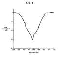
- the transmission spectrum of the Fig. 6 device is that shown in Fig. 5 .
- the spectrum (after the higher order LP 02 mode was stripped) shows a 50 nm bandwidth at the -10 dB point corresponding to 90% conversion. This is a tenfold increase in bandwidth.
- the design of wideband long-period gratings for different wavelengths and conversion between different modes is described in Part III, below.
- gratings that couple light from the fundamental mode to a higher-order spatial mode (say, the LP 11 or LP 02 mode) are useful in dispersion compensating modules that use the higher-order mode of a fiber close to cutoff to provide high negative dispersions.
- An optical communications system employing such a dispersion compensation module is schematically shown in Fig. 7 .
- a single-mode transmission fiber 70 (which carries the dispersed pulses) is spliced to a mode-converting grating 71 that converts a large fraction (> 90%) of the light into the higher order (denoted by LP lm ) mode.
- the grating is spliced to a dispersion-compensating fiber (DCF) 72 which provides a high negative dispersion and thus compresses the pulses.
- the DCF is further spliced to another mode-coupling grating 73 that couples light from the higher-order mode back to the fundamental mode.
- a single-mode fiber 74 spliced to the grating transmits the compressed pulses either to the receiver 75 or to the next span of a fiber optic system.
- FIG. 8 schematically illustrates an optical communications system comprising a transmitter 80, a receiver 83 and an alternating sequence of optical amplifiers 81 and extended lengths of optical fiber 82 disposed between the transmitter and receiver.
- the amplifiers 81 particularly rare earth fiber amplifiers, exhibit gain which is a function of wavelength.
- a filter comprising a wide band long period grating as described herein, is disposed in series with one or more of the rare earth fibers to produce a more uniform spectral response.
- the advantage of the wideband filter is that it can equalize gain over a wide bandwidth corresponding to a multiplicity of communications channels.
- Fig. 9 illustrates a preferred optical amplifier 81 for use in the communications system of Fig. 8 .
- the amplifier comprises a pair of rare earth doped fibers 91, 93 with a 92 disposed between them.
- the filter comprises a wideband long period grating as described herein.
- the grating has a strength and bandwidth chosen to flatten the spectral output of the amplifier.
- ⁇ p (n 1 - n 2 ) ⁇
- n 1 is the effective index of the first mode
- n 2 is the effective index of the second mode
- A is the periodicity of the grating.
- ⁇ n g is close to zero at ⁇ p and changes sign on either side of the zero point. This can be done using the modeling tools set forth by T. Lenahan, "Calculation of modes in an optical fiber using the finite element method and EISPACK", Bell System Technical Journal, Vol. 62, p. 2663-2694, et seq. (1983 ).
- the first step in our design procedure is to start with a standard step-index fiber having a core containing 18% germanium (and hence ⁇ ⁇ 1.8%) and a core diameter of - 9 microns. This is a starting point for a design that allows the propagation of three modes. The choice of these parameters is based upon a simple calculation of waveguide parameters and allows ease of fabrication.
Landscapes
- Physics & Mathematics (AREA)
- Optics & Photonics (AREA)
- General Physics & Mathematics (AREA)
- Engineering & Computer Science (AREA)
- Electromagnetism (AREA)
- Microelectronics & Electronic Packaging (AREA)
- Plasma & Fusion (AREA)
- Lasers (AREA)
- Optical Communication System (AREA)
- Optical Modulation, Optical Deflection, Nonlinear Optics, Optical Demodulation, Optical Logic Elements (AREA)
- Light Guides In General And Applications Therefor (AREA)
- Optical Fibers, Optical Fiber Cores, And Optical Fiber Bundles (AREA)
Claims (5)
- Eine Gittervorrichtung mit langer Periode, bestimmt für den Betrieb bei einer Betriebswellenlänge λ von annähernd 1,55 µm, und für die Bereitstellung eines Übertragungswellenlängenbands und einer Spitzenkopplungswellenlänge λp, bei welcher die Kopplung zwischen zwei optischen Modi mit gleicher Ausbreitungsrichtung erfolgt, umfassend eine Teilstrecke eines optischen Wellenleiters (10) mit einer Ummantelung (12), welche einen inneren Kern (11) umhüllt, wobei in der besagten Teilstrecke des optischen Wellenleiters (10) ein Gitter (13) mit langer Periode definiert ist, dessen Periode A größer als 10 λ ist, wobei der Wellenleiter vier konzentrische Bereiche umfasst, wobei der erste Bereich der innere Kern mit einem Radius von 4,3 µm ist, wobei die Ummantelung eine Verbundummantelung ist und den zweiten konzentrischen Bereich, welcher an den Kern angrenzt und eine Dicke von 3,15 µm aufweist, den dritten konzentrischen Bereich, welcher an den zweiten konzentrischen Bereich angrenzt und eine Dicke von 5,6 µm aufweist, und den vierten konzentrischen Bereich, welcher an den dritten konzentrischen Bereich angrenzt und sich ausdehnt, um einen nominalen Außendurchmesser von 125 µm bereitzustellen, umfasst, wobei, im Verhältnis zum Brechungsindex des zweiten Bereichs, der Index des Kerns um 1,8 % höher ist, der Index des dritten Bereichs um 0,4 % höher ist, und der Index des vierten Bereichs derselbe ist wie der Index des zweiten Bereichs, wobei das Gitter mit langer Periode derart ausgelegt ist, dass die Eigenfunktion dNdλp ein Extremum aufweist, welches bei circa 1,55 µm liegt.
- Die Gittervorrichtung nach Anspruch 1, wobei die besagten zwei optischen Modi mit gleicher Ausbreitungsrichtung jeweils effektive Gruppenindizes n1 und n2 bei der Betriebswellenlänge λ aufweisen und die Differenz Δng zwischen den beiden Gruppenindizes niedriger als 0,0025 ist.
- Die Gittervorrichtung nach Anspruch 1 oder Anspruch 2, wobei das besagte Gitter mit langer Periode bei einer mittleren Wellenlänge von 1,525 µm um einen Mikrometer gechirpt ist, um eine Übertragungsbandweite von 100 nm bereitzustellen.
- Die Gittervorrichtung nach Anspruch 3, wobei die besagten Modi der LP01-Modus und der LP02-Modus sind.
- Ein optisches Kommunikationssystem (81) mit einem optischen Signalsender (80), einem optischen Empfänger (83), einem optischen Pfad mit optischer Faser (82) und dazwischen angeordneten optischen Verstärkern (81), wobei die besagten optischen Verstärker (81) eine wellenlängenabhängige Verstärkung aufweisen, wobei der besagte optische Pfad mindestens einen Filter (92) umfasst, um die spektrale Abhängigkeit der besagten Verstärker (81) mit einer breitbandigen Gittervorrichtung mit langer Periode nach einem beliebigen der Ansprüche 1 bis 4 zu reduzieren.
Applications Claiming Priority (2)
| Application Number | Priority Date | Filing Date | Title |
|---|---|---|---|
| US53236 | 1998-04-01 | ||
| US09/053,236 US6084996A (en) | 1998-04-01 | 1998-04-01 | Broadband long-period gratings |
Publications (3)
| Publication Number | Publication Date |
|---|---|
| EP0947864A2 EP0947864A2 (de) | 1999-10-06 |
| EP0947864A3 EP0947864A3 (de) | 2000-06-21 |
| EP0947864B1 true EP0947864B1 (de) | 2010-09-15 |
Family
ID=21982820
Family Applications (1)
| Application Number | Title | Priority Date | Filing Date |
|---|---|---|---|
| EP99302188A Expired - Lifetime EP0947864B1 (de) | 1998-04-01 | 1999-03-22 | Breitbandiges Gitter mit langer Periode |
Country Status (4)
| Country | Link |
|---|---|
| US (1) | US6084996A (de) |
| EP (1) | EP0947864B1 (de) |
| JP (1) | JPH11344620A (de) |
| DE (1) | DE69942758D1 (de) |
Families Citing this family (15)
| Publication number | Priority date | Publication date | Assignee | Title |
|---|---|---|---|---|
| US6339665B1 (en) * | 1998-03-26 | 2002-01-15 | Lasercomm Inc. | Apparatus and method for compensation of chromatic dispersion in optical fibers |
| JP3149921B2 (ja) * | 1998-05-18 | 2001-03-26 | 住友電気工業株式会社 | 光損失フィルタおよびその製造方法 |
| JP2001230477A (ja) | 2000-02-16 | 2001-08-24 | Nec Corp | 光増幅装置 |
| JP2001267665A (ja) * | 2000-03-16 | 2001-09-28 | Sumitomo Electric Ind Ltd | 光増幅用光ファイバ、光ファイバ増幅器および光ファイバレーザ発振器 |
| US6845194B2 (en) * | 2001-06-27 | 2005-01-18 | Furukawa Electric North America Inc. | Optical bandpass filter using long period gratings |
| JP4138557B2 (ja) | 2003-03-31 | 2008-08-27 | 富士通株式会社 | 波長分散補償制御システム |
| KR100628472B1 (ko) * | 2004-05-24 | 2006-09-26 | 한국과학기술연구원 | few mode 광섬유 격자를 이용한 라만 또는 어븀 광섬유 레이저와 이를 이용한 온도와 스트레인 동시 측정을 위한 장거리 센서 |
| DE102004062849A1 (de) * | 2004-12-27 | 2006-07-06 | Carl Baasel Lasertechnik Gmbh & Co. Kg | Laseraktive optische Faser für einen Faserlaser oder einen faseroptischen Verstärker |
| US20060233554A1 (en) * | 2005-04-14 | 2006-10-19 | Siddharth Ramachandran | Optical fiber systems for delivering short high power pulses |
| KR100730300B1 (ko) | 2005-09-14 | 2007-06-19 | 한국전자통신연구원 | 역방향 클래딩모드 결합을 이용한 광신호 검출장치 |
| US7228029B1 (en) * | 2005-09-20 | 2007-06-05 | Furukawa Electric North America Inc. | Short pulse lasers using large mode area fibers and higher order modes |
| KR100798914B1 (ko) | 2005-09-28 | 2008-01-29 | 한국전자통신연구원 | 광섬유를 이용한 파장선별적 광집속장치 및 이를 이용한광모듈 |
| JP2007094350A (ja) | 2005-09-28 | 2007-04-12 | Korea Electronics Telecommun | 光ファイバを利用した波長選別式光集束装置及びそれを利用した光モジュール |
| CN101688944B (zh) * | 2007-02-05 | 2016-03-30 | Ofs菲特尔有限责任公司 | 在与信号模基本相同的高阶模下泵浦 |
| JP5215699B2 (ja) * | 2008-03-25 | 2013-06-19 | 日本電信電話株式会社 | フォトニック結晶ファイバ |
Family Cites Families (5)
| Publication number | Priority date | Publication date | Assignee | Title |
|---|---|---|---|---|
| US5104209A (en) * | 1991-02-19 | 1992-04-14 | Her Majesty The Queen In Right Of Canada, As Represented By The Minister Of Communications | Method of creating an index grating in an optical fiber and a mode converter using the index grating |
| US5703978A (en) * | 1995-10-04 | 1997-12-30 | Lucent Technologies Inc. | Temperature insensitive long-period fiber grating devices |
| US5764829A (en) * | 1996-02-26 | 1998-06-09 | Lucent Technologies Inc. | Optical signal shaping device for complex spectral shaping applications |
| US5757540A (en) * | 1996-09-06 | 1998-05-26 | Lucent Technologies Inc. | Long-period fiber grating devices packaged for temperature stability |
| US5953471A (en) * | 1997-07-01 | 1999-09-14 | Lucent Technologies, Inc. | Optical communication system having short period reflective Bragg gratings |
-
1998
- 1998-04-01 US US09/053,236 patent/US6084996A/en not_active Expired - Lifetime
-
1999
- 1999-03-22 DE DE69942758T patent/DE69942758D1/de not_active Expired - Lifetime
- 1999-03-22 EP EP99302188A patent/EP0947864B1/de not_active Expired - Lifetime
- 1999-04-01 JP JP11094603A patent/JPH11344620A/ja active Pending
Also Published As
| Publication number | Publication date |
|---|---|
| DE69942758D1 (de) | 2010-10-28 |
| JPH11344620A (ja) | 1999-12-14 |
| US6084996A (en) | 2000-07-04 |
| EP0947864A2 (de) | 1999-10-06 |
| EP0947864A3 (de) | 2000-06-21 |
Similar Documents
| Publication | Publication Date | Title |
|---|---|---|
| US5757540A (en) | Long-period fiber grating devices packaged for temperature stability | |
| EP0793123B1 (de) | Einrichtung zur optischen Signalformung für Anwendungen bei komplexen Spektral-formen | |
| Stegall et al. | Dispersion control with use of long-period fiber gratings | |
| EP0767391B1 (de) | Temperaturunempfindliche Fasergittervorrichtungen mit grosser Gitterperiode | |
| Vengsarkar et al. | Long-period fiber gratings as band-rejection filters | |
| EP0947864B1 (de) | Breitbandiges Gitter mit langer Periode | |
| US6289699B1 (en) | Wavelength selective optical couplers | |
| US6169837B1 (en) | Dispersion-flattened optical fiber | |
| EP0807271B1 (de) | Breitbandgitter | |
| EP0866574B1 (de) | Dispersionskompensierte optische Faser und ein entsprechendes Übertragungssystem | |
| US20020105727A1 (en) | Fabricating optical waveguide gratings | |
| EP0668520A2 (de) | Dispersionskompensierten optischen Wellenleiter enthaltender Gegenstand | |
| US6266463B1 (en) | Chirped optical fibre grating | |
| EP0831345A2 (de) | Faseroptisches Gitter | |
| EP0598554A1 (de) | Optische Faser mit negativer Dispersion | |
| US6317538B1 (en) | Optical waveguide device and optical device having long-period grating | |
| US6400868B1 (en) | Photosensitive optical fiber for a bragg grating filter, a method of fabricating said fiber, and a chromatic dispersion and chromatic dispersion slope compensator including a fiber of this kind | |
| EP1049275B1 (de) | Dispersionskompensierungseinheit | |
| KR20010068798A (ko) | 다중 클래딩 구조를 이용하여 온도 보상된 장주기 광섬유격자 필터 | |
| US20070147754A1 (en) | Optical fiber | |
| EP1421418B1 (de) | Erbiumdotierte optische verstärkungsfaser mit hoher absorption | |
| US6529671B2 (en) | Passively compensated optical fibers | |
| EP1333299B1 (de) | Optische Faser und geneigtes Fasergitter | |
| Riant et al. | Gain equalization with optimized slanted Bragg grating on adapted fibre for multichannel long-haul submarine transmission | |
| Quetel et al. | Chromatic dispersion compensation by apodised Bragg gratings within controlled tapered fibers |
Legal Events
| Date | Code | Title | Description |
|---|---|---|---|
| PUAI | Public reference made under article 153(3) epc to a published international application that has entered the european phase |
Free format text: ORIGINAL CODE: 0009012 |
|
| AK | Designated contracting states |
Kind code of ref document: A2 Designated state(s): DE FR GB IT |
|
| AX | Request for extension of the european patent |
Free format text: AL;LT;LV;MK;RO;SI |
|
| PUAL | Search report despatched |
Free format text: ORIGINAL CODE: 0009013 |
|
| RIC1 | Information provided on ipc code assigned before grant |
Free format text: 7G 02B 6/293 A, 7G 02B 6/124 B, 7H 04B 10/18 B, 7H 01S 3/06 B |
|
| AK | Designated contracting states |
Kind code of ref document: A3 Designated state(s): AT BE CH CY DE DK ES FI FR GB GR IE IT LI LU MC NL PT SE |
|
| AX | Request for extension of the european patent |
Free format text: AL;LT;LV;MK;RO;SI |
|
| 17P | Request for examination filed |
Effective date: 20001207 |
|
| AKX | Designation fees paid |
Free format text: DE FR GB IT |
|
| 17Q | First examination report despatched |
Effective date: 20050202 |
|
| RAP3 | Party data changed (applicant data changed or rights of an application transferred) |
Owner name: LUCENT TECHNOLOGIES INC. |
|
| GRAP | Despatch of communication of intention to grant a patent |
Free format text: ORIGINAL CODE: EPIDOSNIGR1 |
|
| GRAS | Grant fee paid |
Free format text: ORIGINAL CODE: EPIDOSNIGR3 |
|
| GRAA | (expected) grant |
Free format text: ORIGINAL CODE: 0009210 |
|
| AK | Designated contracting states |
Kind code of ref document: B1 Designated state(s): DE FR GB IT |
|
| REG | Reference to a national code |
Ref country code: GB Ref legal event code: FG4D |
|
| REF | Corresponds to: |
Ref document number: 69942758 Country of ref document: DE Date of ref document: 20101028 Kind code of ref document: P |
|
| PLBE | No opposition filed within time limit |
Free format text: ORIGINAL CODE: 0009261 |
|
| STAA | Information on the status of an ep patent application or granted ep patent |
Free format text: STATUS: NO OPPOSITION FILED WITHIN TIME LIMIT |
|
| 26N | No opposition filed |
Effective date: 20110616 |
|
| REG | Reference to a national code |
Ref country code: DE Ref legal event code: R097 Ref document number: 69942758 Country of ref document: DE Effective date: 20110616 |
|
| REG | Reference to a national code |
Ref country code: GB Ref legal event code: 732E Free format text: REGISTERED BETWEEN 20131121 AND 20131127 |
|
| REG | Reference to a national code |
Ref country code: FR Ref legal event code: CD Owner name: ALCATEL-LUCENT USA INC. Effective date: 20131122 |
|
| REG | Reference to a national code |
Ref country code: FR Ref legal event code: GC Effective date: 20140410 |
|
| REG | Reference to a national code |
Ref country code: FR Ref legal event code: RG Effective date: 20141015 |
|
| REG | Reference to a national code |
Ref country code: FR Ref legal event code: PLFP Year of fee payment: 17 |
|
| REG | Reference to a national code |
Ref country code: FR Ref legal event code: PLFP Year of fee payment: 18 |
|
| PGFP | Annual fee paid to national office [announced via postgrant information from national office to epo] |
Ref country code: FR Payment date: 20160321 Year of fee payment: 18 Ref country code: GB Payment date: 20160321 Year of fee payment: 18 |
|
| PGFP | Annual fee paid to national office [announced via postgrant information from national office to epo] |
Ref country code: DE Payment date: 20160330 Year of fee payment: 18 |
|
| PGFP | Annual fee paid to national office [announced via postgrant information from national office to epo] |
Ref country code: IT Payment date: 20160324 Year of fee payment: 18 |
|
| REG | Reference to a national code |
Ref country code: DE Ref legal event code: R119 Ref document number: 69942758 Country of ref document: DE |
|
| GBPC | Gb: european patent ceased through non-payment of renewal fee |
Effective date: 20170322 |
|
| REG | Reference to a national code |
Ref country code: FR Ref legal event code: ST Effective date: 20171130 |
|
| PG25 | Lapsed in a contracting state [announced via postgrant information from national office to epo] |
Ref country code: DE Free format text: LAPSE BECAUSE OF NON-PAYMENT OF DUE FEES Effective date: 20171003 Ref country code: FR Free format text: LAPSE BECAUSE OF NON-PAYMENT OF DUE FEES Effective date: 20170331 |
|
| PG25 | Lapsed in a contracting state [announced via postgrant information from national office to epo] |
Ref country code: IT Free format text: LAPSE BECAUSE OF NON-PAYMENT OF DUE FEES Effective date: 20170322 Ref country code: GB Free format text: LAPSE BECAUSE OF NON-PAYMENT OF DUE FEES Effective date: 20170322 |