EP0945874B1 - Nonvolatile semiconductor memory device - Google Patents
Nonvolatile semiconductor memory device Download PDFInfo
- Publication number
- EP0945874B1 EP0945874B1 EP99105870A EP99105870A EP0945874B1 EP 0945874 B1 EP0945874 B1 EP 0945874B1 EP 99105870 A EP99105870 A EP 99105870A EP 99105870 A EP99105870 A EP 99105870A EP 0945874 B1 EP0945874 B1 EP 0945874B1
- Authority
- EP
- European Patent Office
- Prior art keywords
- write
- data
- address
- bit
- signal
- Prior art date
- Legal status (The legal status is an assumption and is not a legal conclusion. Google has not performed a legal analysis and makes no representation as to the accuracy of the status listed.)
- Expired - Lifetime
Links
Images
Classifications
-
- G—PHYSICS
- G11—INFORMATION STORAGE
- G11C—STATIC STORES
- G11C14/00—Digital stores characterised by arrangements of cells having volatile and non-volatile storage properties for back-up when the power is down
-
- G—PHYSICS
- G11—INFORMATION STORAGE
- G11C—STATIC STORES
- G11C16/00—Erasable programmable read-only memories
- G11C16/02—Erasable programmable read-only memories electrically programmable
- G11C16/06—Auxiliary circuits, e.g. for writing into memory
- G11C16/10—Programming or data input circuits
- G11C16/14—Circuits for erasing electrically, e.g. erase voltage switching circuits
- G11C16/16—Circuits for erasing electrically, e.g. erase voltage switching circuits for erasing blocks, e.g. arrays, words, groups
-
- G—PHYSICS
- G11—INFORMATION STORAGE
- G11C—STATIC STORES
- G11C16/00—Erasable programmable read-only memories
- G11C16/02—Erasable programmable read-only memories electrically programmable
- G11C16/06—Auxiliary circuits, e.g. for writing into memory
- G11C16/10—Programming or data input circuits
Definitions
- the present invention relates to an electrically erasable and programmable nonvolatile semiconductor memory device such as an EEPROM (Electrically Erasable and Programmable Read Only Memory) and, more particularly, to a nonvolatile semiconductor memory device capable of high-speed rewrite processing.
- EEPROM Electrically Erasable and Programmable Read Only Memory
- a microcomputer incorporating an EEPROM conventionally rewrites data at an arbitrary address in the EEPROM by erasing and writing data in units of addresses.
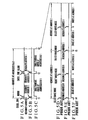
- a conventional EEPROM write operation will be explained with reference to Figs. 5D to 5F.
- Data at a plurality of addresses e.g., addresses 0 and 1 in the EEPROM can only be rewritten by two rewrite operations (one rewrite operation includes a pair of erase and write) of address 0 at time t4 and address 1 at time t5, as shown in Figs. 5D, 5E, and 5F.
- the EEPROM rewrite time is much longer than the normal machine cycle of the microcomputer, so the EEPROM rewrite time is very long in the microcomputer incorporating the conventional EEPROM.
- a nonvolatile semiconductor memory device according to the preamble part of the main claim is know from JP-A-09 180 487 and US-A-5 732 018.
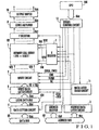
- Fig. 1 shows an EEPROM according to the first embodiment of the present invention.
- the EEPROM of the first embodiment comprises a memory cell array 1 formed by arranging a plurality of memory cells in a matrix, an address decoder 2 for outputting address selection signals SEL0 to SELF for designating one of addresses 0 to F (hexadecimal) in accordance with lower 4 bits of an 8-bit address signal input to an address bus AB, an address data latch circuit 3 for latching upper 4 bits of the 8-bit address signal input to the address bus AB, a data setting circuit 4 for, in an erase mode, inverting 8-bit data input to a data bus DB and outputting the inverted data to a local data bus LDB, and in a write mode, directly outputting 8-bit data to the local data bus LDB, and a write data latch circuit 5 for latching data output from the data setting circuit 4 via the local data bus LDB to a latch circuit at an address designated by the address selection signal SEL.
- the EEPROM further comprises a write circuit 6 for setting one of a plurality of write digit lines WB which corresponds to an address at which data "1" is written in the write data latch circuit 5, to a selection level, and an X decoder 7 for setting a write or read word line of a plurality of write digit lines WW or RW which corresponds to a page designated by a 4-bit address signal output from the address data latch circuit 3, to a selection level.
- the EEPROM further comprises a sense amplifier 8 for amplifying memory information of an 8-bit memory cell, a Y selector 9 for selecting one of a plurality of read digit lines RB in accordance with the address selection signals SEL0 to SELF and connecting the selected line to the sense amplifier 8, an output buffer 10 for externally outputting 8-bit data output from the sense amplifier 8, a data latch erase circuit 11 for clearing all data in the write data latch circuit 5 at the same time as the completion of an erase and write, and a timing control circuit 12 for generating various control signals in accordance with externally input instructions.
- a sense amplifier 8 for amplifying memory information of an 8-bit memory cell
- a Y selector 9 for selecting one of a plurality of read digit lines RB in accordance with the address selection signals SEL0 to SELF and connecting the selected line to the sense amplifier 8
- an output buffer 10 for externally outputting 8-bit data output from the sense amplifier 8
- a data latch erase circuit 11 for clearing all data in the write data latch circuit 5
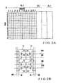
- Fig. 2A shows the schematic arrangement of the memory cell array 1 in Fig. 1.
- the EEPROM of the first embodiment is a memory capable of processing 8-bit input/output data at once.
- the memory cell array 1 is divided into eight memory blocks 20-0 to 20-7 corresponding to respective bits 0 to 7.
- the memory blocks 20-0 to 20-7 have the same arrangement.
- Each of the memory blocks 20-0 to 20-7 has a matrix of 16 (along the vertical direction corresponding to pages 0 to F; hexadecimal) ⁇ 16 (along the horizontal direction corresponding to addresses 0 to F; hexadecimal) memory cells 21.
- the memory cell array 1 has a capacity of 256 x 8 bits.
- Fig. 2B shows the detailed arrangement of the memory cell 21 in Fig. 2A.
- Fig. 2B shows the arrangement of 2 pages (along the vertical direction) ⁇ 2 addresses (along the horizontal direction) in the memory cell array 1 in Fig. 2A.
- Each memory cell 21 is made up of one memory cell transistor 22 and one n-channel MOS transistor 23.
- the control gates of the memory cell transistors 22 on respective rows corresponding to pages 0 to F are connected to the write word lines WW arranged in units of rows.
- the gates of the n-channel transistors 23 on respective rows are connected to the read word lines RW arranged in units of rows. Note that the numbers of write and read word lines WW and RW arranged in correspondence with pages 0 to F are 16 each.
- the memory cell transistors 22 on respective columns corresponding to addresses 0 to F have drains connected to the write digit lines WB arranged in units of columns, and sources connected to the drains of the n-channel MOS transistors 23 on the same columns.
- Table 1 shows the operating voltages of the write word line WW, read word line RW, write digit line WB, and read digit line RB in the erase, write, and read modes.
- the left of "/" represents a selection voltage level
- the right of "/" represents a non-selection voltage level.
- VCC is a power supply voltage of about 5 V
- VPP is a relatively high voltage of about 10 V
- V1 is 1/2 VPP
- V2 is a relatively low voltage of about 1 V.
- 0 V and the high voltage VPP are respectively applied to the control gate and drain of a memory cell transistor selected by the selected write word and digit lines out of the memory cell transistors 22 of the memory cell array 1.
- the high voltage VPP is applied to a selected one of the write word lines WW, 1/2 VPP is applied to unselected write word lines, and 0 V is applied to all the read word lines RW.
- 0 V is applied to a selected one of the write digit lines WB, and 1/2 VPP is applied to unselected write digit lines. All the read digit lines RB are set to a floating (open) state.
- the high voltage VPP and 0 V are respectively applied to the control gate and drain of a memory cell transistor selected from the memory cell transistors 22 of the memory cell array 1 by the selected write word and digit lines.
- the power supply voltage VCC is applied to a selected one of the read word lines RW, and 0 V is applied to unselected read word lines.
- An n-channel MOS transistor 23 selected by the selected read word line is turned on.
- the potential of the read digit line RB changes in accordance with the electron amount in the floating gate of the selected memory cell transistor, thereby reading out memory information of the memory cell 21.
- the address decoder 2 outputs the address selection signals SEL0 to SELF for designating one of addresses 0 to F (hexadecimal) to the write data latch circuit 5 and Y selector 9 in accordance with lower 4 bits of an 8-bit address signal input to the address bus AB from outside the EEPROM.
- the address data latch circuit 3 latches and outputs, to the X decoder, upper 4 bits of the 8-bit address signal externally input to the address bus AB.
- the data setting circuit 4 for setting data "1" in the write data latch circuit 5 inverts and outputs, to the local data bus LDB, 8-bit data externally input to the data bus DB in accordance with write/erase mode selection signals EWS0 and EWS1.
- the data setting circuit 4 directly outputs 8-bit data to the local data bus LDB.
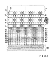
- Fig. 3 shows the detailed arrangement of the data bus DB, data setting circuit 4, and local data bus LDB shown in Fig. 1.
- the data setting circuit 4 is constituted by bit setting circuits 4-0 to 4-7 arranged in units of bits 0 to 7.
- Each of the bit setting circuits 4-0 to 4-7 is made up of an inverter 41 having an input connected to the data bus DB, an output connected to the local data bus LDB, and a control input for receiving the write/erase mode selection signal EWS0, and a buffer 42 having an input connected to the data bus DB, an output connected to the local data bus LDB, and a control input for receiving the write/erase mode selection signal EWS1.
- the bit setting circuits 4-0 to 4-7 have the same arrangement.
- the inverter 41 and buffer 42 of the data setting circuit 4-0 corresponding to bit 0 have inputs connected to bit 0 of the data bus DB, and outputs connected to bit 0 of the local data bus LDB.
- the inverter 41 and buffer 42 of the data setting circuit 4-1 corresponding to bit 1 have inputs connected to bit 1 of the data bus DB, and outputs connected to bit 1 of the local data bus LDB.
- the inverters 41 and buffers 42 of the data setting circuits 4-2, 4-3, 4-4, 4-5, 4-6, and 4-7 corresponding to bits 2, 3, 4, 5, 6, and 7 have inputs connected to bits 2, 3, 4, 5, 6, and 7 of the data bus DB, and outputs connected to bits 2, 3, 4, 5, 6, and 7 of the local data bus LDB.
- Each inverter 41 is set to an enable state by an active ("H"-level) write/erase mode selection signal EWS0 and to a disable state by an "L"-level write/erase mode selection signal EWS0.
- Each buffer 42 is set to an enable state by an active ("H"-level) write/erase mode selection signal EWS1 and to a disable state by an "L"-level write/erase mode selection signal EWS1.
- the data setting circuit 4 Inverts and outputs 8-bit data input to the data bus DB to the local data bus LDB.
- the write/erase mode selection signal EWS1 becomes active to designate the write mode, the data setting circuit 4 directly outputs 8-bit data input to the data bus DB to the local data bus LDB.
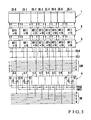
- Fig. 4 shows the detailed arrangement of the write data latch circuit 5 and write circuit 6. Fig. 4 shows only an arrangement corresponding to bit 0 out of bits 0 to 7.
- the write data latch circuits 5 are arranged in units of bits 0 to 7. As shown in Fig. 4, the write data latch circuit 5 for one bit is made up of 16 latch circuits 51 corresponding to addresses 0 to F (hexadecimal).
- each latch circuit 51 is connected to a corresponding bit of the local data bus LDB.
- the data input of each latch circuit 51 of a write data latch circuit 5 corresponding to bit 0 is connected to bit 0 of the local data bus LDB.
- each latch circuit 51 of a write data latch circuit 5 corresponding to bit 1 is connected to bit 1 of the local data bus LDB.
- the data inputs of latch circuits 51 of write data latch circuits 5 corresponding to bits 2, 3, 4, 5, 6, and 7 are respectively connected to bits 2, 3, 4, 5, 6, and 7 of the local data bus LDB.
- the clock inputs of the latch circuits 51 are respectively connected to the address selection signals SEL0 to SELF for designating corresponding addresses.
- the clock input of a latch circuit 51 corresponding to address 0 is connected to the address selection signal SEL0.
- the clock input of a latch circuit 51 corresponding to address 1 is connected to the address selection signal SEL1.
- latch circuits 51 corresponding to addresses 2, 3, 4, 5, 6, 7, 8, 9, A, B, C, D, E, and F are respectively connected to the address selection signals SEL2, SEL3, SEL4, SEL5, SEL6, SEL7, SEL8, SEL9, SELA, SELB, SELC, SELD, SELE, and SELF.
- each latch circuit 51 latches and outputs a value input to the data input. At this time, the latch circuit 51 keeps latching the data until the completion of an erase or write.
- the write circuits 6 are arranged in units of bits 0 to 7. As shown in Fig. 4, the write circuit 6 for one bit is made up of 16 level shifters 61 corresponding to addresses 0 to F (hexadecimal). The level shifters 61 constitute a voltage generation circuit.
- each level shifter 61 is connected to the output of a latch circuit 51 at a corresponding bit and address.
- the input of a level shifter 61 corresponding to bit 0 and address 0 is connected to the output of a latch circuit 51 corresponding to bit 0 and address 0.
- each level shifter 61 is connected to write and read digit lines WB and RB at a corresponding bit and address.
- the input of a level shifter 61 corresponding to bit 0 and address 0 is connected to the write and read digit lines WB and RB corresponding to bit 0 and address 0.
- the level shifter 61 sets the connected write digit line WB to a selection level.
- the value of the selection level is determined in accordance with the write/erase mode selection signals EWS0 and EWS1.
- the X decoder 7 sets one of the 16 write word lines WW corresponding to pages 0 to F (hexadecimal) or one of the read word lines RW corresponding to pages 0 to F to a selection level in accordance with a 4-bit address signal output from the address data latch circuit 3. Similar to the write circuit 6, the value of the selection level is determined in accordance with the write/erase mode selection signals EWS0 and EWS1.
- the sense amplifier 8 arranged in units of bits 0 to 7 detects and amplifies memory information of the memory cell 21.
- the Y selector 9 arranged in units of bits 0 to 7 selects one of the 16 read digit lines RB corresponding to addresses 0 to F in accordance with the address selection signals SEL0 to SELF, and connects the selected read digit line to a corresponding sense amplifier 8. For example, a Y selector 9 corresponding to bit 0 connects a selected read digit line to a sense amplifier 8 corresponding to bit 0.
- a Y selector 9 corresponding to bit 1 connects a selected read digit line to a sense amplifier 8 corresponding to bit 1.
- the output buffer 10 outputs 8-bit data output from the sense amplifiers 8 to outside the EEPROM.
- the data latch erase circuit 11 clears all data of the write data latch circuits 5 at the same time as the completion of an erase and write, i.e., sets all data of the write data latch circuits 5 to "0".
- the timing control circuit 12 generates control signals such as the simultaneous write enable signal EME for permitting a simultaneous write, the write/erase mode selection signals EWS0 and EWS1 representing the erase or write mode, and the simultaneous write start signal RUNM representing the start of a simultaneous write in accordance with an instruction input from a CPU (Central Processing Unit) 100 outside the EEPROM.
- EME simultaneous write enable signal
- EWS0 and EWS1 representing the erase or write mode
- RUNM representing the start of a simultaneous write in accordance with an instruction input from a CPU (Central Processing Unit) 100 outside the EEPROM.
- the timing control circuit 12 Upon reception of an instruction designating a simultaneous erase from the external CPU 100, the timing control circuit 12 sets the write/erase mode selection signal EWS0 to an active state ("H" level) to designate the erase mode. At the same time, the timing control circuit 12 sets the simultaneous write enable signal EME to an active state ("H" level) to designate a simultaneous write (time t1 in Fig. 5A). At this time, the write/erase mode selection signal EWS1 is kept at "L" level.
- An address signal designating address 0 of page 2 is input from outside the EEPROM to the address bus AB, and data "0" is input to all bits 0 to 7 of the data bus DB (Fig. 5B). Since the write/erase mode selection signal EWS0 is active, the inverters 41 and buffers 42 respectively change to enable and disable states in the data setting circuits 4-0 to 4-7 corresponding to bits 0 to 7.
- the data setting circuits 4-0 to 4-7 of the data setting circuit 4 invert respective bit data of the data bus DB and output them to corresponding bits of the local data bus LDB. Since data "0" has been input to all bits 0 to 7 of the data bus DB, data "1" is output to all bits 0 to 7 of the local data bus LDB.
- Each write data latch circuit 5 latches data output from the data setting circuit 4 to the local data bus LDB in a latch circuit 51 at an address designated by the address selection signal SEL. Since the address signal designating address 0 of page 2 has been input to the address bus AB, the address decoder 2 sets only the address selection signal SEL0 designating address 0 to an active state ("H"), and sets the remaining address selection signals SEL1 to SELF to "L" level.
- each latch circuit 51 corresponding to address 0 latches data "1" output to a corresponding bit of the local data bus LDB.
- an address signal designating address 1 of page 2 is externally input to the address bus AB, and data "0" is input to all bits 0 to 7 of the data bus DB (Fig. 5B).
- the data setting circuits 4-0 to 4-7 corresponding to bits 0 to 7 invert respective bits of the data bus DB and output them to corresponding bits of the local data bus LDB. Then, data "1" is output to all bits 0 to 7 of the local data bus LDB.
- the address decoder 2 Since the address signal designating address 1 of page 2 has been input to the address bus AB, the address decoder 2 sets only the address selection signal SEL1 designating address 1 to an active state ("H" level), and sets the remaining address selection signals SEL0 and SEL2 to SELF to "L" level.
- each latch circuit 51 corresponding to address 1 latches data "1" output to a corresponding bit of the local data bus LDB. In this way, in the write data latch circuits 5 corresponding to bits 0 to 7, latch circuits 51 corresponding to addresses 0 and 1 latch and output data "1". The remaining latch circuits 51 do not latch data "1" and thus output "0".
- the timing control circuit 12 externally receives an instruction designating the start of a simultaneous write.
- the timing control circuit 12 sets the simultaneous write start signal RUNM to an active state ("H" level) to designate the start of a simultaneous write (Fig. 5A).
- the write circuits 6 corresponding to bits 0 to 7 set a write digit line corresponding to an address at which an output from the write data latch circuit 5 is "1" to a selection level (high voltage VPP) out of the 16 write digit lines WB corresponding to addresses 0 to F.
- the write circuits 6 set a write digit line corresponding to an address at which an output from the write data latch circuit 5 is "0" to a non-selection level (1/2 VPP).
- write digit lines WB corresponding to addresses 0 and 1 change to a selection level. All the read digit lines RB are in a floating state.
- the X decoder 7 sets a write word line corresponding to a page designated by an address signal from the address data latch circuit 3, to a selection level (0 V) out of the 16 write word lines WW corresponding to pages 0 to F.
- the X decoder 7 sets the remaining write word lines to a non-selection level (1/2 VPP) and all the read word lines RW to 1/2 VPP.
- the data latch erase circuit 11 changes all data of the write data latch circuits 5 to "0" at the same time as the completion of an erase under the control of the timing control circuit 12.
- the timing control circuit 12 Upon reception of an instruction designating a simultaneous write from the CPU 100 outside the EEPROM, the timing control circuit 12 sets the write/erase mode selection signal EWS1 to an active state ("H" level) to designate the write mode. At the same time, the timing control circuit 12 sets the simultaneous write enable signal EME to an active state ("H" level) to designate a simultaneous write (time t2 in Fig. 5A). Note that the timing control circuit 12 keeps the write/erase mode selection signal EWS0 at "L" level.
- An address signal designating address 0 of page 2 is input from outside the EEPROM to the address bus AB, and 8-bit data to be written at address 0 of page 2 is input to the data bus DB (Fig. 5B).
- Each write data latch circuit 5 latches data output from the data setting circuit 4 to the local data bus LDB in a latch circuit 51 at an address designated by the address selection signal SEL.
- the address decoder 2 Since the address signal designating address 0 of page 2 has been input to the address bus AB, the address decoder 2 sets only the address selection signal SEL0 designating address 0 to an active state ("H"), and sets the remaining address selection signals SEL1 to SELF to "L" level. In the write data latch circuits 5 corresponding to bits 0 to 7, each latch circuit 51 corresponding to address 0 latches data output to a corresponding bit of the local data bus LDB.
- An address signal designating address 1 of page 2 is externally input to the address bus AB, and 8-bit data to be written at address 1 of page 2 is input to the data bus DB (Fig. 5B).
- the data setting circuits 4-0 to 4-7 corresponding to bits 0 to 7 directly output respective bit data of the data bus DB to corresponding bits of the local data bus LDB.
- the address decoder 2 Since the address signal designating address 1 of page 2 has been input to the address bus AB, the address decoder 2 sets only the address selection signal SEL1 designating address 1 to an active state ("H" level), and sets the remaining address selection signals SEL0 and SEL2 to SELF to "L" level.
- each latch circuit 51 corresponding to address 1 latches data output to a corresponding bit of the local data bus LDB. Then, in the write data latch circuits 5 corresponding to bits 0 to 7, each latch circuit 51 corresponding to address 0 latches data to be written at address 0, and each latch circuit 51 a corresponding to address 1 latches data to be written at address 1.
- the timing control circuit 12 externally receives an instruction designating the start of a simultaneous write.
- the timing control circuit 12 sets the simultaneous write start signal RUNM to an active state ("H" level) to designate the start of a simultaneous write (Fig. 5A).
- the write circuits 6 corresponding to bits 0 to 7 set a write digit line corresponding to an address at which an output from the write data latch circuit 5 is "1" to a selection level (0 V) out of the 16 write digit lines WB corresponding to addresses 0 to F.
- the write circuits 6 set a write digit line corresponding to an address at which an output from the write data latch circuit 5 is "0" to a non-selection level (1/2 VPP).
- each write data latch circuit 5 Since each write data latch circuit 5 has latched data to be written at addresses 0 and 1, a latch circuit 51 which latches write data "1" outputs "1", and a latch circuit 51 which latches write data "0" outputs "0". Therefore, a write digit line WB corresponding to a bit at which the value of write data is "1" changes to a selection level out of write digit lines WB corresponding to addresses 0 and 1. All the read digit lines RB are in a floating state.
- the X decoder 7 sets a write word line corresponding to a page designated by an address signal from the address data latch circuit 3, to a selection level (high voltage VPP) out of the 16 write word lines WW corresponding to pages 0 to F.
- the X decoder 7 sets the remaining write word lines to a non-selection level (1/2 VPP) and all the read word lines RW to 0 V.
- a write word line WW corresponding to page 2 changes to a selection level. Consequently, the high voltage VPP and 0 V are respectively applied to the control gate and drain of a memory cell transistor 22 of a memory cell 21 corresponding to page 2, address 0, and a bit at which the value of data to be written at address 0 is "1", out of the memory cells 21 of the memory cell array 1.
- the data latch erase circuit 11 changes all data of the write data latch circuits 5 to "0" at the same time as the completion of a write under the control of the timing control circuit 12. As described above, according to the first embodiment, data can be simultaneously rewritten with respect to memory cells 21 at a plurality of addresses.
- the rewrite time (time interval between t1 and t3) for one operation is longer than the conventional rewrite time (time interval between t4 and t5) by a time required to sequentially transferring, to the write data latch circuit 5, data corresponding to input data to a plurality of addresses.
- this transfer time is much shorter than an actual erase/write time with respect to the memory cell 21 (time required to complete an erase/write after the simultaneous write start signal RUNM becomes active).
- Data can therefore be rewritten at a plurality of addresses within almost the same time as the conventional data rewrite time for one address, thereby greatly shortening the rewrite time.
- Data is erased/written by selecting only a memory cell 21 at an address corresponding to a latch circuit 51 of the write data latch circuit 5 in which data "1" is written, whereas no data is erased/written in a memory cell 21 at an address corresponding to a latch circuit 51 in which data "0" is written. This can decrease the number of rewrite operations with respect to the memory cell 21 and increase the service life of the memory cell 21.
- a rewrite is simultaneously performed at addresses 0 and 1 of page 2. Further, a rewrite can also be simultaneously performed at three or more addresses.
- data is repeatedly written in the write data latch circuit 5 by repeatedly inputting an address signal to the address bus AB and data to the data bus DB. After data corresponding to a desired number of addresses are transferred to the write data latch circuit 5, the simultaneous write start signal RUNM is set active.
- the first embodiment has exemplified a simultaneous write in which a rewrite is simultaneously performed at a plurality of addresses, but a byte rewrite can also be performed for each address. This byte rewrite operation will be explained.
- the timing control circuit 12 Upon reception of an instruction designating a byte erase from the external CPU 100, the timing control circuit 12 sets the write/erase mode selection signal EWS0 active to designate the erase mode (t4 in Fig. 5D). At this time, the simultaneous write enable signal EME is kept at "L" level.
- An address signal designating address 0 of page 2 is input from outside the EEPROM to the address bus AB, and data "0" is input to all bits 0 to 7 of the data bus DB (Fig. 5E).
- the data setting circuit 4 Since the write/erase mode selection signal EWS0 is active, the data setting circuit 4 inverts respective bit data of the data bus DB and outputs them to corresponding bits of the local data bus LDB. In the write data latch circuits 5 corresponding to bits 0 to 7, each latch circuit 51 corresponding to address 0 latches data "1" output to a corresponding bit of the local data bus LDB.
- each write circuit 6 sets a write digit line corresponding to an address at which an output from the write data latch circuit 5 is "1" to a selection level (high voltage VPP) a predetermined time after the write/erase mode selection signal EWS0 becomes active.
- the write circuit 6 sets a write digit line corresponding to an address at which an output from the write data latch circuit 5 is "0" to a non-selection level (1/2 VPP). In this case, write digit lines WB corresponding to address 0 in bits 0 to 7 change to the selection level.
- the X decoder 7 sets a write word line corresponding to a page designated by an address signal from the address data latch circuit 3, to a selection level (0 V) a predetermined time after the write/erase mode selection signal EWS0 becomes active.
- the X decoder 7 sets the remaining write word lines to a non-selection level (1/2 VPP) and all the read word lines RW to 1/2 VPP level. In this case, a write word line WW corresponding to page 2 changes to the selection level.
- 0 V and the high voltage VPP are respectively applied to the control gates and drains of memory cell transistors 22 of memory cells 21 corresponding to bits 0 to 7, page 2, and address 0 out of the memory cells 21 of the memory cell array 1.
- data at address 0 of page 2 are erased.
- the data latch erase circuit 11 changes all data of the write data latch circuits 5 to "0" at the same time as the completion of an erase under the control of the timing control circuit 12.
- the timing control circuit 12 Upon reception of an instruction designating a byte write from the CPU 100 outside the EEPROM, the timing control circuit 12 sets the write/erase mode selection signal EWS1 active to designate the write mode (Fig. 5D). At this time, the simultaneous write enable signal EME is kept at "L" level.
- An address signal designating address 0 of page 2 is input from outside the EEPROM to the address bus AB, and 8-bit data to be written at address 0 of page 2 is input to the data bus DB (Fig. 5B).
- the data setting circuit 4 directly outputs respective bit data of the data bus DB to corresponding bits of the local data bus LDB.
- each latch circuit 51 corresponding to address 0 latches data output to a corresponding bit of the local data bus LDB.
- each write circuit 6 sets a write digit line corresponding to an address at which an output from the write data latch circuit 5 is "0" to a selection level (0 V) a predetermined time after the write/erase mode selection signal EWS1 becomes active.
- the write circuit 6 sets a write digit line corresponding to an address at which an output from the write data latch circuit 5 is "0" to a non-selection level (1/2 VPP). In this case, write digit lines WB corresponding to address 0 in bits 0 to 7 change to the selection level.
- the X decoder 7 sets a write word line corresponding to a page designated by an address signal from the address data latch circuit 3 to a selection level (high voltage VPP) a predetermined time after the write/erase mode selection signal EWS1 becomes active.
- the X decoder 7 sets the remaining write word lines to a non-selection level (1/2 VPP) and all the read word lines RW to 0 V. In this case, a write word line WW corresponding to page 2 changes to the selection level.
- the high voltage VPP and 0 V are respectively applied to the control gate and drain of a memory cell transistor 22 of a memory cell 21 corresponding to page 2, address 0, and a bit at which the value of data to be written at address 0 is "1" out of the memory cells 21 of the memory cell array 1. Consequently, data is written at address 0 of page 2.
- the data latch erase circuit 11 changes all data of the write data latch circuits 5 to "0" at the same time as the completion of a write under the control of the timing control circuit 12. In this fashion, data can be rewritten in units of bytes.
- a CPU 100 gives the EEPROM an instruction designating a read.
- a timing control circuit 12 sets a read mode selection signal RE active to designate the read mode.
- An address signal designating address 0 of page 2 is input from the CPU 100 to an address bus AB.
- An address decoder 2 sets only an address selection signal SEL0 designating address 0 to an active state ("H"), and sets remaining address selection signals SEL1 to SELF to "L" level.
- each write circuit 6 changes all write digit lines WB to 0 V, and applies a voltage V2 to read digit lines RB to perform precharge.
- an X decoder 7 sets a read word line corresponding to a page designated by an address signal from an address data latch circuit 3, to a selection level (power supply voltage VCC) out of 16 read word lines RW corresponding to pages 0 to F.
- the X decoder 7 sets the remaining read word lines to a non-selection level (0 V) and all write word lines WW to 0 V. As a result, memory information of a selected memory cell 21 is output to the read digit line RB.
- Y selectors 9 arranged in units of bits 0 to 7 connect read digit lines RB corresponding to address 0 to sense amplifiers 8 in accordance with the address selection signals SEL0 to SELF. Then, data at address 0 of page 2 is externally output via an output buffer 10.
- the CPU 100 gives the EEPROM an address signal designating address 1 of page 2 and an instruction designating a read, thereby reading out data at address 1 of page 2.
- the CPU 100 compares the data read out from address 0 of page 2 with data to be written at address 0 of page 2. Further, the CPU 100 compares the data read out from address 1 of page 2 with data to be written at address 1 of page 2.
- circuits such as the memory cell array 1 and write data latch circuits 5 are arranged in units of bits 0 to 7, and the circuit corresponding to each bit has an arrangement corresponding to addresses 0 to F.
- This layout is employed for wiring convenience, and circuits may be arranged in units of addresses 0 to F.
- the data setting means inverts input data in the erase mode, and directly outputs input data in the write mode.
- the control means outputs a start signal to select a word line by the row selection means and a digit line by the write means.
- Data can be simultaneously rewritten in memory cells at a plurality of addresses. As a result, data can be rewritten at a plurality of addresses within almost the same time as the conventional data rewrite time for one address, thereby greatly shortening the rewrite time.
- Data is erased/written by selecting only a memory cell at a bit and address corresponding to a latch circuit in which a predetermined value (e.g., "1") is written out of the latch circuits of the data latch means.
- a predetermined value e.g., "1”
- No data is erased/written in a memory cell at a bit and address corresponding to a latch circuit in which a value (e.g., "0") other than the predetermined value is written. This can decrease the number of rewrite operations with respect to the memory cell and increase the service life of the memory cell.
Description
| Write Word Line WW | Read Word Line RW | Write Digit Line WB | Read Digit Line RB | |
| Erase | 0 V/V1 | V1/V1 | VPP/V1 | Floating |
| Write | VPP/V1 | 0 V | 0 V/V1 | Floating |
| Read | 0 V | VCC/0 V | 0 V | V2 |
Claims (5)
- A nonvolatile semiconductor memory device comprising:a memory cell array (1) in which a plurality of memory cells (21) corresponding to pluralities of bits, pages, and addresses are arranged in a matrix;a plurality of word lines (WW, RW) each commonly connected to the memory cells of a corresponding page;a plurality of digit lines (WB, RB) each commonly connected to the memory cells of a corresponding bit and address;data setting means (4) for inverting input data of a plurality of bits in an erase mode and directly outputting input data in a write mode;data latch means (5) for latching data output from said data setting means in correspondence with a bit and address designated by an address signal;row selection means (7) for selecting a word line corresponding to a page designated by an address signal out of said word lines upon reception of a simultaneous write Start signal (RUNM);write means (6) for selecting a digit line in accordance with an output from said data latch means upon reception of the simultaneous write start signal; andcontrol means (12) for reading out data in accordance with an external instruction, controlling the write and read modes, and outputting the simultaneous write start signal after input data to a plurality of addresses are sequentially latched by said data latch means, characterized by further comprising designation means (100) for supplying an external instruction for designating only an erase to said control means in a data rewrite from "1" to "0".
- A device according to claim 1, wherein said data latch circuit comprises a plurality of latch circuits corresponding to bits and addresses.
- A device according to claim 2, wherein said write means selects, from said digit lines, a digit line corresponding to a bit and address indicated by a latch circuit which holds a predetermined value.
- A device according to claim 1, further comprising designation means (100) for supplying an external instruction for designating only a write to said control means in a data rewrite from "0" to "1".
- A device according to claim 1, wherein said control means outputs a write/erase mode selection signal (EWS0/EWS1), a simultaneous write signal (EME), a read mode selection signal (RE), and the simultaneous start signal to said row selection means and said write means in accordance with an external instruction.
Applications Claiming Priority (2)
| Application Number | Priority Date | Filing Date | Title |
|---|---|---|---|
| JP7554698A JP3012589B2 (en) | 1998-03-24 | 1998-03-24 | Nonvolatile semiconductor memory device |
| JP7554698 | 1998-03-24 |
Publications (3)
| Publication Number | Publication Date |
|---|---|
| EP0945874A2 EP0945874A2 (en) | 1999-09-29 |
| EP0945874A3 EP0945874A3 (en) | 2000-07-12 |
| EP0945874B1 true EP0945874B1 (en) | 2005-09-14 |
Family
ID=13579315
Family Applications (1)
| Application Number | Title | Priority Date | Filing Date |
|---|---|---|---|
| EP99105870A Expired - Lifetime EP0945874B1 (en) | 1998-03-24 | 1999-03-23 | Nonvolatile semiconductor memory device |
Country Status (7)
| Country | Link |
|---|---|
| US (1) | US6026022A (en) |
| EP (1) | EP0945874B1 (en) |
| JP (1) | JP3012589B2 (en) |
| KR (1) | KR100291633B1 (en) |
| CN (1) | CN1109348C (en) |
| DE (1) | DE69927199T2 (en) |
| MY (1) | MY117042A (en) |
Families Citing this family (8)
| Publication number | Priority date | Publication date | Assignee | Title |
|---|---|---|---|---|
| JP2003077282A (en) * | 2001-08-31 | 2003-03-14 | Fujitsu Ltd | Nonvolatile semiconductor memory |
| JP3851865B2 (en) | 2001-12-19 | 2006-11-29 | 株式会社東芝 | Semiconductor integrated circuit |
| JP3816907B2 (en) | 2003-07-04 | 2006-08-30 | Necエレクトロニクス株式会社 | Display data storage device |
| US7092288B2 (en) * | 2004-02-04 | 2006-08-15 | Atmel Corporation | Non-volatile memory array with simultaneous write and erase feature |
| CN100368990C (en) * | 2005-12-02 | 2008-02-13 | 浙江大学 | Method and device for asynchronously computing timing coutrol instruction for multi-address space |
| CN101350222B (en) * | 2007-07-16 | 2010-10-13 | 盛群半导体股份有限公司 | Apparatus for burning pagination of scrubbed and programmable ROM as well as control method thereof |
| US10395752B2 (en) * | 2017-10-11 | 2019-08-27 | Globalfoundries Inc. | Margin test for multiple-time programmable memory (MTPM) with split wordlines |
| CN112037833B (en) * | 2019-06-04 | 2023-06-06 | 华邦电子股份有限公司 | Resistive memory and data writing method thereof |
Family Cites Families (14)
| Publication number | Priority date | Publication date | Assignee | Title |
|---|---|---|---|---|
| JPS61276200A (en) * | 1985-05-31 | 1986-12-06 | Fujitsu Ltd | Writing system for programmable rom |
| JPH0736274B2 (en) * | 1985-10-08 | 1995-04-19 | 日本電気株式会社 | Read-only memory |
| US4763305A (en) * | 1985-11-27 | 1988-08-09 | Motorola, Inc. | Intelligent write in an EEPROM with data and erase check |
| JPS63251999A (en) * | 1987-04-08 | 1988-10-19 | Mitsubishi Electric Corp | Semiconductor memory device |
| JPH02146192A (en) * | 1988-11-28 | 1990-06-05 | Nec Corp | Nonvolatile eeprom |
| JP3010632B2 (en) * | 1989-02-27 | 2000-02-21 | 日本電気株式会社 | Electrically erasable and writable nonvolatile memory |
| US5363330A (en) * | 1991-01-28 | 1994-11-08 | Mitsubishi Denki Kabushiki Kaisha | Non-volatile semiconductor memory device incorporating data latch and address counter for page mode programming |
| JP3236105B2 (en) * | 1993-03-17 | 2001-12-10 | 富士通株式会社 | Nonvolatile semiconductor memory device and operation test method thereof |
| JP3373632B2 (en) * | 1993-03-31 | 2003-02-04 | 株式会社東芝 | Nonvolatile semiconductor memory device |
| JP2922116B2 (en) * | 1993-09-02 | 1999-07-19 | 株式会社東芝 | Semiconductor storage device |
| US5517453A (en) * | 1994-09-15 | 1996-05-14 | National Semiconductor Corporation | Memory with multiple erase modes |
| KR0169418B1 (en) * | 1995-10-30 | 1999-02-01 | 김광호 | Non-volatile semiconductor memory with circuit of data self conserving at the time of page erasing |
| US5777923A (en) * | 1996-06-17 | 1998-07-07 | Aplus Integrated Circuits, Inc. | Flash memory read/write controller |
| JP3789977B2 (en) * | 1996-05-10 | 2006-06-28 | 株式会社ルネサステクノロジ | Nonvolatile semiconductor memory device |
-
1998
- 1998-03-24 JP JP7554698A patent/JP3012589B2/en not_active Expired - Fee Related
-
1999
- 1999-03-18 MY MYPI99001012A patent/MY117042A/en unknown
- 1999-03-18 US US09/271,508 patent/US6026022A/en not_active Expired - Lifetime
- 1999-03-23 DE DE69927199T patent/DE69927199T2/en not_active Expired - Fee Related
- 1999-03-23 KR KR1019990009921A patent/KR100291633B1/en not_active IP Right Cessation
- 1999-03-23 EP EP99105870A patent/EP0945874B1/en not_active Expired - Lifetime
- 1999-03-24 CN CN99105594A patent/CN1109348C/en not_active Expired - Fee Related
Also Published As
| Publication number | Publication date |
|---|---|
| US6026022A (en) | 2000-02-15 |
| KR100291633B1 (en) | 2001-05-15 |
| EP0945874A2 (en) | 1999-09-29 |
| DE69927199D1 (en) | 2005-10-20 |
| CN1229995A (en) | 1999-09-29 |
| JPH11273383A (en) | 1999-10-08 |
| CN1109348C (en) | 2003-05-21 |
| KR19990078171A (en) | 1999-10-25 |
| EP0945874A3 (en) | 2000-07-12 |
| JP3012589B2 (en) | 2000-02-21 |
| DE69927199T2 (en) | 2006-06-22 |
| MY117042A (en) | 2004-04-30 |
Similar Documents
| Publication | Publication Date | Title |
|---|---|---|
| US6157573A (en) | Nonvolatile memory system, semiconductor memory, and writing method | |
| KR100476923B1 (en) | Memory devices with page buffer having dual registers and method of using the same | |
| US6009016A (en) | Nonvolatile memory system semiconductor memory and writing method | |
| KR100205240B1 (en) | Nonvolatile semiconductor memory device having a single-bit and multi-bit cell | |
| US8717833B2 (en) | Semiconductor memory device having non-volatile memory circuits in single chip | |
| US4905197A (en) | Semiconductor memory having circuitry for discharging a digit line before verifying operation | |
| EP0805454A1 (en) | Sensing circuit for reading and verifying the content of a memory cell | |
| EP0055594B1 (en) | Electrically programmable non-volatile semiconductor memory device | |
| US6477091B2 (en) | Method, apparatus, and system to enhance negative voltage switching | |
| US5214605A (en) | Automatic erasing optimization circuit for an electrically erasable and programmable semiconductor memory and method thereof | |
| US4408306A (en) | Column and row erasable EEPROM | |
| US6621743B2 (en) | Word-line driving circuit with reduced current leakage | |
| US4805151A (en) | Nonvolatile semiconductor memory device | |
| EP0311137B1 (en) | Non-volatile semiconductor memory device | |
| US5991198A (en) | Local row decoder and associated control logic for fowler-nordheim tunneling based flash memory | |
| KR950011965B1 (en) | Non-volatile semiconductor memory device | |
| EP0089364A4 (en) | Eeprom with bulk zero program capability. | |
| EP0945874B1 (en) | Nonvolatile semiconductor memory device | |
| US5617350A (en) | Flash memory system having reduced disturb and method | |
| CA1225461A (en) | One step write circuit arrangement for eeproms | |
| JPH09204783A (en) | Semiconductor nonvolatile memory | |
| US6973003B1 (en) | Memory device and method | |
| JPH11162199A (en) | Semiconductor memory | |
| JP3544731B2 (en) | Nonvolatile semiconductor memory device | |
| JP3519542B2 (en) | Semiconductor storage device |
Legal Events
| Date | Code | Title | Description |
|---|---|---|---|
| PUAI | Public reference made under article 153(3) epc to a published international application that has entered the european phase |
Free format text: ORIGINAL CODE: 0009012 |
|
| AK | Designated contracting states |
Kind code of ref document: A2 Designated state(s): DE FR GB |
|
| AX | Request for extension of the european patent |
Free format text: AL;LT;LV;MK;RO;SI |
|
| PUAL | Search report despatched |
Free format text: ORIGINAL CODE: 0009013 |
|
| AK | Designated contracting states |
Kind code of ref document: A3 Designated state(s): AT BE CH CY DE DK ES FI FR GB GR IE IT LI LU MC NL PT SE |
|
| AX | Request for extension of the european patent |
Free format text: AL;LT;LV;MK;RO;SI |
|
| RIC1 | Information provided on ipc code assigned before grant |
Free format text: 7G 11C 16/10 A, 7G 11C 16/16 B, 7G 11C 16/34 B |
|
| 17P | Request for examination filed |
Effective date: 20000605 |
|
| AKX | Designation fees paid |
Free format text: DE FR GB |
|
| RAP1 | Party data changed (applicant data changed or rights of an application transferred) |
Owner name: NEC ELECTRONICS CORPORATION |
|
| 17Q | First examination report despatched |
Effective date: 20040804 |
|
| GRAP | Despatch of communication of intention to grant a patent |
Free format text: ORIGINAL CODE: EPIDOSNIGR1 |
|
| GRAS | Grant fee paid |
Free format text: ORIGINAL CODE: EPIDOSNIGR3 |
|
| GRAA | (expected) grant |
Free format text: ORIGINAL CODE: 0009210 |
|
| AK | Designated contracting states |
Kind code of ref document: B1 Designated state(s): DE FR GB |
|
| REG | Reference to a national code |
Ref country code: GB Ref legal event code: FG4D |
|
| REF | Corresponds to: |
Ref document number: 69927199 Country of ref document: DE Date of ref document: 20051020 Kind code of ref document: P |
|
| ET | Fr: translation filed | ||
| PLBE | No opposition filed within time limit |
Free format text: ORIGINAL CODE: 0009261 |
|
| STAA | Information on the status of an ep patent application or granted ep patent |
Free format text: STATUS: NO OPPOSITION FILED WITHIN TIME LIMIT |
|
| 26N | No opposition filed |
Effective date: 20060615 |
|
| PGFP | Annual fee paid to national office [announced via postgrant information from national office to epo] |
Ref country code: GB Payment date: 20080326 Year of fee payment: 10 |
|
| PGFP | Annual fee paid to national office [announced via postgrant information from national office to epo] |
Ref country code: FR Payment date: 20080311 Year of fee payment: 10 Ref country code: DE Payment date: 20080407 Year of fee payment: 10 |
|
| GBPC | Gb: european patent ceased through non-payment of renewal fee |
Effective date: 20090323 |
|
| REG | Reference to a national code |
Ref country code: FR Ref legal event code: ST Effective date: 20091130 |
|
| PG25 | Lapsed in a contracting state [announced via postgrant information from national office to epo] |
Ref country code: DE Free format text: LAPSE BECAUSE OF NON-PAYMENT OF DUE FEES Effective date: 20091001 |
|
| PG25 | Lapsed in a contracting state [announced via postgrant information from national office to epo] |
Ref country code: GB Free format text: LAPSE BECAUSE OF NON-PAYMENT OF DUE FEES Effective date: 20090323 Ref country code: FR Free format text: LAPSE BECAUSE OF NON-PAYMENT OF DUE FEES Effective date: 20091123 |