EP0943390A2 - Multi-laser combustion surface treatment - Google Patents
Multi-laser combustion surface treatment Download PDFInfo
- Publication number
- EP0943390A2 EP0943390A2 EP99102747A EP99102747A EP0943390A2 EP 0943390 A2 EP0943390 A2 EP 0943390A2 EP 99102747 A EP99102747 A EP 99102747A EP 99102747 A EP99102747 A EP 99102747A EP 0943390 A2 EP0943390 A2 EP 0943390A2
- Authority
- EP
- European Patent Office
- Prior art keywords
- laser
- pulses
- pulse
- beams
- sub
- Prior art date
- Legal status (The legal status is an assumption and is not a legal conclusion. Google has not performed a legal analysis and makes no representation as to the accuracy of the status listed.)
- Withdrawn
Links
Images


Classifications
-
- H—ELECTRICITY
- H01—ELECTRIC ELEMENTS
- H01S—DEVICES USING THE PROCESS OF LIGHT AMPLIFICATION BY STIMULATED EMISSION OF RADIATION [LASER] TO AMPLIFY OR GENERATE LIGHT; DEVICES USING STIMULATED EMISSION OF ELECTROMAGNETIC RADIATION IN WAVE RANGES OTHER THAN OPTICAL
- H01S3/00—Lasers, i.e. devices using stimulated emission of electromagnetic radiation in the infrared, visible or ultraviolet wave range
-
- G—PHYSICS
- G03—PHOTOGRAPHY; CINEMATOGRAPHY; ANALOGOUS TECHNIQUES USING WAVES OTHER THAN OPTICAL WAVES; ELECTROGRAPHY; HOLOGRAPHY
- G03F—PHOTOMECHANICAL PRODUCTION OF TEXTURED OR PATTERNED SURFACES, e.g. FOR PRINTING, FOR PROCESSING OF SEMICONDUCTOR DEVICES; MATERIALS THEREFOR; ORIGINALS THEREFOR; APPARATUS SPECIALLY ADAPTED THEREFOR
- G03F7/00—Photomechanical, e.g. photolithographic, production of textured or patterned surfaces, e.g. printing surfaces; Materials therefor, e.g. comprising photoresists; Apparatus specially adapted therefor
- G03F7/26—Processing photosensitive materials; Apparatus therefor
- G03F7/42—Stripping or agents therefor
-
- B—PERFORMING OPERATIONS; TRANSPORTING
- B23—MACHINE TOOLS; METAL-WORKING NOT OTHERWISE PROVIDED FOR
- B23K—SOLDERING OR UNSOLDERING; WELDING; CLADDING OR PLATING BY SOLDERING OR WELDING; CUTTING BY APPLYING HEAT LOCALLY, e.g. FLAME CUTTING; WORKING BY LASER BEAM
- B23K26/00—Working by laser beam, e.g. welding, cutting or boring
- B23K26/02—Positioning or observing the workpiece, e.g. with respect to the point of impact; Aligning, aiming or focusing the laser beam
- B23K26/06—Shaping the laser beam, e.g. by masks or multi-focusing
- B23K26/064—Shaping the laser beam, e.g. by masks or multi-focusing by means of optical elements, e.g. lenses, mirrors or prisms
-
- B—PERFORMING OPERATIONS; TRANSPORTING
- B23—MACHINE TOOLS; METAL-WORKING NOT OTHERWISE PROVIDED FOR
- B23K—SOLDERING OR UNSOLDERING; WELDING; CLADDING OR PLATING BY SOLDERING OR WELDING; CUTTING BY APPLYING HEAT LOCALLY, e.g. FLAME CUTTING; WORKING BY LASER BEAM
- B23K26/00—Working by laser beam, e.g. welding, cutting or boring
- B23K26/12—Working by laser beam, e.g. welding, cutting or boring in a special environment or atmosphere, e.g. in an enclosure
- B23K26/123—Working by laser beam, e.g. welding, cutting or boring in a special environment or atmosphere, e.g. in an enclosure in an atmosphere of particular gases
-
- H—ELECTRICITY
- H01—ELECTRIC ELEMENTS
- H01S—DEVICES USING THE PROCESS OF LIGHT AMPLIFICATION BY STIMULATED EMISSION OF RADIATION [LASER] TO AMPLIFY OR GENERATE LIGHT; DEVICES USING STIMULATED EMISSION OF ELECTROMAGNETIC RADIATION IN WAVE RANGES OTHER THAN OPTICAL
- H01S3/00—Lasers, i.e. devices using stimulated emission of electromagnetic radiation in the infrared, visible or ultraviolet wave range
- H01S3/10—Controlling the intensity, frequency, phase, polarisation or direction of the emitted radiation, e.g. switching, gating, modulating or demodulating
- H01S3/10038—Amplitude control
- H01S3/10046—Pulse repetition rate control
-
- H—ELECTRICITY
- H01—ELECTRIC ELEMENTS
- H01S—DEVICES USING THE PROCESS OF LIGHT AMPLIFICATION BY STIMULATED EMISSION OF RADIATION [LASER] TO AMPLIFY OR GENERATE LIGHT; DEVICES USING STIMULATED EMISSION OF ELECTROMAGNETIC RADIATION IN WAVE RANGES OTHER THAN OPTICAL
- H01S3/00—Lasers, i.e. devices using stimulated emission of electromagnetic radiation in the infrared, visible or ultraviolet wave range
- H01S3/23—Arrangements of two or more lasers not provided for in groups H01S3/02 - H01S3/22, e.g. tandem arrangements of separate active media
- H01S3/2383—Parallel arrangements
Definitions
- the present invention relates to laser surface treatments,, particularly to method and apparatus for the generation of laser beams, which permit high throughout and damage-free UV laser removal of foreign materials, as photoresists, particles and the like, from the surfaces of substrates, such as, e.g., semiconductor wafers in various production stages, and to surface treatments wherein said laser beams are generated by the aforesaid method and apparatus..
- Utilizing only the wet stripping method is not a perfect solution, as it cannot completely strip photoresist after tough processes that change the chemical and physical properties of the photoresist in such a way that makes its removal very difficult.
- Such processes include, e.g., High Dose Implantation (HDI), reactive Ion Etching (RIE), deep UV curing and high temperatures post-bake. After HDI or RIE, the sidewalls of the implanted patterns or of the etched walls are the most difficult to remove.
- the wet method has some other problems: the strength of the stripping solution changes with time, the accumulated contamination in the solution can be a source of particles which adversely affect the performance of the wafter, the corrosive and toxic content of stripping chemicals imposes high handling and disposal costs, and liquid phase surface tension and mass transport tend to make photoresist removal uneven and difficult.
- the dry method also suffers from some major drawbacks, especially from metallic and particulate contamination, damage due to plasma - charges, currents, electric fields and plasma-induced UV radiation, as well as temperature-induced damage, and, especially, incomplete removal.
- the photoresist suffers from chemical and physical changes which harden it, and this makes the stripping processes of the prior art extremely difficult to carry out.
- a plurality of sequential steps, involving wet and dry processes, are needed to completely remove the photoresist.
- UV ashers are sold, e.g. by Hitachi, Japan (UA-3150A)
- dry chemical ashers are also available, e.g., by Fusion Semiconductor Systems, U.S.A., which utilize nitrous oxide and ozone to remove the photoresist by chemical ashing
- microwave plasma ashing is also effected, e.g., as in the UNA-200 Asher (ULVAC Japan Ltd.).
- plasma photoresist removal is employed and is commercially available. e.g., as in the Aspen apparatus (Mattson Technology, U.S.A.), and in the AURA 200 (GASONICS IPC, U.S.A.).
- photoresist removal has been achieved by ablation, using laser UV radiation, in an oxidizing environment, as described in U.S. Patent No. 5,114,834.
- the ablation process is caused by strong absorption of the laser pulse energy by the photoresist.
- the process is a localized ejection of the photoresist layer to the ambient gas, associated with a blast wave due to chemical bonds breaking in the photoresist and instant heating.
- the partly gasified and partly fragmented photoresist is blown upwards away from the surface, and instantly heats the ambient gas.
- Fast combustion flash of the ablation products occurs, after each laser pulse,, due to the photochemical reaction of the UV laser radiation and the process gases, which may also be due to the blast wave.
- the main essence of the process is laser ablation with combustion flash of the ablated photoresist, which occurs in a reactive gas flowing through an irradiation zone.
- the combination of laser radiation and fast combustion provides instantaneous lowering of the ablation threshold of hard parts of the photoresist (side walls).
- the combusted ablation products are then removed by vacuum suction, or by gas sweeping, leaving a completely clean surface.
- U.S. 5,114,834 provides an important novel process, it still does not provide a high throughput, which is industrially convenient, viz. an industrially acceptable number of wafers that can be stripped during a given time.
- the laser stripping throughput is determined by the stripping rate or by the number of laser pulses needed for providing complete stripping of a unit area of the photoresist per unit of time.
- U.S. Patent No. 5,114,834 defines the process window of laser stripping, and indicates that there are certain energy fluence levels of the laser pulse which may damage the wafer being treated. So far, however, the art has failed to provide a method which conveniently permits to utilize the energy of an excimer laser in a way that allows to increase the fluence damage threshold defined in U.S. Patent 5,114,834, without incurring the risk of damaging the surface of the object being treated.
- the types of damage due to laser energy include thermal damages, such as ripples due in particular to difference in expansion coefficients, e.g., SiO 2 /Si (implanted) and TiN/Al interfaces and related to the fatigue phenomena, aluminum or silicon melting, as well as radiation (ionization) damages, e.g., slight color changes due to small changes in the crystalline structure at SiO 2 /Si interface (implanted).
- thermal damages such as ripples due in particular to difference in expansion coefficients, e.g., SiO 2 /Si (implanted) and TiN/Al interfaces and related to the fatigue phenomena, aluminum or silicon melting, as well as radiation (ionization) damages, e.g., slight color changes due to small changes in the crystalline structure at SiO 2 /Si interface (implanted).
- WO 97/17164 (PCT/IL/00139), the entire content of which is incorporated herein by reference, discloses a method of damage-free laser surface treatment by extending a laser pulse in time and supplying the same pulse energy to a treated surface during a longer period of time.
- the pulse extension is carried out by optical means, viz. by means of a Passive Optical Pulse Extender, hereinafter "POPE".
- POPE Passive Optical Pulse Extender
- Any high average power industrial UV-Laser has a high pulse frequency f ⁇ 200-250 Hz,, low pulse energy E ⁇ 0.5 J and constant pulse length.
- a Passive Optical Pulse Extender (POPE) does increase the duration of laser pulse while not being able to change (regulate) it, since optical delays are fixed for any given case. Therefore, a combination of any commercial high average power UV-Laser + POPE does not possess the second, third and fourth of the above-mentioned features needed for providing high (optimal) throughput.
- a variable pulse extension permits to find the approximate optimal fluence values for different types of photoresist: F ph1 opt, F ph2 opt, owing, F phi opt, owing where F phi opt is the fluence for the i-th type of photoresist.
- F phi opt requires its pulse extension.
- the implementation of a number of pulse extensions needs the continuous changing of time intervals between subpulses produced in optical pulse extenders for pulse extension (see the cited WO 97/17164).
- changing pulse extension would provide both a damage-free and an optimal Multi-Laser Combustion (MLC) surface treatment.
- MLC Multi-Laser Combustion
- the optical pulse extender has constant optical delays, and therefore cannot provide a controlled pulse extension, as well as an optimal MLC surface treatment.
- the fluences required for laser removal of foreign materials can be so high that the laser pulse duration must be extended many times to avoid damage of the treated surface.
- the combination of high power laser with optical pulse extension is not sufficient in many cases, because it cannot provide a sufficiently low pulse frequency and controlled pulse extension, and, whenever a large pulse extension is required, very high losses of pulse energy occur in the passage of the pulse through the elements of the optical extender.
- Control of the pulse extension is required, because it is necessary to provide in each case an appropriate fluence process window to avoid thermal, damage of the treated substrate. Different types of photoresists have different optimal fluence values and each of these requires a different pulse extension. Therefore, controlled pulse extension provides a MLC surface treatment that has an optimal throughput and avoids substrate damage.
- laser active medium is meant a gas or a solid which, after excitement by discharge or by flash lamp, is capable of generating a laser beam, if a resonator is provided.
- both low pulse energy and high pulse frequency lead to a lowering of throughput, due to their unfavorable influence on the efficiency of the optical line.
- Low pulse energy can provide high optimal values of working fluence only on small areas of laser beam impact. It decreases the efficiency of fluence homogenization on a wafer.
- high pulse frequency is not acceptable for dry laser chemical stripping, as hereinbefore explained, and requires a fitting dividing by optical means. As has been said, reduction of the pulse frequency by optical means also causes a significant laser energy loss. Therefore, both these factors sharply deteriorate the efficiency of the optical line.
- the method for the production of laser beams for surface treatments comprises generating and emitting a plurality of laser beams having electronically synchronized pulses with electronically controlled delays, unifying said beams to a single beam and optically splitting every laser pulse into a number of sub-pulses with constant optical delays.
- the said electronic synchronization is achieved by synchronizing the triggering of the pumping means with electronically controlled delays.
- the control of said triggering is well known to skilled persons, and can be easily accomplished by them.
- the laser beams may be optically split before or after they have been unified.
- the method may comprise modifying near or far fields of the beam, when it is generated, e.g., by expanding it and/or homogenizing it.
- the invention further provides an apparatus for carrying out the aforesaid method, which comprises a plurality of laser heads for generating and emitting laser beams, having means for synchronizing the pulses, and a Passive Optical Pulse Extender (POPE) for splitting each laser pulse into a plurality of sub-pulses and producing a controlled delay between successive pluralities of sub-pulses which correspond to different laser pulses.
- POPE Passive Optical Pulse Extender
- pulses when used alone, will refer to the original pulses as emitted by the laser heads.
- the pulses after splitting will be called “sub-pulses”, meaning “pulses that are obtained by splitting the pulses emitted by the laser emitters”.
- the said plurality of laser heads for generating and emitting laser beams, having means for synchronizing the pulses may constitute a single Multi-Head Laser with a number (hereinafter, "n") of electronically synchronized pumpings of its heads, or may be a plurality of "n" One-Head Lasers, electronically synchronized. Since in all cases said laser heads produce together an electronic pulse extension without essential losses, they will be designated together by the term “Active Electronic Pulse Extender” (hereinafter abbreviated as "AEPE").
- AEPE Active Electronic Pulse Extender
- AEPE Active Electronic Pulse Extension
- the method and apparatus of the invention produce a laser beam which has the aforesaid properties.
- the energy of the laser beam should be made to impact onto the wafer through an optical line having a high efficiency; whereby to effect removal of foreign materials from the wafer with high throughput and without any damage to it.
- a plurality of laser emitters with the same pulse frequency are combined to make a multi-laser system (AEPE), which, in combination with a POPE, constitutes an apparatus having a high average power and a pulse energy that are the sum of those of the individual emitters, and having the pulse frequency "f" of the said laser emitters and a controlled pulse duration, as hereinafter defined, and shape.
- AEPE multi-laser system
- the desired average power can be obtained.
- FIG. 1a schematically illustrates such an apparatus according to one embodiment thereof.
- a multi-laser emitter generally indicated at 10, comprises n heads, each indicated at 11, the number n remaining undetermined.
- the time interval between successive pulses produced by this system is the controlled electronic delay indicated by ⁇ e d.
- the various beams are unified and directed onto the POPE, schematically indicated at 12, and issue from said POPE as sub-pulses in the number of "m" for each original pulse. Between each group of "m" sub-pulses and the successive one, there is a controlled electronic delay.
- the time interval between successive sub-pulses of each group of in sub-pulses is the constant optical delay indicated by ⁇ o d, and, since there is said electronic delay, ⁇ c d > m ⁇ o d, However, this is true in the embodiment illustrated, but ⁇ c d is a controlled electronic delay, and could be equal to or less than m ⁇ o d. Parameter "m" will be determined by skilled persons in such a way as to obtain the best results.
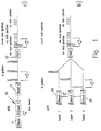
- Fig. 1b illustrates an embodiment which differs from that of Fig. 1a only in that the n laser heads are separate, each of them being embodied in a Single-Head Laser 20, and the beams separately emitted by separate resonators (instead of a single one for all, as in Fig. 1a) and directed into a common channel to the POPE, which operates as in the previous embodiment.
- Fig. 2 unlike Fig. 1b, represents every laser with its optical pulse extender, that is, laser beam unification occurs here after passing through the POPE.
- Fig. 3 is a schematic representation which generally illustrates the concept of the invention.
- the plurality of n laser heads, no matter how they are structurally realized, are generally indicated at 30 (n being 3, by way of example only, in the drawing), the unified beams are directed onto the POPE 31, which splits each pulse 32 into m sub-pulses 33 (m being 3, by way of example only, in the drawing), so that the emission of one pulse by each laser head, viz. the emission of n pulses, results in the production of n ⁇ m sub-pulses.
- Fig. 4 is provided for comparative purposes. It is assumed that a single HPL 40 is provided, and in that case, even if a POPE 41 is used, only m sub-pulses 43 result from each pulse 42 of the laser head.
- the scheme of Fig. 4 (prior art) can be compared to the general concept of the invention (Fig. 3).
- the use of a plurality of heads allows the use of lasers with a very short pulse duration (few ns) for laser stripping, and to change the fluence process window with a wide range to perform stripping in each case at the optimal fluence values.
- the duration of pulse for the excimer laser is 20-40 ns, but the duration of the solid state harmonic pulse is 3-5 ns, and is considered very short.
- the duration of each separate sub-pulse is equal to the duration of each laser pulse.
- the same average power could be obtained by means of n synchronized heads, each having the same pulse energy E and frequency f l /n (see Fig. 5).
- AEPE Multi-Head Laser System of Active Electronic Pulse Extension
- a Multi-Head Laser System In contrast to the passive optical extension (POPE), in the AEPE system, every pulse is generated by a separate laser head, which is therefore "active". Therefore, a Multi-Head Laser System simultaneously generates and extends laser pulses, controlling them and transforming them into groups of sub-pulses, forming an interval of time which may be, for example, ⁇ 0.5*10 -6 s (compared with a period of laser pulses 1/f l , which is from about 10 -3 to 10 -1 s).
- This is advantageous because the POPE introduces additional losses in the optical line.
- harmonics of solid state laser radiation with the wave length ⁇ ⁇ 200 - 250 nm have too short a pulse duration ( ⁇ ⁇ 5ns), and therefore their pulses require both electronic and optical extension, as the number of laser heads cannot be very large.
- the multi-beam system of the invention offers the option of using simultaneously two or more wavelengths of laser radiation for the removal of foreign material, in particular, different types of photoresist, from semiconductor wafers.
- Such a system is potentially much more flexible, since its influence on the stripping process efficiency is mainly due to its higher photochemical capability.
- a preferred combination of lasers for carrying out the invention is the combination of two lasers emitting beams of wavelengths 193 and 248 nm, but this is merely a preferred case and other wavelengths may be used.
- UV-Excimer lasers of main average power P av ⁇ 40 - 50 W, with a stabilized pulse energy E ⁇ 600 mJ and a laser pulse frequency f l ⁇ 50 - 100 Hz.
- Such lasers can be the main components of an industrial Multi-Head Laser System of high average power P av > 100-200 W (for a number of laser heads n ⁇ 2) at a low pulse frequency and high pulse energy, with controlled pulse duration and shape, as well.
- the AEPE according to the invention has many advantages, and in particular, it allows:
- pulse, pulse energy, pulse extension, or pulse fluence means that the pulse, pulse energy, pulse extension, or pulse fluence, as the case may be, is that of the beams as they issue from the AEPE.
- a high power laser system which has: 1- the low multiplicated pulse frequency needed for a balance between delivering the pulse energy and the process gas to a beam footprint on the treated substrate; 2 - a high multiplicated pulse energy which permits to work with a larger laser beam footprint area, which increases the efficiency of the optomechanical scanning of the treated surfaces; 3 - a high multiplicated pulse extension without essential losses of energy within the POPE; and 4 - a control duration of the multiplicated pulse, which permits to find the optimal value both for its duration and for a multiplicated pulse fluence, specifically for the MLC treatment of semiconductor wafers.
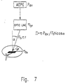
- TA block diagram of an embodiment of laser treatment of surfaces is shown in Fig. 6, on which are marked the main parameters of the separate blocks defining a throughput of the laser surface treatment process.
- Fig. 6 and to the corresponding apparatus diagram of Fig. 7, one can derive the relationship expressing the throughput as a function of P av , ⁇ , F and N at the blanket covering a treated surface by laser irradiation, where:
- ⁇ P av is the laser energy incident upon a wafer per second
- product FN is the energy required for a complete cleaning of one cm 2 of surface, for example, for a complete removal of one cm 2 of photoresist from a surface.
- Throughput rise is related, on the one side, to the efficiency of all processes, providing an article surface treatment, in particular, a foreign material removal from a surface ((1) - (4) positions), and on the other side, to an average power of pulsed laser radiation and efficiency of its delivering to a treated area of article surface ((5)-(7) positions).
- the further procedure goes through the joint optimizing function ⁇ 2 of an anisotropy of laser etching ( ⁇ , ⁇ (t)), as well as an isotropy chemical etching and the synergetically linking combustion ( ⁇ , p 1 , p 2 , p 3 , ...p n , P, T).
- ⁇ , ⁇ (t) an anisotropy of laser etching
- ⁇ , ⁇ (t) an isotropy chemical etching
- the synergetically linking combustion ⁇ , p 1 , p 2 , p 3 , ...p n , P, T.
- any new type of article e.g., new layer of photoresist
- MLC-Stripper parameters to achieve maximum throughput for this layer of photoresist, at the set level of yield.
- MLC cleaning stripping or etching (e. g., wafer planarization) technology.
- etching e. g., wafer planarization
- These MLCF surface treatments can also be applied to other articles (besides semiconductor, wafers), e. g., to flat panels and so on.
- optical line which delivers the energy of the laser to the wafer and the other components of the apparatus for the treatment of the wafer need not be described in greater detail, as they are within the knowledge and ability of skilled persons and are additionally described in the cited PCT applications.
- the beam incidence angle on the treated surface is indicated by ⁇ . It is preferably in the range from 0 to 60°.
- the beam azimuth is indicated by ⁇ , and preferably changes from pulse to pulse, or from one stage of scanning to another.
- the method and apparatus of the invention are useful in general for MLC surface foreign material removal.
- semiconductor devices such as MLC photoresist stripping of conductor wafers (VLSI/ULSI circuits), MLC surface cleaning from particulate, atomic and other contaminants, MLC surface etching. MLC dry etch planarization, and the like.
- the treated articles may be other than semiconductors, e.g. may also be Flat Panel Displays, compact disks, magnetic heads, wafers of bare silicon,
Landscapes
- Physics & Mathematics (AREA)
- Optics & Photonics (AREA)
- Engineering & Computer Science (AREA)
- Plasma & Fusion (AREA)
- Mechanical Engineering (AREA)
- Electromagnetism (AREA)
- General Physics & Mathematics (AREA)
- Cleaning Or Drying Semiconductors (AREA)
- Drying Of Semiconductors (AREA)
- Manufacturing Optical Record Carriers (AREA)
- Lasers (AREA)
- Physical Or Chemical Processes And Apparatus (AREA)
- Laser Beam Processing (AREA)
Abstract
Description
- Fig. 1a schematically illustrates the apparatus of the invention in an embodiment in which a plurality of One-Head Lasers are employed;
- Fig. 1b schematically illustrates the apparatus of the invention in an embodiment in which a Multi-Head Laser is employed;
- Fig. 2 schematically illustrates a modification of the apparatus of Fig. 1b;
- Fig. 3 is a general schematic illustration of the apparatus according to the invention;
- Fig. 4 schematically illustrates, for comparative purposes, an apparatus not according to the invention;
- Fig. 5 schematically illustrates the transition from an HPL to an AEPE;
- Fig. 6 is a block diagram of an apparatus according to an embodiment of the invention, in which η1, η2, η3, η4, η5 are the efficiencies of corresponding relay lines; ηPE is the efficiency of POPE, ηH is the efficiency of laser radiation homogenizing; ηSH is the efficiency of laser beam footprint shaping; ηdiv is the efficiency of laser beam footprint diversion; ηW is the efficiency of the process chamber window; ηG is the efficiency of process gas; and ηSC is the efficiency of laser beam footprint scanning; and
- Fig. 7 is schematic illustration of an apparatus in which
Claims (18)
- Method of MLC surface treatment by irradiation with laser beams, which comprises generating a plurality of laser beams having synchronized pulses and controlled delays, unifying said beams to a single beam and optically splitting every laser pulse into a number of sub-pulses.
- Method according to claim 1, further comprising delivering the unified beams onto the surface to be treated.
- Method according to claim 1, comprising synchronizing the pulses of the beams by synchronizing the triggering of the laser pumping means with electronically controlled delays.
- Method according to claim 1, wherein the laser beams are optically split before they are unified.
- Method according to claim 1, wherein the laser beams are optically split after they are unified.
- Method according to claim 1, wherein the optical splitting comprises constant optical delays between the sub-pulses,
- Method according to claim 1, wherein the laser sub-pulses, into which the pulses are split, have the same duration as the pulses and amplitudes corresponding to the number of sub-pulses into which each laser pulse is split.
- Method according to claim 1, wherein, if the generated laser beams are in the number of "n" and each pulse thereof is split into "m" sub-pulses, the treated surface is irradiated by a unified laser beam consisting of n×m sub-pulses and having the same frequency as said pulses and an energy equal to the sum of the separate energies of said generated laser beams.
- Method according to claim 1, further comprising homogenizing the generated beams.
- Method according to claim 1, further comprising beam diversion for shaping, scanning and orientation with respect to the treated surface.
- Method according to claim 10, wherein the scanning is implemented in a blanket manner.
- Method according to claim 10, wherein the beam orientation is such that its incidence angle α on the treated surface is in the range from 0 to 60°.
- Method according to claim 10, wherein the beam orientaton is such that its azimuth ϕ changes from pulse to pulse, or from one stage of scanning to another.
- Apparatus for the generation of a laser beam for the optimized high throughput and yield, Multi-Laser Combustion (MLC) surface treatment, which comprises;a plurality of laser heads, generating a plurality of pulsed laser beams; means for the controlled synchronization of the said laser heads;means for splitting each laser pulse into a plurality of sub-pulses with constant optical delays between them; andmeans for producing controlled electronic delays in said pluralities of said sub-pulses, which correspond to different laser pulses.
- Apparatus according to claim 14, further comprising means for homogenizing the laser beams.
- Apparatus for MLC surface treatments, comprising an apparatus according to claim 14 and further comprisingmeans for the diversion of the laser beams;means for continuous scanning of beam footprint;a process chamber with an optical window for the said laser beam, for a treated article supplied by flow of ambient process gas, moving between the said optical window and the said treated article.
- Apparatus, according to claim 14-, wherein the plurality of laser heads constitutes a plurality of lasers, each with its own resonator.
- Apparatus according to claim 14, wherein the plurality of laser heads constitutes a single multi-head laser with one resonator.
Applications Claiming Priority (2)
| Application Number | Priority Date | Filing Date | Title |
|---|---|---|---|
| IL12341698A IL123416A0 (en) | 1998-02-23 | 1998-02-23 | Multi laser surface treatment in ambient fast flowing photoreactive gases |
| IL12341698 | 1998-02-23 |
Publications (2)
| Publication Number | Publication Date |
|---|---|
| EP0943390A2 true EP0943390A2 (en) | 1999-09-22 |
| EP0943390A3 EP0943390A3 (en) | 2004-05-06 |
Family
ID=11071260
Family Applications (1)
| Application Number | Title | Priority Date | Filing Date |
|---|---|---|---|
| EP99102747A Withdrawn EP0943390A3 (en) | 1998-02-23 | 1999-02-22 | Multi-laser combustion surface treatment |
Country Status (5)
| Country | Link |
|---|---|
| US (1) | US6215099B1 (en) |
| EP (1) | EP0943390A3 (en) |
| JP (1) | JPH11317385A (en) |
| KR (1) | KR19990072815A (en) |
| IL (3) | IL123416A0 (en) |
Cited By (2)
| Publication number | Priority date | Publication date | Assignee | Title |
|---|---|---|---|---|
| US20110076853A1 (en) * | 2009-09-28 | 2011-03-31 | Magic Technologies, Inc. | Novel process method for post plasma etch treatment |
| US20230377884A1 (en) * | 2022-05-19 | 2023-11-23 | Taiwan Semiconductor Manufacturing Co., Ltd. | Integrated photoresist removal and laser annealing |
Families Citing this family (8)
| Publication number | Priority date | Publication date | Assignee | Title |
|---|---|---|---|---|
| GB2347788A (en) * | 1999-03-06 | 2000-09-13 | Secr Defence | Forming devices such as ferroelectric infra-red sensors by annealing |
| US6433303B1 (en) * | 2000-03-31 | 2002-08-13 | Matsushita Electric Industrial Co., Ltd. | Method and apparatus using laser pulses to make an array of microcavity holes |
| US20040195221A1 (en) * | 2001-05-10 | 2004-10-07 | Haglund Jr Richard F. | Method and apparatus for laser ablative modification of dielectric surfaces |
| US7332689B2 (en) * | 2002-02-26 | 2008-02-19 | Boston Scientific Scimed, Inc. | Tacking method and apparatus |
| US6900409B2 (en) * | 2003-08-22 | 2005-05-31 | General Electric Company | Single head laser high throughput laser shock peening |
| US20070148567A1 (en) * | 2005-12-09 | 2007-06-28 | Joerg Ferber | Method and apparatus for laser-drilling an inkjet orifice in a substrate |
| KR101790169B1 (en) | 2015-07-30 | 2017-10-25 | 장병수 | Water glass implement with reinforced buoyancy |
| WO2018105733A1 (en) * | 2016-12-09 | 2018-06-14 | 古河電気工業株式会社 | Pulsed laser device, processing device, and pulsed laser device control method |
Family Cites Families (14)
| Publication number | Priority date | Publication date | Assignee | Title |
|---|---|---|---|---|
| DE3145278C2 (en) * | 1981-11-14 | 1985-02-14 | Schott-Zwiesel-Glaswerke Ag, 8372 Zwiesel | Method for the contactless removal of material from the surface of a glass object and device for carrying out the method |
| DE3410051A1 (en) * | 1984-03-19 | 1985-09-19 | Max-Planck-Gesellschaft zur Förderung der Wissenschaften e.V., 3400 Göttingen | METHOD AND DEVICE FOR SYNCHRONOUS MODE COUPLING OF THE LONGITUDINAL LASER MODES OF A SEMICONDUCTOR DIODE LASER |
| US4660205A (en) * | 1985-05-13 | 1987-04-21 | Allied Corporation | Multi-resonator switching laser |
| IL84255A (en) * | 1987-10-23 | 1993-02-21 | Galram Technology Ind Ltd | Process for removal of post- baked photoresist layer |
| US5691989A (en) * | 1991-07-26 | 1997-11-25 | Accuwave Corporation | Wavelength stabilized laser sources using feedback from volume holograms |
| IL115934A0 (en) | 1995-11-09 | 1996-01-31 | Oramir Semiconductor Ltd | Laser processing chamber with cassette cell |
| IL115931A0 (en) | 1995-11-09 | 1996-01-31 | Oramir Semiconductor Ltd | Laser stripping improvement by modified gas composition |
| IL115932A0 (en) * | 1995-11-09 | 1996-01-31 | Oramir Semiconductor Ltd | Damage-free laser surface treatment method |
| IL115933A0 (en) | 1995-11-09 | 1996-01-31 | Oramir Semiconductor Ltd | Process and apparatus for oblique beam revolution for the effective laser stripping of sidewalls |
| JP3590822B2 (en) * | 1995-12-12 | 2004-11-17 | 株式会社ニコン | Exposure method and apparatus |
| US5891605A (en) * | 1996-01-16 | 1999-04-06 | Lucent Technologies Inc. | Reduction in damage to optical elements used in optical lithography for device fabrication |
| IL119246A (en) | 1996-09-12 | 2000-10-31 | Oramir Semiconductor Ltd | Laser removal of foreign materials from surfaces |
| IL119672A (en) | 1996-11-21 | 2000-02-29 | Oramir Semiconductor Ltd | Method and apparatus for the laser processing of substrate surfaces |
| US6021154A (en) * | 1997-11-21 | 2000-02-01 | General Electric Company | Laser shock peening method and reflective laser beam homogenizer |
-
1998
- 1998-02-23 IL IL12341698A patent/IL123416A0/en unknown
-
1999
- 1999-02-22 KR KR1019990005761A patent/KR19990072815A/en not_active Ceased
- 1999-02-22 EP EP99102747A patent/EP0943390A3/en not_active Withdrawn
- 1999-02-22 JP JP11043513A patent/JPH11317385A/en active Pending
- 1999-02-23 US US09/256,056 patent/US6215099B1/en not_active Expired - Lifetime
-
2000
- 2000-12-14 IL IL14032300A patent/IL140323A0/en unknown
- 2000-12-17 IL IL14036200A patent/IL140362A0/en unknown
Cited By (3)
| Publication number | Priority date | Publication date | Assignee | Title |
|---|---|---|---|---|
| US20110076853A1 (en) * | 2009-09-28 | 2011-03-31 | Magic Technologies, Inc. | Novel process method for post plasma etch treatment |
| US20230377884A1 (en) * | 2022-05-19 | 2023-11-23 | Taiwan Semiconductor Manufacturing Co., Ltd. | Integrated photoresist removal and laser annealing |
| US12074026B2 (en) * | 2022-05-19 | 2024-08-27 | Taiwan Semiconductor Manufacturing Co., Ltd. | Integrated photoresist removal and laser annealing |
Also Published As
| Publication number | Publication date |
|---|---|
| IL140323A0 (en) | 2002-02-10 |
| KR19990072815A (en) | 1999-09-27 |
| EP0943390A3 (en) | 2004-05-06 |
| JPH11317385A (en) | 1999-11-16 |
| IL140362A0 (en) | 2002-02-10 |
| IL123416A0 (en) | 1998-09-24 |
| US6215099B1 (en) | 2001-04-10 |
Similar Documents
| Publication | Publication Date | Title |
|---|---|---|
| US20070224768A1 (en) | Method and apparatus for delivery of pulsed laser radiation | |
| US6947454B2 (en) | Laser pulse picking employing controlled AOM loading | |
| US6215099B1 (en) | Multi-Laser Combustion surface treatment | |
| CN112385029B (en) | Atomic layer etching and deposition processing system including lens circuit with telecentric lens, beam folding assembly or polygon scanner | |
| US8536549B2 (en) | Light source employing laser-produced plasma | |
| WO2008150443A2 (en) | Method and apparatus for laser oxidation and reduction reactions | |
| KR20040105567A (en) | Method and apparatus for removing organic layers | |
| WO1997017166A1 (en) | Laser stripping improvement by modified gas composition | |
| CN1867419A (en) | Laser-based system for memory link processing with picosecond lasers | |
| EP2502316B1 (en) | Method and laser device for generating pulsed high power laser light | |
| TWI752925B (en) | Surface coating treatment | |
| US20220402072A1 (en) | Element chip manufacturing method and substrate processing method | |
| JP2004289151A (en) | Method and apparatus for recycling gas used in lithographic tool | |
| TWI853888B (en) | Method for fabricating chamber parts | |
| EP0879113B1 (en) | Damage-free laser surface treatment method | |
| KR20170096415A (en) | Laser cleaning method and laser processing method and apparatus using the laser cleaning method | |
| US6123803A (en) | Laser processing chamber with cassette cell | |
| JP2025032082A (en) | Surface texturing without bead blasting | |
| KR102781121B1 (en) | Method of cleaning an edge of a semiconductor substrate and apparatus of cleaning an edge of a semiconductor substrate | |
| WO1997017163A1 (en) | Process and apparatus for oblique beam revolution, for the effective laser stripping of sidewalls | |
| US20210055665A1 (en) | Method of and apparatus for in-situ repair of reflective optic | |
| KR100487886B1 (en) | Method for acoustic wave device using a laser | |
| KR20200041999A (en) | Surface repair method for nitride etching | |
| KR101610260B1 (en) | Electron beam anneling apparatus and annealing method using the same | |
| JP2002025980A (en) | Method of manufacturing semiconductor wafer |
Legal Events
| Date | Code | Title | Description |
|---|---|---|---|
| PUAI | Public reference made under article 153(3) epc to a published international application that has entered the european phase |
Free format text: ORIGINAL CODE: 0009012 |
|
| AK | Designated contracting states |
Kind code of ref document: A2 Designated state(s): AT BE CH CY DE DK ES FI FR GB GR IE IT LI LU MC NL PT SE |
|
| AX | Request for extension of the european patent |
Free format text: AL;LT;LV;MK;RO;SI |
|
| PUAL | Search report despatched |
Free format text: ORIGINAL CODE: 0009013 |
|
| AK | Designated contracting states |
Kind code of ref document: A3 Designated state(s): AT BE CH CY DE DK ES FI FR GB GR IE IT LI LU MC NL PT SE |
|
| AX | Request for extension of the european patent |
Extension state: AL LT LV MK RO SI |
|
| RIC1 | Information provided on ipc code assigned before grant |
Ipc: 7H 01S 3/23 B Ipc: 7H 01S 3/00 B Ipc: 7H 01L 21/00 B Ipc: 7B 23K 26/06 A |
|
| AKX | Designation fees paid | ||
| REG | Reference to a national code |
Ref country code: DE Ref legal event code: 8566 |
|
| STAA | Information on the status of an ep patent application or granted ep patent |
Free format text: STATUS: THE APPLICATION IS DEEMED TO BE WITHDRAWN |
|
| 18D | Application deemed to be withdrawn |
Effective date: 20041109 |