EP0942525B1 - Selbsttätiges gemeinsames Ausrichten von Lineariserung, Entzerrung und der Verzögerung in einem Breitbandleistungsverstärker - Google Patents
Selbsttätiges gemeinsames Ausrichten von Lineariserung, Entzerrung und der Verzögerung in einem Breitbandleistungsverstärker Download PDFInfo
- Publication number
- EP0942525B1 EP0942525B1 EP99301791A EP99301791A EP0942525B1 EP 0942525 B1 EP0942525 B1 EP 0942525B1 EP 99301791 A EP99301791 A EP 99301791A EP 99301791 A EP99301791 A EP 99301791A EP 0942525 B1 EP0942525 B1 EP 0942525B1
- Authority
- EP
- European Patent Office
- Prior art keywords
- signal
- delay
- cancellation
- error
- circuit
- Prior art date
- Legal status (The legal status is an assumption and is not a legal conclusion. Google has not performed a legal analysis and makes no representation as to the accuracy of the status listed.)
- Expired - Lifetime
Links
- 230000003044 adaptive effect Effects 0.000 title 1
- 230000003111 delayed effect Effects 0.000 claims description 30
- 238000004422 calculation algorithm Methods 0.000 claims description 21
- 238000000034 method Methods 0.000 claims description 10
- 238000005070 sampling Methods 0.000 claims description 7
- 230000002238 attenuated effect Effects 0.000 claims description 3
- 238000012545 processing Methods 0.000 description 19
- 238000004088 simulation Methods 0.000 description 7
- 230000003321 amplification Effects 0.000 description 6
- 238000003199 nucleic acid amplification method Methods 0.000 description 6
- 238000013459 approach Methods 0.000 description 3
- 230000007613 environmental effect Effects 0.000 description 3
- 239000011159 matrix material Substances 0.000 description 3
- 238000004364 calculation method Methods 0.000 description 2
- 230000000875 corresponding effect Effects 0.000 description 2
- 238000013461 design Methods 0.000 description 2
- 238000012986 modification Methods 0.000 description 2
- 230000004048 modification Effects 0.000 description 2
- 230000015556 catabolic process Effects 0.000 description 1
- 230000002596 correlated effect Effects 0.000 description 1
- 238000006731 degradation reaction Methods 0.000 description 1
- 230000001934 delay Effects 0.000 description 1
- 238000010586 diagram Methods 0.000 description 1
- 238000010295 mobile communication Methods 0.000 description 1
- 230000008520 organization Effects 0.000 description 1
Images


Classifications
-
- H—ELECTRICITY
- H03—ELECTRONIC CIRCUITRY
- H03F—AMPLIFIERS
- H03F1/00—Details of amplifiers with only discharge tubes, only semiconductor devices or only unspecified devices as amplifying elements
- H03F1/32—Modifications of amplifiers to reduce non-linear distortion
- H03F1/3223—Modifications of amplifiers to reduce non-linear distortion using feed-forward
- H03F1/3229—Modifications of amplifiers to reduce non-linear distortion using feed-forward using a loop for error extraction and another loop for error subtraction
Definitions
- This invention defined in the independent claims relates to a wideband power amplifier and specifically to an amplifier having a feed-forward linearizer arrangement employing digital signal processing techniques for performing joint linearization, equalization and delay alignment.
- RF radio frequency
- applications power amplifiers are employed to amplify high frequency signals. Because the RF amplifiers are biased to provide substantially high output power, they exhibit nonlinear responses to some degree. Consequently, in response to an increase in the output signal power, such RF amplifiers generate intermodulation IM components, which may have frequencies that are outside a desired frequency band.
- One solution to eliminate the consequences of the nonlinear response of the amplifier is to employ multiple amplifiers each configured to amplify a predetermined carrier signal.
- the base station sends multiple carrier signals in accordance with time division multiple access (TDMA) scheme, or in accordance with code division multiple access (CDMA) scheme.
- TDMA time division multiple access
- CDMA code division multiple access
- Each carrier frequency in TDMA scheme corresponds to one of the users in a specifiable cell.
- each pseudo-code in CDMA scheme corresponds to one of the users in a specifiable cell.
- the base station has to communicate with many users in the corresponding cell, the intermodulation IM components increase with the number of the users.
- the use of a separate amplifier for each carrier signal substantially eliminates the generation of intermodulation IM components.
- this approach is costly and may not be commercially feasible in many applications.
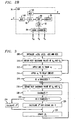
- linearizer 10 As illustrated in Fig. 1a.
- a radio frequency signal represented by frequency components 22 is fed to a power amplifier 12.
- Amplifier 12 generates additional intermodulation IM frequency components 24 because of its nonlinear response characteristics.
- Signal components 22' correspond to an amplified version of signal components 22.
- the function of linearizer 10 is to substantially eliminate frequency components 24, as explained in more detail below.
- Linearizer 10 includes a signal cancellation circuit 26 coupled to an error cancellation circuit 28.
- Signal cancellation circuit 26 has an upper branch that includes power amplifier 12, and a lower branch that provides the input signal of the linearizer to an input port of an adder 16 via a delay element 15.
- the other input port of adder 16 is configured to receive the output signal generated by power amplifier 12, via an attenuator 14.
- the output port of adder 16 provides signal components 24', which correspond to the attenuated version of intermodulation IM frequency components 24.
- delay element 15 is to assure that the input signal provided to adder 16 through the lower branch is aligned with the input signal provided through the upper branch.
- Error cancellation circuit 28 also includes an upper branch that is configured to provide the output signal generated by amplifier 12 to an adder 20 via a delay element 17.
- the lower branch of error cancellation circuit 28 includes an amplifier 18, which is configured to receive the attenuated intermodulation components 24'.
- Amplifier 18 generates an amplified version of signal 24' which is substantially equal to intermodulation component 24.
- the output port of adder 20 provides signal components 22' without the distortion caused by amplifier.
- the purpose of delay element 17 is to assure that the signal provided through the lower branch is aligned with the direct signal provided in the upper branch.
- the feedforward linearizer described in Fig. 1a has some disadvantages. For example, it is not able to adapt to signal changes. Furthermore, for wide-band input signals in the microwave frequency range, adjusting the delay in delay elements 15 and 17 is difficult. A small delay misalignment may lead to serious signal distortion. In order to provide a delay alignment between the upper and lower branches of the two cancellation circuits, some linearizers have been suggested that attempt to align the signal by trial and error during the operation. These linearizers employ a delay adjuster to achieve the intended delay alignment. However, the trial and error approach provides only limited accuracy and may lead to unacceptable output signal response.
- the bandwidth accommodated by power amplifier 12 is relatively small. Amplifiers that accommodate a large bandwidth are expensive. Thus, equalization for the power amplifier is required to increase the operating bandwidth so that the frequency response of the power amplifier is substantially flat.
- the prior art feedforward linearizers direct all the linear distortion caused by delay misalignment and the non-linear distortions caused by of the power amplifier to the auxiliary amplifier in the error cancellation loop.
- the auxiliary amplifier is designed as a class A amplifier. The distortion generated by the auxiliary amplifier itself is not recoverable. Thus, a high-accuracy class A amplifier that handles high power input is required in the error cancellation loop, which is expensive and difficult to design.
- European patent application EP-A-0675594 discloses a feedforward amplifier with reduced distortion in wide band. Specifically, a first pilot signal is superimposed onto an input signal thereto to distribute the signal as a first signal and a second signal to two destinations. The first signal is fed via an equalizer to a main amplifier for amplification thereof such that a second pilot signal is mixed with the amplified signal to attain a main amplification signal. Subtraction is conducted between the second signal and the main amplification signal to extract a distortion signal to be fed to an equalizer to an auxiliary amplifier so as to produce an auxiliary amplification signal. Between the main and auxiliary amplification signal, there is effected subtraction to attain a differential signal. The pilot signals are detected according to the differential output signals. The equalizers are controlled to set the pilot signals to a minimum value. Consequently, there is achieved a linear amplifier obtaining a stable amplification signal with reduced distortion in a wide band.
- a feedforward linearizer includes a signal cancellation circuit and an error cancellation circuit.
- the signal cancellation circuit includes a tap delay line, that delay the input signal by a predetermined time delay so as to provide several delayed versions of the input signal. Each delayed version of the input signal is weighted by a tap coefficient. The weighted signals are then added together and fed to the power amplifier.
- the tap coefficients are derived such that the signals traveling through the upper and lower branch of the signal cancellation loop are aligned and that the output signal of the power amplifier is equalized.
- the error cancellation circuit also includes a tap delay line, that delays the error signal to the error cancellation circuit by a predetermined time delay so as to provide several delayed versions of the error cancellation input signal. Each delayed version of the error cancellation input signal is weighted by a tap coefficient. The weighted signals are then added together and fed to an auxiliary amplifier. The tap coefficients in the error cancellation circuit are derived such that the signals traveling through the upper and lower branch of the error cancellation circuit are aligned.
- the tap coefficients are derived such that substantially no equalization for the auxiliary amplifier is achieved.
- Fig. 2 illustrates a wideband power amplifier feed-forward linearizer 60 in accordance with one embodiment of the invention, although the invention is not limited in scope in that respect.
- Linearizer 60 includes a signal cancellation circuit or loop 86 and an error cancellation loop or circuit 88. Each of the cancellation circuits 86 and 88 have two branches.
- signal cancellation circuit 86 includes a first signal cancellation branch that contains an amplifier 62, which is configured to receive an input signal V m , via a tap delay circuit 120. Input signal V m is also diverted to a second signal cancellation branch via signal splitter 122 and a delay element 124.
- the output port of power amplifier 62 provides an output signal V o and is coupled to an attenuator 64 having an attenuation factor r , via a splitter 90.
- the output port of attenuator 64 is coupled to an adder 68.
- the other input port of adder 68 is configured to receive the input signal V m , via delay element 124 in the second signal cancellation branch.
- the output port of adder 68 provides an error signal V d to error cancellation circuit 88.
- tap delay circuit 120 is employed to provide delay alignment and equalization in accordance with one embodiment of the invention.
- Delay circuit 120 includes a plurality of tap delay elements 112 that are configured to provide a predetermined delay ⁇ to signal V m .
- an input port of tap delay element 112a is configured to receive input signal V m .
- An output port of tap delay element 112a is coupled to an input port of the following tap delay element 112b, and so forth.
- the number of tap delay elements depends, among other things, on the delay mismatch ⁇ ⁇ , which is the delay difference between the upper and lower branches of the signal cancellation circuit.
- Delay circuit 120 also includes a plurality of multipliers, such as 92, 94 and 96, which are configured to receive signal V m , a first delayed version of input signal V m after it has been delayed by delay element 112a, and a second delayed version of input signal V m after it has been delayed by delay element 112b, and so forth.
- Each multiplier is configured to receive tap coefficients ⁇ i , wherein i is the index relating to the number of the tap delay element that provides a delayed version of V m to the multiplier.
- An output port of multipliers 92, 94 and 96 is coupled to an adder 130. The output port of adder 130 is in turn coupled to an input port of power amplifier 62.
- the output port of power amplifier 62 is also coupled to a first error cancellation branch of linearizer 60 via signal splitter 90.
- the first error cancellation branch includes a delay element 132 and an error cancellation adder 74 adapted to receive a delayed version of signal V o at one of its input ports.
- the second error cancellation branch of linearizer 60 includes a tap delay circuit 134 that is configured to receive the error signal V d at its input port.
- the output port of tap delay circuit 134 is coupled to an input port of an auxiliary amplifier 72.
- the output port of auxiliary amplifier 72 is coupled to the other input port of adder 74.
- the output port of adder 74 provides the output signal of linearizer 60.
- Delay circuit 134 also includes a plurality of multipliers, such as 98, 102 and 104, which are configured to receive the error signal V d , a first delayed version of input signal V d after it has been delayed by delay element 108a, and a second delayed version of input signal V d after it has been delayed by delay element 108b.
- Each multiplier is configured to receive a tap coefficient ⁇ i , wherein i is the index relating to the number of the tap delay element that provides a delayed version of V d to the multiplier.
- An output port of multipliers 98, 102 and 104 is coupled to an adder 70.
- the output port of adder 70 is in turn coupled to the input port of auxiliary amplifier 72.
- a digital signal processor 76 is configured to receive input signal, V m , error signal, V d , and the output signal V o .
- the digital signal processor as illustrated in Fig. 2b in accordance with one embodiment of the invention, includes a down converter circuit 84, which is configured to shift the frequency range of signals, V m , V d , and V o into the baseband frequency range, although the invention is not limited in scope in that respect.
- a separate down converter circuit in accordance with another embodiment of the invention, first shifts the frequencies to the baseband range, and then provides the down converted signal to digital signal processor 76.
- the output port of down converter circuit 84 is coupled to a digital signal processing circuit 80, via an analog-to-digital converter 92.
- Signal processing circuit 80 is configured to perform the necessary calculations to generate tap coefficients ⁇ i and ⁇ i and provide them respectively via multiplexers 140 and 142 to tap delay circuits 120 and 134.
- the arrangement of tap delay circuit 120 provides for a delay alignment and equalization at the same time in the signal cancellation circuit. Furthermore, the arrangement of tap delay circuit 134 provides for a delay alignment in the error cancellation circuit.
- the tap delay is chosen to be inversely proportional to the input signal bandwidth to achieve equalization. It is noted that for wideband input signals V m , T is substantially larger than ⁇ .
- LMS least mean square
- the solution to equation (2) in accordance with a least mean square algorithm provides both delay alignment and equalization at the same time.
- the converged solution ⁇ i to equation (2) may be deconvolved to two components, the first referred to as ⁇ d,i , and the second referred to as components ⁇ e,i , wherein ⁇ d,i are the desired tap coefficients when power amplifier 62 requires no equalization, and components ⁇ e,i are the desired tap coefficients when there is no delay misalignment between the two branches of signal cancellation circuit 86. It is also assumed that the delay difference between the two branches is ⁇ ⁇ when delay alignment is required.
- the intent is to adjust the tap coefficients ⁇ d,i , to introduce a delay ⁇ ⁇ , in a branch, other than the one that is generating an extra delay ⁇ ⁇ , which compensates for the existing delay between the two branches. Therefore, it is desired that the impulse response of the delay tap element to be ⁇ (t + ⁇ ⁇ ), where ⁇ (.) is an impulse function.
- the frequency response of ⁇ (t + ⁇ ⁇ ) is e - j2 ⁇ f ⁇ ⁇ , where f denotes the frequency. Since all the signals under consideration are band-limited signals, the frequency response may be truncated by a window without affecting the performance of the tap delay line.
- ⁇ 1 ⁇ 2 and ⁇ (x) 0 otherwise.
- the optimal tap coefficients ⁇ e,i for equalization with no delay misalignment is determined by the characteristics and operating range of power amplifier 62.
- the overall tap coefficients for delay circuit 120 is obtained as the convolution of ⁇ d,i and ⁇ e,i .
- the number of tap delay elements 112 depends on the ratio of ⁇ ⁇ / ⁇ . Thus if this ratio is close to an integer, ⁇ d,i will quickly converge to zero as
- the solution for error cancellation circuit 88 is described hereinafter.
- digital signal processor derives tap coefficients ⁇ i such that the error signal V d (kT) remains uncorrelated to the input signal V m (kT) .
- digital signal processor 76 controls the tap coefficients ⁇ i in the error cancellation circuit 88 such that the output signal V o (kT) is substantially uncorrelated with the error signal V d (kT) .
- a conventional least mean square algorithm for the error cancellation circuit 88 will cause output signal V o ( kT ) to be uncorrelated with not only V d (kT), but also to each error sample V d (kT) , V d (kT + ⁇ ), owing, V d ( kT + M ⁇ ).
- this solution may not be acceptable for some design specifications, because not only the error signal is substantially canceled, but some of the undistorted signal will be canceled also.
- this solution does not degrade the performance of linearizer 60.
- digital signal processor 76 employs a constrained version of a least mean square algorithm in accordance with one embodiment of the invention, although the invention is not limited in scope in this aspect.
- equation (5) provides for delay alignment between the two branches of the error cancellation circuit without canceling undistorted signals. It is noted that a least mean square algorithm that employs a constraint as specified in equation (5) will not provide for equalization. However, unlike power amplifier 62, auxiliary amplifier 72 is designed to perform acceptably without the need for equalization because of the relatively low power of V d .
- equation (5) suggests that there are three degrees of freedom relating to variable c r , c i , t , that may be employed to update coefficients ⁇ i , where c r , c i are respectively the real and imaginary parts of complex variable c in equation (5).
- the least mean square coefficient updates in equation (6) are projected on the subset defined in equation (5) before updating tap coefficients ⁇ i .
- the matrix applying pseudo-inverse in equation (9) [ ⁇ ( ⁇ )/ ⁇ ] is a (2M + 2) ⁇ 3 matrix and can be expanded as ⁇ Re ⁇ o k ⁇ c r ⁇ Re ⁇ o k ⁇ c i ⁇ Re ⁇ o k ⁇ t ⁇ ⁇ ⁇ ⁇ Re
- Fig. 3 illustrates a flow chart illustrating the steps accomplished by digital signal processing circuit 80 in accordance with one embodiment of the invention, although the invention is not limited in scope in that respect.
- processing circuit 80 initializes the values of ⁇ i ( 0 ), ⁇ i ( 0 ), c ( 0 ) and t ( 0 ).
- processing circuit 80 obtains the next available baseband input signals V m , and error signal V d .
- processing circuit 80 employs a least mean square algorithm to track the tap coefficients ⁇ i as explained in accordance with equation (2).
- the update values of tap coefficients ⁇ i are applied to delay circuit 120.
- the least mean square algorithm continues its estimation through an infinite loop of steps 210, 212 and 214 to track the variation of the input signal statistics and other environmental factors.
- processing circuit 80 determines at step 216 whether the value of tap coefficients ⁇ has been stabilized.
- processing circuit 80 proceeds to obtain tap coefficients ⁇ i for delay circuit 134 by obtaining the next available baseband value of V d and V o respectively.
- processing circuit 80 calculates the updated values p ( k ) in accordance with equation (6).
- processing circuit determines whether the delay adjustment variable, representing the delay difference between the upper and lower branches of error cancellation circuit 88, has been stabilized. If not, digital signal processing circuit 80 goes to step 224 and calculates ⁇ w in equation (9). Thereafter, processing circuit 80 goes to step 228 to update ⁇ in equation (8) and apply the updated tap coefficients to delay circuit 134.
- processing circuit 80 provides both equalization and delay adjustment in the signal cancellation circuit and provides delay adjustment in the error cancellation circuit.
- linearizer 60 provides a remarkable response.
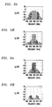
- Figs. 4(a) through 4(d) illustrate simulation results of linearizer 60 in accordance with one embodiment of the invention as described above.
- the input signal consists of eight tones with unit amplitude which are placed 300 kHz apart one after another.
- the central frequency is 900Mhz. Temperature and other environmental factors are assumed to be constant.
- ⁇ is set to be the reciprocal of the signal bandwidth.
- each delay circuit 120 and 134 employs seven tap delay elements.
- Figs. 4(a) -4(d) illustrated the performance of the system in accordance with one embodiment of the invention.
- Figs. 5(a)-5(b) illustrate the performance of an equivalent algorithm with the tap delay circuit replaced by a single-tap vector modulator, and the assumption that there are no delay mismatches between the upper and lower branches of both the cancellation circuits.
- Figs. 6(a) and 6(d) illustrate the performance of an equivalent algorithm with the tap delay circuit replaced by a single-tap vector modulator and the assumption that there is no distortion but there are delay mismatches between the upper and lower branches of both the cancellation circuits.
Landscapes
- Physics & Mathematics (AREA)
- Nonlinear Science (AREA)
- Engineering & Computer Science (AREA)
- Power Engineering (AREA)
- Amplifiers (AREA)
- Filters That Use Time-Delay Elements (AREA)
- Cable Transmission Systems, Equalization Of Radio And Reduction Of Echo (AREA)
Claims (20)
- Vorwärtskopplungs-Linearisierer (60) zum Verstärken eines Eingangssignals mit einer Signallöschschaltung (86) mit einem ersten Signallöschzweig und einem zweiten Signallöschzweig, gekennzeichnet durch:eine Signallöschverzögerungsschaltung (120) in dem ersten Signallöschzweig, die dafür konfiguriert ist, das Eingangssignal zu empfangen, wobei die Verzögerungsschaltung mehrere in Reihe geschaltete Abgriffverzögerungselemente aufweist, wobei jedes der Abgriffsverzögerungselemente eine verzögerte Version des Eingangssignals bereitstellt, wobei die Verzögerungsschaltung ferner mehrere Abgriffskoeffizientenmultiplizierer umfaßt, die jeweils an ein entsprechendes Abgriffsverzögerungselement angekoppelt sind, um so eine entsprechende der verzögerten Versionen des Eingangssignals zu empfangen und jede der verzögerten Versionen des Eingangssignals mit einem entsprechenden Abgriffskoeffizienten zu multiplizieren, wobei die Verzögerungsschaltung ferner einen an einen Ausgangsport jedes der Multiplizierer angekoppelten Verzögerungsschaltungsaddierer umfaßt, um so durch die Multiplizierer bereitgestellte Ausgangssignale zu addieren;einen in dem ersten Signallöschzweig bereitgestellten ersten Verstärker (62), wobei der Verstärker dafür konfiguriert ist, ein für Verstärkung bestimmtes Ausgangssignal des Verzögerungsschaltungsaddierers zu empfangen;einen Signallöschaddierer (68) der über ein Dämpfungsglied (64) an einen Ausgangsport des ersten Verstärkers (62) angekoppelt ist und über den zweiten Signallöschzweig an das Eingangssignal angekoppelt ist, um so ein Fehlersignal zu liefern;eine Fehlerlöschschaltung (88) mit einem ersten Fehlerlöschzweig und einem zweiten Fehlerlöschzweig;eine Fehlerlöschverzögerungsschaltung (134) mit mehreren in Reihe geschalteten Abgriffsverzögerungselementen, wobei jedes der Abgriffsverzögerungselemente eine verzögerte Version des Fehlersignals bereitstellt, wobei die Verzögerungsschaltung ferner mehrere Abgriffskoeffizientenmultiplizierer umfaßt, die jeweils an ein entsprechendes Abgriffsverzögerungselement angekoppelt sind, um so jede der verzögerten Versionen des Fehlersignals mit einem Abgriffskoeffizienten zu multiplizieren, wobei die Verzögerungsschaltung ferner einen an einen Ausgangsport jedes der Multiplizierer angekoppelten Verzögerungsschaltungsaddierer (70) umfaßt;einen in dem ersten Fehlerlöschzweig vorgesehenen zweiten Verstärker (72), wobei der Verstärker dafür konfiguriert ist, ein durch den Verzögerungsschaltungsaddierer bereitgestelltes Ausgangssignal zu empfangen;einen Fehlerlöschaddierer (74) in dem ersten Fehlerlöschzweig, wobei der Fehlerlöschaddierer (74) dafür konfiguriert ist, das durch den zweiten Verstärker (72) bereitgestellte Ausgangssignal zu empfangen;und außerdem zum Empfangen des Ausgangssignals des Signallöschaddierers (68);Bereitstellen des letztendlichen Linearisierungsausgangssignals; undeinen digitalen Signalprozessor (76), der dafür konfiguriert ist, die Signallöschverzögerungseinstellkoeffizienten αi den Abgriffskoeffizientenmultiplizierern und Fehlersignallöschverzögerungseinstellkoeffizienten βi den Abgriffskoeffizientenmultiplizierern zuzuführen, dergestalt, daß die Verzögerung in dem oberen und dem unteren Zweig beider Löschschaltungen im wesentlichen ausgerichtet ist und das Ausgangssignal des ersten Verstärkers im wesentlichen entzerrt wird.
- Vorwärtskopplungs-Linearisierer nach Anspruch 1, wobei der digitale Signalprozessor einen Least-Mean-Square-Kalkulator umfaßt, der die Verzögerungseinstellkoeffizienten für die Signallöschverzögerungsschaltung durch Verwendung eines Least-Mean-Square-Algorithmus berechnet.
- Vorwärtskopplungs-Linearisierer nach Anspruch 2, wobei die Verzögerungselemente in der Signallöschverzögerungsschaltung eine Verzögerung bereitstellen, die im wesentlichen gleich dem Kehrwert der Bandbreite des Eingangssignals ist.
- Vorwärtskopplungs-Linearisierer nach Anspruch 3, ferner mit einem Dämpfungsglied, das an den ersten Verstärker angekoppelt ist und dafür konfiguriert ist, die durch den ersten Verstärker bereitgestellten verstärkten Signale zu empfangen und die Signale zu dämpfen, um so dem Signallöschaddierer eine gedämpfte Version der verstärkten Signale zuzuführen.
- Vorwärtskopplungs-Linearisierer nach Anspruch 1, wobei der digitale Signalprozessor einen Least-Mean-Square-Kalkulator umfaßt, der die Einstellungskoeffizientensignale βi für die Fehlerlöschverzögerungsschaltung durch Verwendung eines eingeschränkten Least-Mean-Square-Algorithmus berechnet.
- Vorwärtskopplungs-Linearisierer nach Anspruch 5, wobei der Least-Mean-Square-Kalkulator einen eingeschränkten Least-Mean-Square-Algorithmus verwendet, indem Least-Mean-Square-Koeffizientenaktualisierungen


- Integrierte Schaltung mit einem Vorwärtskopplungs-Linearisierer nach Anspruch 1.
- Vorwärtskopplungs-Linearisierer (60) zum Verstärken eines Eingangssignals durch einen Leistungsverstärker, wobei der Linearisierer eine Signallöschschaltung aufweist, mit einer Signallöschverzögerungsschaltung (120) in der Signallöschschaltung (86), gekennzeichnet durch:mehrere Abgriffsverzögerungselemente (112a, 112b), die an das Eingangssignal angekoppelt und in Reihe geschaltet sind, dergestalt, daß jedes der Abgriffsverzögerungselemente eine verzögerte Version des Eingangssignals bereitstellt;mehrere Abgriffskoeffizientenmultiplizierer (92, 94, 96), die jeweils an ein entsprechendes Abgriffsverzögerungselement angekoppelt sind, um so eine entsprechende der verzögerten Versionen des Eingangssignals zu empfangen und jede der verzögerten Versionen des Eingangssignals mit einem entsprechenden Abgriffskoeffizienten zu multiplizieren;einen Verzögerungsschaltungsaddierer (130), der an einen Ausgangsport jedes der Multiplizierer angekoppelt ist, um so durch jeden der Multiplizierer bereitgestellte Ausgangssignale zu addieren und dem Leistungsverstärker ein summiertes Signal zuzuführen.
- Vorwärtskopplungs-Linearisierer (60) zum Verstärken eines Eingangssignals durch einen Leistungsverstärker, wobei der Linearisierer eine Signallöschschaltung, die ein Fehlersignal erzeugt, und eine Fehlerlöschschaltung mit einem auf das Fehlersignal ansprechenden Hilfsverstärker aufweist, mit einer Fehlerlöschverzögerungsschaltung (134) in der Fehlerlöschschaltung (88), gekennzeichnet durch:mehrere Abgriffsverzögerungselemente (108a, 108b), die an das Fehlersignal angekoppelt und in Reihe geschaltet sind, dergestalt, daß jedes der Abgriffsverzögerungselemente eine verzögerte Version des Fehlersignals bereitstellt;mehrere Abgriffskoeffizientenmultiplizierer (98, 102, 104), die jeweils an ein entsprechendes Abgriffsverzögerungselement angekoppelt sind, um so jede der verzögerten Versionen des Fehlersignals mit einem Abgriffskoeffizienten zu multiplizieren;einen Verzögerungsschaltungsaddierer (70), der an einen Ausgangsport jedes der Multiplizierer angekoppelt ist, um dem Hilfsverstärker ein summiertes Signal zuzuführen.
- Fehlerlöschverzögerungsschaltung nach Anspruch 9, wobei die Abgriffskoeffizienten βi gemäß einem eingeschränkten Least-Square-Algorithmus berechnet werden, dergestalt, daß die Least-Mean-Square-Koeffizientenaktualisierungen


- Schaltung nach Anspruch 8 oder 9, wobei die Verzögerung der Abgriffsverzögerungselemente umgekehrt proportional zu der Bandbreite des Eingangssignals ist.
- Schaltung nach Anspruch 11, wobei die Signallöschschleife einen oberen Zweig zum Führen des Eingangssignals durch die Verzögerungsschaltung und den Leistungsverstärker zu einem Signallöschaddierer und einen unteren Zweig zum Führen des Eingangssignals zu dem Signallöschaddierer umfaßt, wobei das Eingangssignal innerhalb einer Verzögerungsperiode, die als Verzögerungsfehlausrichtung definiert wird, an dem Signallöschaddierer ankommt.
- Schaltung nach Anspruch 8 oder 9, wobei die Abgriffskoeffizienten durch einen digitalen Signalprozessor erzeugt werden.
- Schaltung nach Anspruch 13, wobei der digitale Signalprozessor die Abgriffskoeffizienten gemäß einem Least-Square-Algorithmus berechnet.
- Verfahren zur Verwendung in einem Vorwärtskopplungs-Linearisierer (60) zum Verstärken eines Eingangssignals durch einen Leistungsverstärker, wobei der Linearisierer eine Signallöschschaltung, die ein Fehlersignal erzeugt, und eine Fehlerlöschschaltung mit einem auf das Fehlersignal ansprechenden Hilfsverstärker aufweist, wobei das Verfahren zum Linearisieren des Verstärkers durch die folgenden Schritte gekennzeichnet ist:Bereitstellen (120) mehrerer verzögerter Versionen des Eingangssignals;Multiplizieren (92, 94, 96) jeder der verzögerten Versionen des Eingangssignals mit einem entsprechenden Signallösch-Abgriffskoeffizienten;Addieren (130), der aus dem Multiplikationsschritt erzeugten Signale, um so dem Leistungsverstärker ein summiertes Signal zuzuführen;Bereitstellen (134) mehrerer verzögerter Versionen des Fehlersignals;Multiplizieren (98, 102, 104) jeder der verzögerten Versionen des Fehlersignals mit einem Abgriffskoeffizienten; undAddieren (70) der multiplizierten Fehlersignale, um so dem Hilfsverstärker ein summiertes Signal zuzuführen.
- Verfahren nach Anspruch 15, ferner mit den folgenden Schritten:Führen des Fehlersignals zu einem Fehlerlöschaddierer durch einen unteren Zweig der Fehlerlöschschaltung und Führen eines Ausgangssignals des Leistungsverstärkers zu dem Fehlerlöschaddierer durch einen oberen Zweig der Fehlerlöschschaltung, wobei die Signale innerhalb einer Verzögerungsperiode, die als Verzögerungsfehlausrichtung definiert wird, an dem Fehlerlöschaddierer ankommen.
- Verfahren nach Anspruch 15, wobei die Verzögerung der Abgriffsverzögerungselemente umgekehrt proportional zu der Bandbreite des Eingangssignals ist.
- Verfahren nach Anspruch 15, ferner mit dem Schritt des Erzeugens der Abgriffskoeffizienten durch einen digitalen Signalprozessor.
- Verfahren nach Anspruch 18, wobei der digitale Signalprozessor die Abgriffskoeffizienten gemäß einem Least-Square-Algorithmus berechnet.
- Verfahren nach Anspruch 19, ferner mit dem Schritt des Berechnens der Abgriffskoeffizienten βi gemäß einem eingeschränkten Least-Square-Algorithmus dergestalt, daß Least-Mean-Square-Koeffizientenaktualisierungen


Applications Claiming Priority (2)
| Application Number | Priority Date | Filing Date | Title |
|---|---|---|---|
| US09/041,604 US6172565B1 (en) | 1998-03-13 | 1998-03-13 | Adaptive joint linearization, equalization and delay alignment for a wideband power amplifier |
| US41604 | 1998-03-13 |
Publications (2)
| Publication Number | Publication Date |
|---|---|
| EP0942525A1 EP0942525A1 (de) | 1999-09-15 |
| EP0942525B1 true EP0942525B1 (de) | 2007-07-11 |
Family
ID=21917417
Family Applications (1)
| Application Number | Title | Priority Date | Filing Date |
|---|---|---|---|
| EP99301791A Expired - Lifetime EP0942525B1 (de) | 1998-03-13 | 1999-03-09 | Selbsttätiges gemeinsames Ausrichten von Lineariserung, Entzerrung und der Verzögerung in einem Breitbandleistungsverstärker |
Country Status (4)
| Country | Link |
|---|---|
| US (1) | US6172565B1 (de) |
| EP (1) | EP0942525B1 (de) |
| JP (1) | JP3443536B2 (de) |
| DE (1) | DE69936481T2 (de) |
Families Citing this family (12)
| Publication number | Priority date | Publication date | Assignee | Title |
|---|---|---|---|---|
| CA2281209A1 (en) * | 1998-10-30 | 2000-04-30 | Norman Gerard Ziesse | Feedforward amplifier and method of amplifying signals |
| US6208207B1 (en) * | 1999-05-05 | 2001-03-27 | Simon Fraser University | Adaptive linearizer for RF power amplifiers |
| US6320461B1 (en) * | 2000-05-12 | 2001-11-20 | Jhong Sam Lee | Ultra-linear feedforward RF power amplifier |
| US7231191B2 (en) * | 2001-09-28 | 2007-06-12 | Powerwave Technologies, Inc. | Spurious ratio control circuit for use with feed-forward linear amplifiers |
| US6794938B2 (en) * | 2002-03-19 | 2004-09-21 | The University Of North Carolina At Charlotte | Method and apparatus for cancellation of third order intermodulation distortion and other nonlinearities |
| US6765440B2 (en) * | 2002-12-18 | 2004-07-20 | Andrew Corporation | Model-based feed-forward linearization of amplifiers |
| US6985706B2 (en) * | 2003-01-23 | 2006-01-10 | Powerwave Technologies, Inc. | Feed forward amplifier system employing self-generating alignment lists and adaptive controller |
| DE602005023551D1 (de) * | 2004-01-28 | 2010-10-28 | Ntt Docomo Inc | Mehrfachband-Vorwärtskopplungsverstärker und Methode zur Einstellung desselben |
| US7157967B2 (en) * | 2004-03-11 | 2007-01-02 | Powerwave Technologies Inc. | System and method for control of loop alignment in adaptive feed forward amplifiers |
| US10193683B2 (en) * | 2016-07-20 | 2019-01-29 | Intel Corporation | Methods and devices for self-interference cancelation |
| US9859844B1 (en) | 2016-10-10 | 2018-01-02 | Sebastien Amiot | Power amplifier circuit and method of design |
| EP4418535A4 (de) * | 2021-11-18 | 2024-11-27 | Huawei Technologies Co., Ltd. | Signalverarbeitungsvorrichtung und kommunikationsvorrichtung |
Family Cites Families (6)
| Publication number | Priority date | Publication date | Assignee | Title |
|---|---|---|---|---|
| US5049832A (en) | 1990-04-20 | 1991-09-17 | Simon Fraser University | Amplifier linearization by adaptive predistortion |
| GB9009295D0 (en) * | 1990-04-25 | 1990-06-20 | Kenington Peter B | Apparatus and method for reducing distortion in amplification |
| JP2746107B2 (ja) | 1994-03-31 | 1998-04-28 | 日本電気株式会社 | フィードフォワード増幅器 |
| JP3320210B2 (ja) * | 1994-05-31 | 2002-09-03 | 富士通株式会社 | 初期動作時不要波出力防止型フィードフォワード増幅装置 |
| US5489875A (en) | 1994-09-21 | 1996-02-06 | Simon Fraser University | Adaptive feedforward linearizer for RF power amplifiers |
| EP0729228B1 (de) | 1995-02-22 | 2003-01-15 | STMicroelectronics S.r.l. | Basiszelle für ein analoges programmierbares zeitkontinuierliches Filter |
-
1998
- 1998-03-13 US US09/041,604 patent/US6172565B1/en not_active Expired - Lifetime
-
1999
- 1999-03-09 EP EP99301791A patent/EP0942525B1/de not_active Expired - Lifetime
- 1999-03-09 DE DE69936481T patent/DE69936481T2/de not_active Expired - Lifetime
- 1999-03-10 JP JP06412599A patent/JP3443536B2/ja not_active Expired - Fee Related
Also Published As
| Publication number | Publication date |
|---|---|
| DE69936481D1 (de) | 2007-08-23 |
| EP0942525A1 (de) | 1999-09-15 |
| JPH11330868A (ja) | 1999-11-30 |
| DE69936481T2 (de) | 2008-03-13 |
| US6172565B1 (en) | 2001-01-09 |
| JP3443536B2 (ja) | 2003-09-02 |
Similar Documents
| Publication | Publication Date | Title |
|---|---|---|
| US20230370937A1 (en) | Method and system for baseband predistortion linearization in multi-channel wideband communication systems | |
| US7418056B2 (en) | Digital predistorter using power series model | |
| US7071777B2 (en) | Digital memory-based predistortion technique | |
| US7415252B2 (en) | Arrangement and method for digital predistortion of a complex baseband input signal | |
| KR100338230B1 (ko) | 알에프 전력증폭기의 적응형 디지털 사전왜곡 선형화 및 피드-포워드 정정 | |
| CN100559720C (zh) | 用于使得具有非线性增益特性和记忆效应的rf功率放大器线性化的数字预失真系统和方法 | |
| US7149257B2 (en) | Digital predistortion system and method for correcting memory effects within an RF power amplifier | |
| US7269231B2 (en) | System and method for predistorting a signal using current and past signal samples | |
| JP3393650B2 (ja) | 適応型アンプ歪補償回路 | |
| US6794939B2 (en) | Signal predistortion using a combination of multiple predistortion techniques | |
| US6377116B1 (en) | Pre-distorter and corresponding method for deriving same | |
| US20060133536A1 (en) | Power amplifier pre-distortion | |
| US20020171485A1 (en) | Digitally implemented predistorter control mechanism for linearizing high efficiency RF power amplifiers | |
| US20060012427A1 (en) | Estimating power amplifier non-linearity in accordance with memory depth | |
| EP0942525B1 (de) | Selbsttätiges gemeinsames Ausrichten von Lineariserung, Entzerrung und der Verzögerung in einem Breitbandleistungsverstärker | |
| KR20000067950A (ko) | 적응성 사전왜곡회로를 갖는 알에프 증폭기 | |
| US7015751B2 (en) | Decorrelated power amplifier linearizers | |
| US7239203B2 (en) | LMS-based adaptive pre-distortion for enhanced power amplifier efficiency | |
| US7924942B2 (en) | Power amplifier pre-distortion | |
| US7391822B2 (en) | Method and apparatus for estimating a sample delay between a transmission signal and a feedback signal in a mobile communication system, and a base station transmitter using the same | |
| Bremond et al. | PROBLEM 3: MATHEMATICAL MODELING OF HIGH POWER AMPLIFIER (HPA) AND HPA LINEARIZATION THROUGH A PREDISTORTER |
Legal Events
| Date | Code | Title | Description |
|---|---|---|---|
| PUAI | Public reference made under article 153(3) epc to a published international application that has entered the european phase |
Free format text: ORIGINAL CODE: 0009012 |
|
| AK | Designated contracting states |
Kind code of ref document: A1 Designated state(s): DE FR GB |
|
| AX | Request for extension of the european patent |
Free format text: AL;LT;LV;MK;RO;SI |
|
| RIN1 | Information on inventor provided before grant (corrected) |
Inventor name: CHEN, YOUNG-KAI Inventor name: TSAI, HUAN-SHANG Inventor name: CHEN, JIUNN-TSAIR |
|
| 17P | Request for examination filed |
Effective date: 20000302 |
|
| AKX | Designation fees paid |
Free format text: DE FR GB |
|
| GRAP | Despatch of communication of intention to grant a patent |
Free format text: ORIGINAL CODE: EPIDOSNIGR1 |
|
| GRAS | Grant fee paid |
Free format text: ORIGINAL CODE: EPIDOSNIGR3 |
|
| GRAA | (expected) grant |
Free format text: ORIGINAL CODE: 0009210 |
|
| AK | Designated contracting states |
Kind code of ref document: B1 Designated state(s): DE FR GB |
|
| REG | Reference to a national code |
Ref country code: GB Ref legal event code: FG4D |
|
| REF | Corresponds to: |
Ref document number: 69936481 Country of ref document: DE Date of ref document: 20070823 Kind code of ref document: P |
|
| ET | Fr: translation filed | ||
| PLBE | No opposition filed within time limit |
Free format text: ORIGINAL CODE: 0009261 |
|
| STAA | Information on the status of an ep patent application or granted ep patent |
Free format text: STATUS: NO OPPOSITION FILED WITHIN TIME LIMIT |
|
| 26N | No opposition filed |
Effective date: 20080414 |
|
| REG | Reference to a national code |
Ref country code: GB Ref legal event code: 732E Free format text: REGISTERED BETWEEN 20131107 AND 20131113 |
|
| REG | Reference to a national code |
Ref country code: FR Ref legal event code: CD Owner name: ALCATEL-LUCENT USA INC. Effective date: 20131122 |
|
| REG | Reference to a national code |
Ref country code: FR Ref legal event code: GC Effective date: 20140410 |
|
| REG | Reference to a national code |
Ref country code: FR Ref legal event code: RG Effective date: 20141015 |
|
| REG | Reference to a national code |
Ref country code: FR Ref legal event code: PLFP Year of fee payment: 17 |
|
| REG | Reference to a national code |
Ref country code: FR Ref legal event code: PLFP Year of fee payment: 18 |
|
| PGFP | Annual fee paid to national office [announced via postgrant information from national office to epo] |
Ref country code: FR Payment date: 20160321 Year of fee payment: 18 Ref country code: GB Payment date: 20160321 Year of fee payment: 18 |
|
| PGFP | Annual fee paid to national office [announced via postgrant information from national office to epo] |
Ref country code: DE Payment date: 20160330 Year of fee payment: 18 |
|
| REG | Reference to a national code |
Ref country code: DE Ref legal event code: R119 Ref document number: 69936481 Country of ref document: DE |
|
| GBPC | Gb: european patent ceased through non-payment of renewal fee |
Effective date: 20170309 |
|
| REG | Reference to a national code |
Ref country code: FR Ref legal event code: ST Effective date: 20171130 |
|
| PG25 | Lapsed in a contracting state [announced via postgrant information from national office to epo] |
Ref country code: DE Free format text: LAPSE BECAUSE OF NON-PAYMENT OF DUE FEES Effective date: 20171003 Ref country code: FR Free format text: LAPSE BECAUSE OF NON-PAYMENT OF DUE FEES Effective date: 20170331 |
|
| PG25 | Lapsed in a contracting state [announced via postgrant information from national office to epo] |
Ref country code: GB Free format text: LAPSE BECAUSE OF NON-PAYMENT OF DUE FEES Effective date: 20170309 |