EP0939061A1 - Joining material for electronic components, electronic components and a method for manufacturing the same - Google Patents
Joining material for electronic components, electronic components and a method for manufacturing the same Download PDFInfo
- Publication number
- EP0939061A1 EP0939061A1 EP99301394A EP99301394A EP0939061A1 EP 0939061 A1 EP0939061 A1 EP 0939061A1 EP 99301394 A EP99301394 A EP 99301394A EP 99301394 A EP99301394 A EP 99301394A EP 0939061 A1 EP0939061 A1 EP 0939061A1
- Authority
- EP
- European Patent Office
- Prior art keywords
- mol
- layer
- joining
- joining material
- glass
- Prior art date
- Legal status (The legal status is an assumption and is not a legal conclusion. Google has not performed a legal analysis and makes no representation as to the accuracy of the status listed.)
- Granted
Links
Images


Classifications
-
- C—CHEMISTRY; METALLURGY
- C03—GLASS; MINERAL OR SLAG WOOL
- C03C—CHEMICAL COMPOSITION OF GLASSES, GLAZES OR VITREOUS ENAMELS; SURFACE TREATMENT OF GLASS; SURFACE TREATMENT OF FIBRES OR FILAMENTS MADE FROM GLASS, MINERALS OR SLAGS; JOINING GLASS TO GLASS OR OTHER MATERIALS
- C03C8/00—Enamels; Glazes; Fusion seal compositions being frit compositions having non-frit additions
- C03C8/24—Fusion seal compositions being frit compositions having non-frit additions, i.e. for use as seals between dissimilar materials, e.g. glass and metal; Glass solders
-
- C—CHEMISTRY; METALLURGY
- C03—GLASS; MINERAL OR SLAG WOOL
- C03C—CHEMICAL COMPOSITION OF GLASSES, GLAZES OR VITREOUS ENAMELS; SURFACE TREATMENT OF GLASS; SURFACE TREATMENT OF FIBRES OR FILAMENTS MADE FROM GLASS, MINERALS OR SLAGS; JOINING GLASS TO GLASS OR OTHER MATERIALS
- C03C8/00—Enamels; Glazes; Fusion seal compositions being frit compositions having non-frit additions
- C03C8/14—Glass frit mixtures having non-frit additions, e.g. opacifiers, colorants, mill-additions
-
- C—CHEMISTRY; METALLURGY
- C04—CEMENTS; CONCRETE; ARTIFICIAL STONE; CERAMICS; REFRACTORIES
- C04B—LIME, MAGNESIA; SLAG; CEMENTS; COMPOSITIONS THEREOF, e.g. MORTARS, CONCRETE OR LIKE BUILDING MATERIALS; ARTIFICIAL STONE; CERAMICS; REFRACTORIES; TREATMENT OF NATURAL STONE
- C04B37/00—Joining burned ceramic articles with other burned ceramic articles or other articles by heating
- C04B37/003—Joining burned ceramic articles with other burned ceramic articles or other articles by heating by means of an interlayer consisting of a combination of materials selected from glass, or ceramic material with metals, metal oxides or metal salts
- C04B37/005—Joining burned ceramic articles with other burned ceramic articles or other articles by heating by means of an interlayer consisting of a combination of materials selected from glass, or ceramic material with metals, metal oxides or metal salts consisting of glass or ceramic material
-
- H—ELECTRICITY
- H01—ELECTRIC ELEMENTS
- H01G—CAPACITORS; CAPACITORS, RECTIFIERS, DETECTORS, SWITCHING DEVICES OR LIGHT-SENSITIVE DEVICES, OF THE ELECTROLYTIC TYPE
- H01G4/00—Fixed capacitors; Processes of their manufacture
- H01G4/30—Stacked capacitors
-
- C—CHEMISTRY; METALLURGY
- C04—CEMENTS; CONCRETE; ARTIFICIAL STONE; CERAMICS; REFRACTORIES
- C04B—LIME, MAGNESIA; SLAG; CEMENTS; COMPOSITIONS THEREOF, e.g. MORTARS, CONCRETE OR LIKE BUILDING MATERIALS; ARTIFICIAL STONE; CERAMICS; REFRACTORIES; TREATMENT OF NATURAL STONE
- C04B2235/00—Aspects relating to ceramic starting mixtures or sintered ceramic products
- C04B2235/70—Aspects relating to sintered or melt-casted ceramic products
- C04B2235/96—Properties of ceramic products, e.g. mechanical properties such as strength, toughness, wear resistance
- C04B2235/9646—Optical properties
- C04B2235/9661—Colour
-
- C—CHEMISTRY; METALLURGY
- C04—CEMENTS; CONCRETE; ARTIFICIAL STONE; CERAMICS; REFRACTORIES
- C04B—LIME, MAGNESIA; SLAG; CEMENTS; COMPOSITIONS THEREOF, e.g. MORTARS, CONCRETE OR LIKE BUILDING MATERIALS; ARTIFICIAL STONE; CERAMICS; REFRACTORIES; TREATMENT OF NATURAL STONE
- C04B2237/00—Aspects relating to ceramic laminates or to joining of ceramic articles with other articles by heating
- C04B2237/02—Aspects relating to interlayers, e.g. used to join ceramic articles with other articles by heating
- C04B2237/10—Glass interlayers, e.g. frit or flux
-
- C—CHEMISTRY; METALLURGY
- C04—CEMENTS; CONCRETE; ARTIFICIAL STONE; CERAMICS; REFRACTORIES
- C04B—LIME, MAGNESIA; SLAG; CEMENTS; COMPOSITIONS THEREOF, e.g. MORTARS, CONCRETE OR LIKE BUILDING MATERIALS; ARTIFICIAL STONE; CERAMICS; REFRACTORIES; TREATMENT OF NATURAL STONE
- C04B2237/00—Aspects relating to ceramic laminates or to joining of ceramic articles with other articles by heating
- C04B2237/30—Composition of layers of ceramic laminates or of ceramic or metallic articles to be joined by heating, e.g. Si substrates
- C04B2237/32—Ceramic
- C04B2237/34—Oxidic
- C04B2237/345—Refractory metal oxides
- C04B2237/346—Titania or titanates
-
- C—CHEMISTRY; METALLURGY
- C04—CEMENTS; CONCRETE; ARTIFICIAL STONE; CERAMICS; REFRACTORIES
- C04B—LIME, MAGNESIA; SLAG; CEMENTS; COMPOSITIONS THEREOF, e.g. MORTARS, CONCRETE OR LIKE BUILDING MATERIALS; ARTIFICIAL STONE; CERAMICS; REFRACTORIES; TREATMENT OF NATURAL STONE
- C04B2237/00—Aspects relating to ceramic laminates or to joining of ceramic articles with other articles by heating
- C04B2237/50—Processing aspects relating to ceramic laminates or to the joining of ceramic articles with other articles by heating
- C04B2237/59—Aspects relating to the structure of the interlayer
- C04B2237/592—Aspects relating to the structure of the interlayer whereby the interlayer is not continuous, e.g. not the whole surface of the smallest substrate is covered by the interlayer
-
- C—CHEMISTRY; METALLURGY
- C04—CEMENTS; CONCRETE; ARTIFICIAL STONE; CERAMICS; REFRACTORIES
- C04B—LIME, MAGNESIA; SLAG; CEMENTS; COMPOSITIONS THEREOF, e.g. MORTARS, CONCRETE OR LIKE BUILDING MATERIALS; ARTIFICIAL STONE; CERAMICS; REFRACTORIES; TREATMENT OF NATURAL STONE
- C04B2237/00—Aspects relating to ceramic laminates or to joining of ceramic articles with other articles by heating
- C04B2237/50—Processing aspects relating to ceramic laminates or to the joining of ceramic articles with other articles by heating
- C04B2237/66—Forming laminates or joined articles showing high dimensional accuracy, e.g. indicated by the warpage
-
- C—CHEMISTRY; METALLURGY
- C04—CEMENTS; CONCRETE; ARTIFICIAL STONE; CERAMICS; REFRACTORIES
- C04B—LIME, MAGNESIA; SLAG; CEMENTS; COMPOSITIONS THEREOF, e.g. MORTARS, CONCRETE OR LIKE BUILDING MATERIALS; ARTIFICIAL STONE; CERAMICS; REFRACTORIES; TREATMENT OF NATURAL STONE
- C04B2237/00—Aspects relating to ceramic laminates or to joining of ceramic articles with other articles by heating
- C04B2237/50—Processing aspects relating to ceramic laminates or to the joining of ceramic articles with other articles by heating
- C04B2237/70—Forming laminates or joined articles comprising layers of a specific, unusual thickness
- C04B2237/704—Forming laminates or joined articles comprising layers of a specific, unusual thickness of one or more of the ceramic layers or articles
-
- C—CHEMISTRY; METALLURGY
- C04—CEMENTS; CONCRETE; ARTIFICIAL STONE; CERAMICS; REFRACTORIES
- C04B—LIME, MAGNESIA; SLAG; CEMENTS; COMPOSITIONS THEREOF, e.g. MORTARS, CONCRETE OR LIKE BUILDING MATERIALS; ARTIFICIAL STONE; CERAMICS; REFRACTORIES; TREATMENT OF NATURAL STONE
- C04B2237/00—Aspects relating to ceramic laminates or to joining of ceramic articles with other articles by heating
- C04B2237/50—Processing aspects relating to ceramic laminates or to the joining of ceramic articles with other articles by heating
- C04B2237/70—Forming laminates or joined articles comprising layers of a specific, unusual thickness
- C04B2237/708—Forming laminates or joined articles comprising layers of a specific, unusual thickness of one or more of the interlayers
-
- C—CHEMISTRY; METALLURGY
- C04—CEMENTS; CONCRETE; ARTIFICIAL STONE; CERAMICS; REFRACTORIES
- C04B—LIME, MAGNESIA; SLAG; CEMENTS; COMPOSITIONS THEREOF, e.g. MORTARS, CONCRETE OR LIKE BUILDING MATERIALS; ARTIFICIAL STONE; CERAMICS; REFRACTORIES; TREATMENT OF NATURAL STONE
- C04B2237/00—Aspects relating to ceramic laminates or to joining of ceramic articles with other articles by heating
- C04B2237/50—Processing aspects relating to ceramic laminates or to the joining of ceramic articles with other articles by heating
- C04B2237/72—Forming laminates or joined articles comprising at least two interlayers directly next to each other
-
- Y—GENERAL TAGGING OF NEW TECHNOLOGICAL DEVELOPMENTS; GENERAL TAGGING OF CROSS-SECTIONAL TECHNOLOGIES SPANNING OVER SEVERAL SECTIONS OF THE IPC; TECHNICAL SUBJECTS COVERED BY FORMER USPC CROSS-REFERENCE ART COLLECTIONS [XRACs] AND DIGESTS
- Y10—TECHNICAL SUBJECTS COVERED BY FORMER USPC
- Y10T—TECHNICAL SUBJECTS COVERED BY FORMER US CLASSIFICATION
- Y10T428/00—Stock material or miscellaneous articles
- Y10T428/11—Magnetic recording head
- Y10T428/1193—Magnetic recording head with interlaminar component [e.g., adhesion layer, etc.]
-
- Y—GENERAL TAGGING OF NEW TECHNOLOGICAL DEVELOPMENTS; GENERAL TAGGING OF CROSS-SECTIONAL TECHNOLOGIES SPANNING OVER SEVERAL SECTIONS OF THE IPC; TECHNICAL SUBJECTS COVERED BY FORMER USPC CROSS-REFERENCE ART COLLECTIONS [XRACs] AND DIGESTS
- Y10—TECHNICAL SUBJECTS COVERED BY FORMER USPC
- Y10T—TECHNICAL SUBJECTS COVERED BY FORMER US CLASSIFICATION
- Y10T428/00—Stock material or miscellaneous articles
- Y10T428/24—Structurally defined web or sheet [e.g., overall dimension, etc.]
- Y10T428/24802—Discontinuous or differential coating, impregnation or bond [e.g., artwork, printing, retouched photograph, etc.]
- Y10T428/24917—Discontinuous or differential coating, impregnation or bond [e.g., artwork, printing, retouched photograph, etc.] including metal layer
Definitions
- the invention relates to a joining material for an electronic component, such as capacitor, inductors, resistors, stacked type and coaxial type dielectric filters, Stacked type LC filters, composite LC components and composite LCR modules, an electronic component and a method for manufacturing the same.
- an electronic component such as capacitor, inductors, resistors, stacked type and coaxial type dielectric filters, Stacked type LC filters, composite LC components and composite LCR modules, an electronic component and a method for manufacturing the same.
- a paste for an internal layer electrode is printed on each of a predetermined number of greensheets, which are then laminated to produce laminated greensheets.
- This laminated greensheets are then sintered at a temperature of 700°C to 1100°C to produce a base body with the internal layer electrodes.
- a metal paste for an outer electrode is printed on predetermined regions on the surface of the body and fired to form the outer electrodes.
- a composite LC filter with an inductor and capacitor is also known.
- a predetermined number of greensheets for, for example, a dielectric layer and magnetic layer are laminated to provide laminated greensheets, which are then co-fired to join the magnetic and dielectric layers. It is also known to provide a greensheet of a joining layer between the greensheets of the magnetic and dielectric layers to provide laminated greensheets which are then co-fired.
- a ceramic material obtained by firing a mixture of ZnO, TiO 2 and CuO, is used for the joining layer for preventing the peeling between the dielectric layers and magnetic layers and diffusion of the ingredients of both layers with each other.
- a ceramic material is provided between the dielectric and magnetic layers for improving the adhesive strength of the layers and for preventing diffusion of the ingredients of both layers with each other, the ceramic material being obtained by mixing a glass contained in the dielectric layer with a ceramic of 15 to 40 mol% of BaO and 60 to 85 mol% of TiO 2 and firing.
- warp may occur in the magnetic or dielectric layer depending on the compositions of both layers and their firing schedule.
- the amount of warp is out of the specification for manufacturing a filter, such filter with impermissible warp is discarded as a defective, thus decreasing its manufacturing yield.
- the inventors further found that warp was also induced in the layers during sintering process.
- the object of the invention is, in an electronic component having a plurality of functional layers each selected from a magnetic layer and dielectric layer and joined with each other, to prevent warp in the magnetic layers or the dielectric layer.
- the invention may be stated as providing a joining material suitable for joining functional layers of an electronic component, which joining material is composed of a glass and a composition containing from 12 to 45 mol% of ZnO, from 4-45 mol% of BaO, from 18-81 mol% of TiO 2 and optionally upto 40 mol% of other metal oxides, preferably not more than 30, 20 or even not more than 10 mol% of other metal oxides.
- Preferences for these other metal oxides are not more than 10% of manganese oxide and/or not more than 10% of Al 2 O 3 , and not more than 10% of a metal oxide which is Y 2 0 3 , ZrO 2 or a mixture of them, and/or not more than 10% of a metal oxide selected from a group consisting of Cr 2 0 3 , Fe 2 0 3 and NiO and mixtures of them.
- the invention also provides a method of making a joining material by mixing a said composition of metal oxides and a glass in proportions of 0.1-10 weight parts of the glass per 100 weight parts of the composition.
- the invention also provides an electronic component having the functional layers and a joining layer for joining the adjacent functional layers, wherein the joining layer is composed of sintered product of each of the joining materials. That is, a layer composed of each of the joining materials is fired to form the joining layer.
- the joining layer is made of the sintered product obtained by firing the joining material.
- the invention also provides an electronic component having the functional layers and a joining layer, wherein the joining layer is composed of sintered product showing at least one of a peak corresponding to BaNd 2 Ti 5 O 14 and a peak corresponding to BaNd 2 Ti 4 O 12 when measured by means of powdery X-ray diffraction method.
- the invention also provides a method for manufacturing an electronic component having the functional layers and a joining layer, the method comprising the steps of:
- the invention also provides a method for manufacturing an electronic component having the functional layers and a joining layer, the method comprising the steps of:
- the inventors researched the above described warp of a dielectric layer or magnetic layer and finally made the following discovery. According to state-of-the-art knowledge, it is possible to improve the adhesive strength and therefore to prevent the peeling of the magnetic and dielectric layers, by adjusting the thermal expansion coefficient of joining ceramics between the magnetic and dielectric layers to those of both layers.
- the inventors based on the above discovery, successfully provide a solution. That is, the above warp may be considerably decreased or even prevented, on a wide variety of materials for magnetic and dielectric layers, by providing a joining material of each of the above specific compositions.
- a content of ZnO (a mol%) may preferably be 25 to 40 mol%
- a content of BaO (b mol%) may preferably be 5 to 15 mol%
- a content of TiO 2 (c mol%) may preferably be 45 to 65 mol%.
- a glass contained in the inventive joining material may preferably be selected from a group consisting of ZnO-SiO 2 -B 2 O 3 glass, PbO-B 2 O 3 -SiO 2 glass, Al 2 O 3 -CaO-B 2 O 3 -SiO 2 glass, B 2 O 3 -SiO 2 glass, MgO-Al 2 O 3 -SiO 2 cordierite glass, and ZnO-MgO-Al 2 O 3 -SiO 2 cordierite glass, and most preferably be ZnO-SiO 2 -B 2 O 3 glass.
- These glasses may further contain TiO 2 , ZrO 2 or Y 2 O 3 .
- the greensheets for the inventive joining layer may be made brown, by adding not more than 10 mol% of MnO to the inventive joining material, to distinguish the brown-colored greensheet from greensheets for magnetic and dielectric layers.
- the joining layer may also be colored by adding at least one metal oxide selected from a group consisting of Cr 2 O 3 , Fe 2 O 3 and NiO.
- Not more than 10 mol% of Al 2 O 3 may be added to the inventive joining material to further improve the adhesive strength of functional layers.
- Not more than 10 mol% of at least one metal oxide selected form a group consisting of Y 2 O 3 and ZrO 2 may be also added to the inventive joining material to further improve the adhesive strength of adjacent functional layers.
- More than 10 mol% of MnO added to the joining material might reduce the adhesive strength between the functional layers. More than 10 mol% of Al 2 O 3 added to the joining material might increase the warp of functional layers.
- At least one of the functional layers functions as an element in an equivalent circuit, and therefore functions as an electronic device layer.
- Such electronic device layer includes inductor, capacitor and resistor layers.
- the inductor layer may preferably comprises a magnetic layer and an inductor, such as a coil, as a conductor embedded within the magnetic layer.
- the capacitor layer may preferably comprises a dielectric layer and a capacitor as a conductor embedded within the dielectric layer.
- the magnetic layer means a layer made of a magnetic material, in the invention.
- the invention is particularly suitable for a composite electronic component, preferably being an LC filter, stacked type dielectric filter or an LCR integrated substrate.
- the dielectric layer may be preferably made of a TiO 2 , TiO 2 CaO, BaO-TiO 2 , BaO-TiO 2 -Nd 2 O 3 , BaO-TiO 2 -Nd 2 O 3 -Bi 2 O 3 , BaO TiO 2 -ZnO, BaO-Al 2 O 3 -SiO 2 , MgO-CaO-TiO 2 , BaO-MgO-Ta 2 O 5 or Al 2 O 3 series oxide.
- Such oxide may include a glass, which is preferably selected from B 2 O 3 -SiO 2 , CaO-B 2 O 3 -SiO 2 , CaO-Al 2 O 3 -B 2 O 3 -SiO 2 and CaO-Al 2 O 3 -TiO 2 -SiO 2 series glasses.
- the magnetic layer may preferably be made of a Fe 2 O 3 -NiO-CuO-ZnO, Fe 2 O 3 -NiO-CuO-ZnO-SiO 2 , NiO-ZnO, or CuO-ZnO or feroux planar series oxide.
- These magnetic material may contain not more than 5 weight percent of CoO or MnO, and about 1 weight percent of SiO, CaO, PbO, or Bi 2 O 3 constituting a glass. When applying these materials, warp may be induced more often, thus increasing the need for the invention.
- the joining layer has a thickness of not smaller than 10 ⁇ m, an amount of warp may be considerably reduced and the tensile strength thereof may be improved.
- the upper limit of the thickness is not particularly mentioned, however, the layer with a thickness of not larger than 500 ⁇ m is practical.
- Figure 1 is a view schematically showing an LC filter
- Figure 2 is a perspective view needed for manufacturing an LC filter of Figure 1.
- greensheets 7A, 7B, 7C, 7D, 7E, 7F, 7G, 7H and 7I for an inductor layer, a greensheet 8 for a joining layer, and greensheets 9A, 9B, 9C, 9D, 9E, 9F, 9G, 9H, 9I and 9J for a capacitor layer are laminated.
- 13A for conductor paste are printed on the greensheets 7B to 7H for inductor layers, according to a coil pattern designed by a lumped parameter circuit.
- 14A for conductor paste are printed on the greensheets for a capacitor layer, according to a capacitor pattern designed by a lumped parameter circuit.
- These greensheets are laminated and heat-pressed to provide laminated greensheets, which are then cut into a predetermined shape to provide a cut body.
- the cut body is sintered at a temperature of 800 to 950°C and further subjected to barrel polishing.
- Paste for an outer electrode is printed on the surface of the sintered body according to a predetermined pattern, dried and then fired at a temperature of 500 to 850°C to provide an LC filter shown in Figure 1.
- the thus obtained LC filter comprises an inductor layer 2A, a joining layer 4A and a capacitor layer 5A.
- 3A is a coil pattern and 6A is a capacitor pattern.
- Figure 3 is a view schematically showing a stacked type dielectric filter
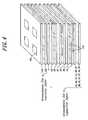
- Figure 4 is a perspective view showing greensheets needed for manufacturing the filter of Figure 3.
- greensheets 15A and 15B for register layers, a greensheet 8 for a joining layer and greensheets 9A to 9R for a capacitor layer are laminated.
- 16A for conductor paste are printed on the greensheet 15A, according to an electrode pattern designed for connection with an outer mounting part or inner conductors.
- 16A for resistor paste are printed on the greensheet 15B, according to a connecting-electrode pattern designed by a distributed constant circuit, or lamped parameter circuit, or the combination thereof.
- Capacitor patterns 14B, designed by a distributed constant circuit, or lamped parameter circuit, or the combination thereof, are printed on the greensheets 9B, 9C, 9D, 9E and 9F for a capacitor layer.
- These greensheets are laminated and heat-pressed to provide laminated greensheets, which are then cut into a predetermined shape to provide a cut body.
- the cut body is sintered at a temperature of 700 to 1100°C and further subjected to barrel polishing.
- Paste for an outer electrode is printed on the surface of the sintered body according to a desired pattern, dried and then fired at a temperature of 500 to 900°C to provide a filter 10 shown in Figure 5.
- the thus obtained filter comprises a resistor layer 11A, a joining layer 4B and a capacitor layer 5B.
- 12 is a connecting electrode pattern and 6B is a capacitor pattern.
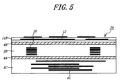
- Figure 5 is a view schematically showing a stacked type LCR filter
- Figure 6 is a perspective view showing greensheets needed for manufacturing the filter of Figure 5.
- greensheets 15C and 15D for register layers As shown in Figure 6, greensheets 15C and 15D for register layers, a greensheet 8 for a joining layer, greensheets 7J, 7K, 7L, 7M, 7N, 7O, 7P, 7Q, 7R and 7S for an inductor layer, another greensheet 8, and greensheets 9S, 9T, 9U, 9V, 9X and 9Y for a capacitor layer are laminated.
- 16B for conductor paste are printed on the outer greensheet 15C, according to an electrode pattern designed for connection with a surface mount part or inner conductors.
- Paste regions for electrodes are printed on the greensheet 15D, according to a coil pattern designed by a distributed constant circuit, or lamped parameter circuit, or the combination thereof.
- Paste regions for electrodes are printed on the greensheets 7L to 7Q for an inductor layer, according to an inductor pattern designed by a distributed constant circuit, or lamped parameter circuit, or the combination thereof.
- Paste regions for electrodes are printed on the greensheets 9U, 9V, 9W and 9X for a capacitor layer, according to a capacitor pattern designed by a distributed constant circuit, or lumped parameter circuit, or the combination thereof.
- These greensheets are laminated and heat-pressed to provide a laminated greensheets, which are then cut into a predetermined shape to provide a cut body.
- the cut body is sintered at a temperature of 700 to 1100°C and further subjected to barrel polishing.
- Paste for an outer electrode is printed on the surface of the sintered body according to a desired pattern, dried and then fired at a temperature of 700 to 1100°C to provide an LCR filter 20 shown in Figure 5.
- the thus obtained filter comprises a resistor layer 11B, joining layers 4A and 4B, an inductor layer 2B and a capacitor layer 5C.
- 12 is a connecting-electrode pattern and 3B is a coil pattern.
- Greensheets shown in Figure 2 were prepared.
- nickel oxide, zinc oxide, copper oxide and ferrous oxide were weighed to a predetermined composition, mixed and calcined to provide a calcined body, which was then granulated to ceramic powder.
- an organic binder, a plasticizer, a dispersing material and solvents, such as xylene and butanol were added, blended and shaped by means of doctor blade method to provide greensheets with a thicknesses of 30 to 200 ⁇ m.
- Paste mainly consisting of silver was printed on some of the greensheets.
- Zinc oxide, barium oxide and titanium oxide were weighed to a predetermined composition as shown in tables 1 and 2, mixed and calcined to provide a calcined body, which was then granulated to ceramic powder.
- ZnO-SiO 2 -B 2 O 3 series glass powder already granulated was added (the content was varied as shown in tables 1 and 2), and an organic binder, a plasticizer, a dispersing material and solvents, such as xylene and butanol, were further added, blended and shaped by means of doctor blade method to provide a greensheet 8 with a thickness of 10 to 1000 ⁇ m.
- Titanium oxide and calcium oxide were weighed to a predetermined composition, mixed and calcined to provide a calcined body, which was then granulated to ceramic powder.
- ZnO-SiO 2 -B 2 O 3 series glass powder already granulated was added, and an organic binder, a plasticizer, a dispersing material and solvents, such as xylene and butanol, were further added, blended and shaped by means of doctor blade method to provide greensheets for a capacitor layer with thicknesses of 10 to 1000 ⁇ m.
- Paste mainly consisting of silver was printed on some of the greensheets.
- each greensheet for a joining layer 8 was observed with eyes. Further, the thus obtained LC filter was embedded within a resin body and polished with the surrounding resin. The amount of warp of each filter was measured with an automated dimension measuring apparatus. The specification for the amount of warp of each sintered filter was not larger than 30 ⁇ m.
- the thickness of the joining layer 4A was also measured on each filter.
- Aluminum rods, for measuring an adhesive strength were adhered and fixed on the surfaces of the magnetic and dielectric layers, respectively, to provide a sample.
- the aluminum rods of each sample were fixed in a tensile strength measuring apparatus to measure its tensile strength.
- the adhesive strength was defined as a value at the moment of fracture.
- LC filters were produced as described in the experiment A, however, manganese oxide or alumina was added to a greensheet for a joining layer.
- the composition of the greensheet was changed as shown in Figure 3, which also shows the experimental results.
- the amount of warp of each filter was considerably decreased according to the invention. Further, when the thickness of the joining layer was adjusted to not smaller than 30 ⁇ m, the amount of warp was considerably lowered and the adhesive strength was considerably improved.
- Greensheets shown in Figure 4 were prepared.
- alumina powder and almino-calcium borosilicate glass were mixed with an organic binder, a plasticizer, a dispersing material and solvents such as xylene and butanol, blended and then shaped by means of doctor blade method to provide greensheets with thicknesses of 0.01 to 1.0 ⁇ m.
- Paste mainly consisting of silver was printed on some of the greensheets.
- Greensheets as shown in Figure 6 were prepared. Greensheets for resistor, joining and capacitor layers were manufactured as described in the experiment E. Greensheets for an inductor layer were also manufactured, as described in the experiment A.
Abstract
Description
- The invention relates to a joining material for an electronic component, such as capacitor, inductors, resistors, stacked type and coaxial type dielectric filters, Stacked type LC filters, composite LC components and composite LCR modules, an electronic component and a method for manufacturing the same.
- When manufacturing a stacked type dielectric filter, a paste for an internal layer electrode is printed on each of a predetermined number of greensheets, which are then laminated to produce laminated greensheets. This laminated greensheets are then sintered at a temperature of 700°C to 1100°C to produce a base body with the internal layer electrodes. After the base body is polished, a metal paste for an outer electrode is printed on predetermined regions on the surface of the body and fired to form the outer electrodes. A composite LC filter with an inductor and capacitor is also known.
- When producing such composite electronic components, a predetermined number of greensheets for, for example, a dielectric layer and magnetic layer are laminated to provide laminated greensheets, which are then co-fired to join the magnetic and dielectric layers. It is also known to provide a greensheet of a joining layer between the greensheets of the magnetic and dielectric layers to provide laminated greensheets which are then co-fired. In Japanese publication Tokkohei 120605/1995, a ceramic material, obtained by firing a mixture of ZnO, TiO2 and CuO, is used for the joining layer for preventing the peeling between the dielectric layers and magnetic layers and diffusion of the ingredients of both layers with each other. In Japanese patent application publication Tokkaihei 36913/1997, a ceramic material is provided between the dielectric and magnetic layers for improving the adhesive strength of the layers and for preventing diffusion of the ingredients of both layers with each other, the ceramic material being obtained by mixing a glass contained in the dielectric layer with a ceramic of 15 to 40 mol% of BaO and 60 to 85 mol% of TiO2 and firing.
- However, according to the inventor's research, warp may occur in the magnetic or dielectric layer depending on the compositions of both layers and their firing schedule. When the amount of warp is out of the specification for manufacturing a filter, such filter with impermissible warp is discarded as a defective, thus decreasing its manufacturing yield. The inventors further found that warp was also induced in the layers during sintering process.
- The object of the invention is, in an electronic component having a plurality of functional layers each selected from a magnetic layer and dielectric layer and joined with each other, to prevent warp in the magnetic layers or the dielectric layer.
- The invention provides a joining material for an electronic component having a plurality of functional layers each selected from a magnetic layer and dielectric layer, the functional layers being joined with the joining material with each other, the joining material comprising a glass and a composition of a mol% of ZnO, b mol% of BaO and c mol% of TiO2 (a=12-45, b=4-45, c=18-81,
- The invention also provides a joining material for the electric component, the joining material comprising a glass and a composition of a mol% of ZnO, b mol% of BaO, c mol% of TiO2 and d mol% of MnO (a=12-45, b=4-45, c=18-81, d≤10,
- The invention also provides a joining material for the electric component, the joining material comprising a glass and a composition of a mol% of ZnO, b mol% of BaO, c mol% of TiO2, and e mol% of Al2O3 (a=12-45, b=4-45, c=18-81, e≤10,
- The invention also provides a joining material for the electric component, the joining material comprising a glass and a composition of a mol% of ZnO, b mol% of BaO, c mol% of TiO2, d mol% of MnO and e mol% of A12O3 (a=12-45, b=4-45, c=18-81, d≤10,e≤10,
- The invention may be stated as providing a joining material suitable for joining functional layers of an electronic component, which joining material is composed of a glass and a composition containing from 12 to 45 mol% of ZnO, from 4-45 mol% of BaO, from 18-81 mol% of TiO2 and optionally upto 40 mol% of other metal oxides, preferably not more than 30, 20 or even not more than 10 mol% of other metal oxides. Preferences for these other metal oxides are not more than 10% of manganese oxide and/or not more than 10% of Al2O3, and not more than 10% of a metal oxide which is Y203, ZrO2 or a mixture of them, and/or not more than 10% of a metal oxide selected from a group consisting of Cr203, Fe203 and NiO and mixtures of them.
- The invention also provides a method of making a joining material by mixing a said composition of metal oxides and a glass in proportions of 0.1-10 weight parts of the glass per 100 weight parts of the composition.
- The invention also provides an electronic component having the functional layers and a joining layer for joining the adjacent functional layers, wherein the joining layer is composed of sintered product of each of the joining materials. That is, a layer composed of each of the joining materials is fired to form the joining layer. The joining layer is made of the sintered product obtained by firing the joining material.
- The invention also provides an electronic component having the functional layers and a joining layer, wherein the joining layer is composed of sintered product showing at least one of a peak corresponding to BaNd2Ti5O14 and a peak corresponding to BaNd2Ti4O12 when measured by means of powdery X-ray diffraction method.
- The invention also provides a method for manufacturing an electronic component having the functional layers and a joining layer, the method comprising the steps of:
- laminating the functional layers already sintered to provide a laminated body, wherein a layer made of each of the joining materials is provided, and
- firing the joining material to form the joining layer.
-
- The invention also provides a method for manufacturing an electronic component having the functional layers and a joining layer, the method comprising the steps of:
- laminating greensheets, for the functional layers, to provide laminated greensheets, wherein a layer made of each of the joining materials is provided, and
- firing the laminated greensheets with the layer made of the joining material to form the functional layers and the joining layer.
-
- The inventors researched the above described warp of a dielectric layer or magnetic layer and finally made the following discovery. According to state-of-the-art knowledge, it is possible to improve the adhesive strength and therefore to prevent the peeling of the magnetic and dielectric layers, by adjusting the thermal expansion coefficient of joining ceramics between the magnetic and dielectric layers to those of both layers.
- However, in actual manufacturing process, depending on the selection of materials for the magnetic and dielectric layers and sintering schedule, even when the thermal coefficient of the joining ceramics is adjusted to those of the magnetic and dielectric layers, warp may be observed during the sintering process. This phenomenon probably means that the magnetic, dielectric and joining layers shrink at different firing shrinkage rates at certain or even almost any time point during the sintering.
- The inventors, based on the above discovery, successfully provide a solution. That is, the above warp may be considerably decreased or even prevented, on a wide variety of materials for magnetic and dielectric layers, by providing a joining material of each of the above specific compositions.
- In the above compositions, for further reducing the warp of the magnetic or dielectric layer, a content of ZnO (a mol%) may preferably be 25 to 40 mol%, a content of BaO (b mol%) may preferably be 5 to 15 mol%, and a content of TiO2 (c mol%) may preferably be 45 to 65 mol%.
- A glass contained in the inventive joining material may preferably be selected from a group consisting of ZnO-SiO2-B2O3 glass, PbO-B2O3-SiO2 glass, Al2O3-CaO-B2O3-SiO2 glass, B2O3-SiO2 glass, MgO-Al2O3-SiO2 cordierite glass, and ZnO-MgO-Al2O3-SiO2 cordierite glass, and most preferably be ZnO-SiO2-B2O3 glass. These glasses may further contain TiO2, ZrO2 or Y2O3.
- The greensheets for the inventive joining layer may be made brown, by adding not more than 10 mol% of MnO to the inventive joining material, to distinguish the brown-colored greensheet from greensheets for magnetic and dielectric layers. The joining layer may also be colored by adding at least one metal oxide selected from a group consisting of Cr2O3, Fe2O3 and NiO.
- Not more than 10 mol% of Al2O3 may be added to the inventive joining material to further improve the adhesive strength of functional layers. Not more than 10 mol% of at least one metal oxide selected form a group consisting of Y2O3 and ZrO2 may be also added to the inventive joining material to further improve the adhesive strength of adjacent functional layers.
- More than 10 mol% of MnO added to the joining material might reduce the adhesive strength between the functional layers. More than 10 mol% of Al2O3 added to the joining material might increase the warp of functional layers.
- In the invention, at least one of the functional layers functions as an element in an equivalent circuit, and therefore functions as an electronic device layer. Such electronic device layer includes inductor, capacitor and resistor layers. The inductor layer may preferably comprises a magnetic layer and an inductor, such as a coil, as a conductor embedded within the magnetic layer. The capacitor layer may preferably comprises a dielectric layer and a capacitor as a conductor embedded within the dielectric layer. The magnetic layer means a layer made of a magnetic material, in the invention.
- The invention is particularly suitable for a composite electronic component, preferably being an LC filter, stacked type dielectric filter or an LCR integrated substrate.
- The dielectric layer may be preferably made of a TiO2, TiO2 CaO, BaO-TiO2, BaO-TiO2-Nd2O3, BaO-TiO2-Nd2O3-Bi2O3, BaO TiO2-ZnO, BaO-Al2O3-SiO2, MgO-CaO-TiO2, BaO-MgO-Ta2O5 or Al2O3 series oxide. Such oxide may include a glass, which is preferably selected from B2O3-SiO2, CaO-B2O3-SiO2, CaO-Al2O3-B2O3-SiO2 and CaO-Al2O3-TiO2-SiO2 series glasses.
- The magnetic layer may preferably be made of a Fe2O3-NiO-CuO-ZnO, Fe2O3-NiO-CuO-ZnO-SiO2, NiO-ZnO, or CuO-ZnO or feroux planar series oxide. These magnetic material may contain not more than 5 weight percent of CoO or MnO, and about 1 weight percent of SiO, CaO, PbO, or Bi2O3 constituting a glass. When applying these materials, warp may be induced more often, thus increasing the need for the invention.
- When the joining layer has a thickness of not smaller than 10µm, an amount of warp may be considerably reduced and the tensile strength thereof may be improved. The upper limit of the thickness is not particularly mentioned, however, the layer with a thickness of not larger than 500 µm is practical.
-
- Figure 1 is a view schematically showing an LC filter suitable for applying the invention,
- Figure 2 is a perspective view showing greensheets needed for manufacturing the filter of Figure 1,
- Figure 3 is a view schematically showing a stacked type dielectric filter suitable for applying the invention,
- Figure 4 is a perspective view showing greensheets needed for manufacturing the filter of Figure 3,
- Figure 5 is a view schematically showing a stacked type LCR filter suitable for applying the invention,
- Figure 6 is a perspective view showing greensheets needed for manufacturing the filter of Figure 5,
- Figure 7 is a photograph showing a polished surface of the filter sintered according to experimental number 16 within the invention, and
- Figure 8 is a photograph showing a polished surface of the filter sintered according to control experimental number 19 outside of the invention.
-
- Figure 1 is a view schematically showing an LC filter, and Figure 2 is a perspective view needed for manufacturing an LC filter of Figure 1.
- As shown in Figure 2,
greensheets greensheet 8 for a joining layer, andgreensheets greensheets 7B to 7H for inductor layers, according to a coil pattern designed by a lumped parameter circuit. 14A for conductor paste are printed on the greensheets for a capacitor layer, according to a capacitor pattern designed by a lumped parameter circuit. - These greensheets are laminated and heat-pressed to provide laminated greensheets, which are then cut into a predetermined shape to provide a cut body. The cut body is sintered at a temperature of 800 to 950°C and further subjected to barrel polishing. Paste for an outer electrode is printed on the surface of the sintered body according to a predetermined pattern, dried and then fired at a temperature of 500 to 850°C to provide an LC filter shown in Figure 1. The thus obtained LC filter comprises an
inductor layer 2A, a joininglayer 4A and acapacitor layer 5A. 3A is a coil pattern and 6A is a capacitor pattern. - Figure 3 is a view schematically showing a stacked type dielectric filter, and Figure 4 is a perspective view showing greensheets needed for manufacturing the filter of Figure 3.
- As shown in Figure 4, greensheets 15A and 15B for register layers, a
greensheet 8 for a joining layer andgreensheets 9A to 9R for a capacitor layer are laminated. 16A for conductor paste are printed on the greensheet 15A, according to an electrode pattern designed for connection with an outer mounting part or inner conductors. 16A for resistor paste are printed on thegreensheet 15B, according to a connecting-electrode pattern designed by a distributed constant circuit, or lamped parameter circuit, or the combination thereof.Capacitor patterns 14B, designed by a distributed constant circuit, or lamped parameter circuit, or the combination thereof, are printed on thegreensheets - These greensheets are laminated and heat-pressed to provide laminated greensheets, which are then cut into a predetermined shape to provide a cut body. The cut body is sintered at a temperature of 700 to 1100°C and further subjected to barrel polishing. Paste for an outer electrode is printed on the surface of the sintered body according to a desired pattern, dried and then fired at a temperature of 500 to 900°C to provide a
filter 10 shown in Figure 5. The thus obtained filter comprises aresistor layer 11A, a joininglayer 4B and a capacitor layer 5B. 12 is a connecting electrode pattern and 6B is a capacitor pattern. - Figure 5 is a view schematically showing a stacked type LCR filter, and Figure 6 is a perspective view showing greensheets needed for manufacturing the filter of Figure 5.
- As shown in Figure 6, greensheets 15C and 15D for register layers, a
greensheet 8 for a joining layer,greensheets greensheet 8, andgreensheets greensheet 15D, according to a coil pattern designed by a distributed constant circuit, or lamped parameter circuit, or the combination thereof. Paste regions for electrodes are printed on thegreensheets 7L to 7Q for an inductor layer, according to an inductor pattern designed by a distributed constant circuit, or lamped parameter circuit, or the combination thereof. Paste regions for electrodes are printed on thegreensheets - These greensheets are laminated and heat-pressed to provide a laminated greensheets, which are then cut into a predetermined shape to provide a cut body. The cut body is sintered at a temperature of 700 to 1100°C and further subjected to barrel polishing. Paste for an outer electrode is printed on the surface of the sintered body according to a desired pattern, dried and then fired at a temperature of 700 to 1100°C to provide an
LCR filter 20 shown in Figure 5. The thus obtained filter comprises aresistor layer 11B, joininglayers inductor layer 2B and a capacitor layer 5C. 12 is a connecting-electrode pattern and 3B is a coil pattern. - Greensheets shown in Figure 2 were prepared. For greensheets for an inductor layer, nickel oxide, zinc oxide, copper oxide and ferrous oxide were weighed to a predetermined composition, mixed and calcined to provide a calcined body, which was then granulated to ceramic powder. To the ceramic powder, an organic binder, a plasticizer, a dispersing material and solvents, such as xylene and butanol, were added, blended and shaped by means of doctor blade method to provide greensheets with a thicknesses of 30 to 200 µm. Paste mainly consisting of silver was printed on some of the greensheets.
- Zinc oxide, barium oxide and titanium oxide were weighed to a predetermined composition as shown in tables 1 and 2, mixed and calcined to provide a calcined body, which was then granulated to ceramic powder. To the ceramic powder, ZnO-SiO2-B2O3 series glass powder already granulated was added (the content was varied as shown in tables 1 and 2), and an organic binder, a plasticizer, a dispersing material and solvents, such as xylene and butanol, were further added, blended and shaped by means of doctor blade method to provide a
greensheet 8 with a thickness of 10 to 1000 µm. - Titanium oxide and calcium oxide were weighed to a predetermined composition, mixed and calcined to provide a calcined body, which was then granulated to ceramic powder. To the ceramic powder, ZnO-SiO2-B2O3 series glass powder already granulated was added, and an organic binder, a plasticizer, a dispersing material and solvents, such as xylene and butanol, were further added, blended and shaped by means of doctor blade method to provide greensheets for a capacitor layer with thicknesses of 10 to 1000 µm. Paste mainly consisting of silver was printed on some of the greensheets.
- These greensheets were laminated, heat-pressed and cut into a predetermined shape to provide a cut body, which was then sintered at a temperature of not higher than 1100°C. Paste mainly consisting of silver was printed on the thus obtained sintered body according to an outer electrode pattern and fired to provide an LC filter.
- The color of each greensheet for a joining
layer 8 was observed with eyes. Further, the thus obtained LC filter was embedded within a resin body and polished with the surrounding resin. The amount of warp of each filter was measured with an automated dimension measuring apparatus. The specification for the amount of warp of each sintered filter was not larger than 30 µm. - The thickness of the joining
layer 4A was also measured on each filter. Aluminum rods, for measuring an adhesive strength, were adhered and fixed on the surfaces of the magnetic and dielectric layers, respectively, to provide a sample. The aluminum rods of each sample were fixed in a tensile strength measuring apparatus to measure its tensile strength. The adhesive strength was defined as a value at the moment of fracture. These experimental results were shown in tables 1 and 2.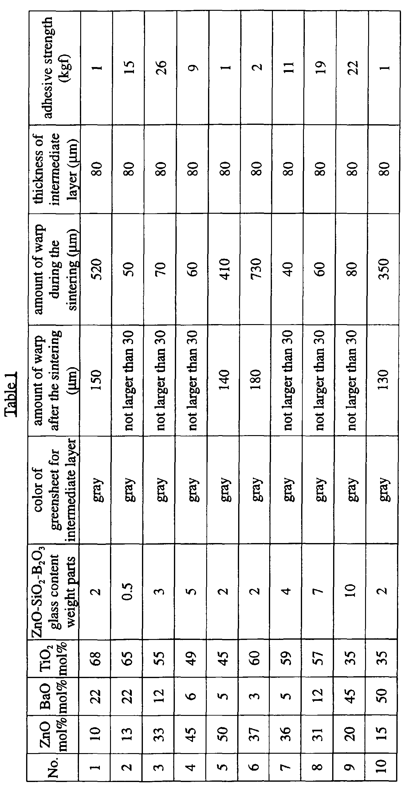

- As can be seen from the results, when adjusting a content of zinc oxide to 12 to 45 mol%, a content of barium oxide to 4 to 45 mol%, a content of TiO2 to 18 to 81 mol% and a content of ZnO-SiO2-B2O3 series glass to 0.5 to 10 weight parts, the amount of warp was considerably decreased to not high than 30 µm.
- X-ray diffraction curve was measured on each sample of experimental numbers of 2, 3, 4, 7, 8, 9, 12, 13, 14, 16, 17 and 18 shown in tables 1 and 2. Consequently, either of or both peaks corresponding to BaNd2Ti5O14 and BaNd2Ti4O12 was found.
- Then, when the above cut bodies of experimental numbers 16 and 19 before the sintering were subjected to the sintering, each body's appearance was observed by means of a heating microscope to take a photograph showing the dielectric layer, magnetic layer and joining layer. In the filter of the number 16 fallen within the invention, the amount of warp of each functional layer was up to 30 µm. On the contrary, in the filter of the control experimental number 19, the amount of warp of the whole filter was more than 1000 µm.
- LC filters were produced as described in the experiment A, however, manganese oxide or alumina was added to a greensheet for a joining layer. The composition of the greensheet was changed as shown in Figure 3, which also shows the experimental results.

- Consequently, same as the experiment A, when adjusting a content of zinc oxide to 12 to 45 mol%, a content of barium oxide to 4 to 45 mol%, a content of TiO2 to 18 to 81 mol% and a content of ZnO-SiO2-B2O3 series glass to 0.1 to 10 weight parts, the amount of warp of each filter was decreased to not higher than 80 µm during the sintering, and to not higher than 30 µm after the sintering. Further, the greensheet was colored brown by adding MnO. However, when MnO was added in an amount of more than 10 mol%, the adhesive strength was lowered.
- Although the addition of alumina increased considerably the adhesive strength, when alumina was added in an amount of more than 10 mol%, the amount of warp of the filter after the sintering was more than 70 µm.
- LC filters were manufactured as described in the experiment A, however, the compositions of the greensheets for joining layers were changed as shown in table 4, showing the experimental results.

- Consequently, same as the experiment A, when adjusting contents of zinc oxide, barium oxide, titanium oxide, manganese oxide and alumina according to the invention and a content of ZnO-SiO2-B2O3 series glass to 0.1 to 10 weight parts, the amount of warp of each filter was considerably decreased during the sintering. When the amount of the glass was out of a range of 0.1 to 10 weight parts, the amount of warp was more than 70 µm.
- LC filters were manufactured as described in the experiment A, however, the compositions of the greensheets for joining layers were adjusted in the preferred range of the invention and thicknesses of the joining layers were changed. The results were shown in table 5.

- Consequently, same as the experiment A, the amount of warp of each filter was considerably decreased according to the invention. Further, when the thickness of the joining layer was adjusted to not smaller than 30 µm, the amount of warp was considerably lowered and the adhesive strength was considerably improved.
- Greensheets shown in Figure 4 were prepared. In greensheets for a resistor layer, alumina powder and almino-calcium borosilicate glass were mixed with an organic binder, a plasticizer, a dispersing material and solvents such as xylene and butanol, blended and then shaped by means of doctor blade method to provide greensheets with thicknesses of 0.01 to 1.0 µm. Paste mainly consisting of silver was printed on some of the greensheets.
- 33 mol% of Zinc oxide, 12 mol% of barium oxide and 55 mol% of titanium oxide were weighed, mixed and calcined to provide a calcined body, which was then granulated to ceramic powder. To the ceramic powder, 2 weight parts of ZnO-SiO2-B2O3 series glass powder already granulated was added, and an organic binder, a plasticizer, a dispersing material and solvents, such as xylene and butanol, were further added, blended and shaped by means of doctor blade method to provide a
greensheet 8 with a thickness of 10 to 1000 µm, - Barium oxide, titanium oxide, neodymium oxide and bismuth oxide were weighed, mixed and calcined to provide a calcined body, which was then granulated to ceramic powder. To the ceramic powder, an organic binder, a plasticizer, a dispersing material and solvents, such as xylene and butanol, were further added, blended and shaped by means of doctor blade method to provide greensheets for a capacitor layer with thicknesses of 10 to 500 µm. Paste mainly consisting of silver was printed on some of the greensheets.
- These greensheets were laminated and heat-pressed to provide a laminated body, which was then cut into a cut body with a pre-determined shape. The cut body was sintered at a temperature of not higher than 1100°C to obtain a stacked type dielectric filter, whose amount of warp was found to be not larger than 30 µm.
- Greensheets as shown in Figure 6 were prepared. Greensheets for resistor, joining and capacitor layers were manufactured as described in the experiment E. Greensheets for an inductor layer were also manufactured, as described in the experiment A.
- These greensheets were laminated and heat-pressed to provide a laminated body, which was then cut into a cut body with a pre-determined shape. The cut body was then sintered at a temperature not higher than 1100°C to obtain an LCR filter, whose amount of warp was found to be not large than 30 µm.
Claims (14)
- A joining material for an electronic component having a plurality of functional layers each selected from a magnetic layer and dielectric layer, the functional layers being joined with each other by means of the joining material, the joining material comprising a glass and a composition of a mol% of ZnO, b mol% of BaO and c mol% of TiO2 (a=12-45, b=4-45, c=18-81,
- A joining material for an electronic component having a plurality of functional layers each selected from a magnetic layer and dielectric layer, the functional layers being joined with each other by means of the joining material, the joining material comprising a glass and a composition of a mol% of ZnO, b mol% of BaO, c mol% of TiO2 and d mol% of MnO (a=12-45, b=4-45, c=18-81, d≤10,
- A joining material for an electronic component having a plurality of functional layers each selected from a magnetic layer and dielectric layer, the functional layers being joined with each other by means of the joining material, the joining material comprising a glass and a composition of a mol% of ZnO, b mol% of BaO, c mol% of TiO2 and e mol% of Al2O3 (a=12-45, b=4-45, c=18-81, e≤10,
- A joining material for an electronic component having a plurality of functional layers each selected from a magnetic layer and dielectric layer, the functional layers being joined with each other by means of the joining material, the joining material comprising a glass and a composition of a mol% of ZnO, b mol% of BaO, c mol% of TiO2, d mol% of MnO and e mol% of Al2O3 (a=12-45, b=4-45, c=18-81 d≤10, e≤10,
- The joining material as claimed in any of claims 1 to 4, wherein a content of ZnO is 25 to 40 mol%, a content of BaO is 5 to 15 mol% and a content of TiO2 is 45 to 65 mol%.
- The joining material as claimed in any of claims 1 to 5, further comprising not more than 10 mol% of at least one metal oxide selected from a group consisting of Cr2O3, Fe2O3 and NiO.
- The joining material as claimed in any of claims 1 to 5, further comprising not more than 10 mol% of at least one metal oxide selected from a group consisting of Y2O3 and ZrO2.
- The joining material for an electronic component as claimed in any of claims 1 to 7, wherein the glass is selected from a group consisting of ZnO-SiO2-B2O3 glass, PbO-B2O3-SiO2 glass, Al2O3-CaO-B2O3-SiO2 glass, B2O3-SiO2 glass, MgO-Al2O3-SiO2 cordierite glass, and ZnO-MgO-Al2O3-SiO2 cordierite glass.
- An electronic component having a plurality of functional layers each selected from a magnetic layer and dielectric layer and a joining layer, wherein the joining layer is composed of sintered product of the joining material as claimed in any of claims 1 to 8.
- An electronic component having a plurality of functional layers each selected from a magnetic layer and dielectric layer and a joining layer, wherein the joining layer is composed of sintered product showing at least one of a peak corresponding to BaNd2Ti5O14 and a peak corresponding to BaNd2Ti4O12, when measured by means of powdery X-ray diffraction method.
- The electronic component as claimed in claim 9 or 10, wherein the joining layer has a thickness of not smaller than 10µm and not larger than 500µm.
- A method for manufacturing an electronic component having a plurality of functional layers each selected from a magnetic layer and dielectric layer, together with at least one joining layer, the method comprising the steps of:laminating sintered functional layers to provide a laminated body, with a layer made of the joining material as claimed in any one of claims 1 to 8 provided between the functional layers, andfiring the joining material to form the joining layer.
- A method for manufacturing an electronic component having a plurality of functional layers each selected from a magnetic layer and dielectric layer together with at least one joining layer, the method comprising the steps of:laminating greensheets for the functional layers, to provide laminated greensheets, wherein a layer made of the joining material as claimed in any of claims 1 to 8 is provided between the functional layers, andfiring the laminated greensheets with the layer(s) made of the joining material to form the functional layers and the joining layer(s).
- The method as claimed in claim 12 or 13, wherein the layer made of the joining material is provided as a form of a greensheet, paste, slurry, or thin film.
Applications Claiming Priority (2)
| Application Number | Priority Date | Filing Date | Title |
|---|---|---|---|
| JP5910898 | 1998-02-25 | ||
| JP05910898A JP4257711B2 (en) | 1998-02-25 | 1998-02-25 | Bonding agent for electronic parts and electronic parts |
Publications (2)
| Publication Number | Publication Date |
|---|---|
| EP0939061A1 true EP0939061A1 (en) | 1999-09-01 |
| EP0939061B1 EP0939061B1 (en) | 2003-06-04 |
Family
ID=13103798
Family Applications (1)
| Application Number | Title | Priority Date | Filing Date |
|---|---|---|---|
| EP99301394A Expired - Lifetime EP0939061B1 (en) | 1998-02-25 | 1999-02-25 | Joining material for electronic components, electronic components and a method for manufacturing the same |
Country Status (4)
| Country | Link |
|---|---|
| US (2) | US6376085B1 (en) |
| EP (1) | EP0939061B1 (en) |
| JP (1) | JP4257711B2 (en) |
| DE (1) | DE69908445T2 (en) |
Cited By (4)
| Publication number | Priority date | Publication date | Assignee | Title |
|---|---|---|---|---|
| US6582807B2 (en) * | 2000-04-07 | 2003-06-24 | Case Western Reserve University | Polymer 1D photonic crystals |
| WO2009043826A1 (en) * | 2007-09-28 | 2009-04-09 | Epcos Ag | Electrical multilayer component and method for producing an electrical multilayer component |
| EP2194766A1 (en) * | 2007-09-28 | 2010-06-09 | Soshin Electric Co. Ltd. | Ceramic multilayer substrate |
| EP3919463A1 (en) * | 2020-06-02 | 2021-12-08 | Heraeus GMSI LLC | Plasma resistant ceramic body formed from multiple pieces |
Families Citing this family (20)
| Publication number | Priority date | Publication date | Assignee | Title |
|---|---|---|---|---|
| JP3635631B2 (en) * | 1999-12-20 | 2005-04-06 | 株式会社村田製作所 | Manufacturing method of multilayer ceramic electronic component |
| US7160176B2 (en) * | 2000-08-30 | 2007-01-09 | Micron Technology, Inc. | Methods and apparatus for electrically and/or chemically-mechanically removing conductive material from a microelectronic substrate |
| DE10313891A1 (en) * | 2003-03-27 | 2004-10-14 | Epcos Ag | Electrical multilayer component |
| JP4619026B2 (en) * | 2003-10-24 | 2011-01-26 | 京セラ株式会社 | Glass ceramic substrate and manufacturing method thereof |
| WO2005087492A1 (en) * | 2004-02-13 | 2005-09-22 | The Procter & Gamble Company | Discoloration-resistant articles for applying color on surfaces and methods of reducing discoloration in articles for applying color on surfaces |
| JP4746423B2 (en) * | 2005-12-22 | 2011-08-10 | 日本特殊陶業株式会社 | Wiring board built-in capacitor manufacturing method and wiring board built-in capacitor |
| JP2007242986A (en) * | 2006-03-10 | 2007-09-20 | Tdk Corp | Bonding interlayer and composite multilayer electronic component |
| JP2008289111A (en) * | 2007-04-19 | 2008-11-27 | Tdk Corp | Multilayer filter |
| US7728695B2 (en) | 2007-04-19 | 2010-06-01 | Tdk Corporation | Multilayer filter having an inductor portion and a varistor portion stacked with an intermediate portion |
| DE102007020783A1 (en) * | 2007-05-03 | 2008-11-06 | Epcos Ag | Electrical multilayer component |
| DE102007031510A1 (en) * | 2007-07-06 | 2009-01-08 | Epcos Ag | Electrical multilayer component |
| JP5428315B2 (en) * | 2008-12-11 | 2014-02-26 | 株式会社村田製作所 | Electronic components |
| JP2010226038A (en) * | 2009-03-25 | 2010-10-07 | Tdk Corp | Ceramic electronic component |
| JP5152308B2 (en) * | 2010-03-09 | 2013-02-27 | Tdk株式会社 | Ceramic electronic components |
| JP5120406B2 (en) * | 2010-03-31 | 2013-01-16 | Tdk株式会社 | Ceramic electronic component and method for manufacturing ceramic electronic component |
| JP6005945B2 (en) * | 2011-03-18 | 2016-10-12 | 日本碍子株式会社 | Composite electronic components |
| KR20160076638A (en) * | 2014-12-23 | 2016-07-01 | 삼성전기주식회사 | Composite electronic component and board for mounting the same |
| JP6231050B2 (en) | 2015-07-21 | 2017-11-15 | Tdk株式会社 | Composite electronic components |
| JP7252702B2 (en) * | 2017-06-06 | 2023-04-05 | 太陽誘電株式会社 | Composite electronic component, composite electronic component package, and circuit board |
| US20230212082A1 (en) * | 2020-05-26 | 2023-07-06 | Heraeus Conamic North America Llc | Plasma resistant ceramic body formed from multiple pieces |
Citations (4)
| Publication number | Priority date | Publication date | Assignee | Title |
|---|---|---|---|---|
| US4610969A (en) * | 1983-11-30 | 1986-09-09 | Taiyo Yuden Co., Ltd. | Low temperature sintered ceramic material for use in solid dielectric capacitors or the like, and method of manufacture |
| US4772985A (en) * | 1986-09-24 | 1988-09-20 | Kabushiki Kaisha Toshiba | Thick film capacitor |
| US4882650A (en) * | 1988-12-05 | 1989-11-21 | Sprague Electric Company | Magnesium titanate ceramic and dual dielectric substrate using same |
| EP0533162A1 (en) * | 1991-09-18 | 1993-03-24 | Ngk Spark Plug Co., Ltd | BaO-xTiO2 dielectric ceramic composition |
Family Cites Families (2)
| Publication number | Priority date | Publication date | Assignee | Title |
|---|---|---|---|---|
| JP3796663B2 (en) | 1993-10-26 | 2006-07-12 | ミネベア株式会社 | Planar light source device and manufacturing method thereof |
| JPH0836913A (en) | 1994-07-25 | 1996-02-06 | Toto Ltd | Light bulb fixing device and socket for fixing light bulb |
-
1998
- 1998-02-25 JP JP05910898A patent/JP4257711B2/en not_active Expired - Fee Related
-
1999
- 1999-02-24 US US09/256,856 patent/US6376085B1/en not_active Expired - Fee Related
- 1999-02-25 EP EP99301394A patent/EP0939061B1/en not_active Expired - Lifetime
- 1999-02-25 DE DE69908445T patent/DE69908445T2/en not_active Expired - Lifetime
-
2001
- 2001-10-31 US US10/001,677 patent/US20020064669A1/en not_active Abandoned
Patent Citations (4)
| Publication number | Priority date | Publication date | Assignee | Title |
|---|---|---|---|---|
| US4610969A (en) * | 1983-11-30 | 1986-09-09 | Taiyo Yuden Co., Ltd. | Low temperature sintered ceramic material for use in solid dielectric capacitors or the like, and method of manufacture |
| US4772985A (en) * | 1986-09-24 | 1988-09-20 | Kabushiki Kaisha Toshiba | Thick film capacitor |
| US4882650A (en) * | 1988-12-05 | 1989-11-21 | Sprague Electric Company | Magnesium titanate ceramic and dual dielectric substrate using same |
| EP0533162A1 (en) * | 1991-09-18 | 1993-03-24 | Ngk Spark Plug Co., Ltd | BaO-xTiO2 dielectric ceramic composition |
Cited By (9)
| Publication number | Priority date | Publication date | Assignee | Title |
|---|---|---|---|---|
| US6582807B2 (en) * | 2000-04-07 | 2003-06-24 | Case Western Reserve University | Polymer 1D photonic crystals |
| US6696142B2 (en) * | 2000-04-07 | 2004-02-24 | Case Western Reserve University | Polymer 1D photonic crystals |
| WO2009043826A1 (en) * | 2007-09-28 | 2009-04-09 | Epcos Ag | Electrical multilayer component and method for producing an electrical multilayer component |
| EP2194766A1 (en) * | 2007-09-28 | 2010-06-09 | Soshin Electric Co. Ltd. | Ceramic multilayer substrate |
| US8134447B2 (en) | 2007-09-28 | 2012-03-13 | Epcos Ag | Electrical multilayer component and method for producing an electrical multilayer component |
| EP2530690A1 (en) * | 2007-09-28 | 2012-12-05 | Epcos Ag | Electric multi-layer element and method for producing an electric multi-layer element |
| EP2530689A1 (en) * | 2007-09-28 | 2012-12-05 | Epcos Ag | Electrical multilayer component and method for producing an electrical multilayer component |
| EP2194766A4 (en) * | 2007-09-28 | 2013-08-21 | Soshin Electric | Ceramic multilayer substrate |
| EP3919463A1 (en) * | 2020-06-02 | 2021-12-08 | Heraeus GMSI LLC | Plasma resistant ceramic body formed from multiple pieces |
Also Published As
| Publication number | Publication date |
|---|---|
| JPH11243034A (en) | 1999-09-07 |
| JP4257711B2 (en) | 2009-04-22 |
| DE69908445D1 (en) | 2003-07-10 |
| US20020064669A1 (en) | 2002-05-30 |
| EP0939061B1 (en) | 2003-06-04 |
| DE69908445T2 (en) | 2004-05-06 |
| US6376085B1 (en) | 2002-04-23 |
Similar Documents
| Publication | Publication Date | Title |
|---|---|---|
| EP0939061B1 (en) | Joining material for electronic components, electronic components and a method for manufacturing the same | |
| CA1301867C (en) | Multilayered ceramic capacitor and manufacturing thereof | |
| EP0916630B1 (en) | Nonmagnetic ceramic and laminated ceramic parts | |
| KR100363655B1 (en) | Dielectric ceramic component and ceramic electronic parts using the same | |
| EP2397452A1 (en) | Sintered body of low temperature cofired ceramic and multilayer ceramic substrate | |
| DE10002812A1 (en) | Low firing temperature ceramic composition, e.g. for producing dielectric ceramics and multilayer ceramic substrates, is prepared by mixing borosilicate glass with a calcined copper oxide and barium-bismuth-lanthanide titanate mixture | |
| EP0474354B1 (en) | Dielectric ceramic body, method of producing the same and circuit board using the same | |
| US5990028A (en) | Dielectric paste | |
| EP2234128A1 (en) | Ceramic Electronic Component | |
| CN107921744A (en) | Layered product and electronic unit | |
| EP0960866B1 (en) | Ceramic substrate composition and ceramic circuit component | |
| EP0843410B1 (en) | Inductance-capacitance composite component | |
| EP2330604A1 (en) | Composite electronic component | |
| KR100373943B1 (en) | Magnetic Dielectric Ceramic Composites, Manufacturing Method and Usage thereof, and Multifunctional Device | |
| JP2001010858A (en) | Composition for ceramic substrate and ceramic circuit part | |
| JP2001244140A (en) | Ceramic laminate and manufacturing method thereof, electronic component and electronic device | |
| EP1130003A1 (en) | Glass ceramics composition and electronic parts and multilayered lc multiple component using the same | |
| JP4587758B2 (en) | Glass ceramic substrate | |
| EP1022264A2 (en) | Low temperature-fired porcelain articles and electronic parts including such porcelain articles | |
| EP1462426A1 (en) | Low temperature co-fired ferrite-ceramic composite and the process for manufacturing it | |
| JP2000211969A (en) | Porcelain fired at lower temperature and electronic parts equipped therewith | |
| JP3917770B2 (en) | Low-temperature fired porcelain and electronic component equipped with the same | |
| JP3645046B2 (en) | Non-magnetic ceramic and ceramic laminated parts | |
| JP2006156499A (en) | Multiple-pattern substrate and glass ceramic board | |
| JP2002324730A (en) | Laminated ceramic electronic component and its manufacturing method |
Legal Events
| Date | Code | Title | Description |
|---|---|---|---|
| PUAI | Public reference made under article 153(3) epc to a published international application that has entered the european phase |
Free format text: ORIGINAL CODE: 0009012 |
|
| AK | Designated contracting states |
Kind code of ref document: A1 Designated state(s): DE FR GB |
|
| AX | Request for extension of the european patent |
Free format text: AL;LT;LV;MK;RO;SI |
|
| 17P | Request for examination filed |
Effective date: 20000107 |
|
| AKX | Designation fees paid |
Free format text: DE FR GB |
|
| 17Q | First examination report despatched |
Effective date: 20020306 |
|
| GRAH | Despatch of communication of intention to grant a patent |
Free format text: ORIGINAL CODE: EPIDOS IGRA |
|
| GRAH | Despatch of communication of intention to grant a patent |
Free format text: ORIGINAL CODE: EPIDOS IGRA |
|
| GRAA | (expected) grant |
Free format text: ORIGINAL CODE: 0009210 |
|
| AK | Designated contracting states |
Designated state(s): DE FR GB |
|
| REG | Reference to a national code |
Ref country code: GB Ref legal event code: FG4D |
|
| REF | Corresponds to: |
Ref document number: 69908445 Country of ref document: DE Date of ref document: 20030710 Kind code of ref document: P |
|
| PLBE | No opposition filed within time limit |
Free format text: ORIGINAL CODE: 0009261 |
|
| STAA | Information on the status of an ep patent application or granted ep patent |
Free format text: STATUS: NO OPPOSITION FILED WITHIN TIME LIMIT |
|
| ET | Fr: translation filed | ||
| 26N | No opposition filed |
Effective date: 20040305 |
|
| PGFP | Annual fee paid to national office [announced via postgrant information from national office to epo] |
Ref country code: FR Payment date: 20140211 Year of fee payment: 16 |
|
| PGFP | Annual fee paid to national office [announced via postgrant information from national office to epo] |
Ref country code: GB Payment date: 20140219 Year of fee payment: 16 |
|
| PGFP | Annual fee paid to national office [announced via postgrant information from national office to epo] |
Ref country code: DE Payment date: 20140417 Year of fee payment: 16 |
|
| REG | Reference to a national code |
Ref country code: DE Ref legal event code: R119 Ref document number: 69908445 Country of ref document: DE |
|
| GBPC | Gb: european patent ceased through non-payment of renewal fee |
Effective date: 20150225 |
|
| REG | Reference to a national code |
Ref country code: FR Ref legal event code: ST Effective date: 20151030 |
|
| PG25 | Lapsed in a contracting state [announced via postgrant information from national office to epo] |
Ref country code: DE Free format text: LAPSE BECAUSE OF NON-PAYMENT OF DUE FEES Effective date: 20150901 Ref country code: GB Free format text: LAPSE BECAUSE OF NON-PAYMENT OF DUE FEES Effective date: 20150225 |
|
| PG25 | Lapsed in a contracting state [announced via postgrant information from national office to epo] |
Ref country code: FR Free format text: LAPSE BECAUSE OF NON-PAYMENT OF DUE FEES Effective date: 20150302 |