EP0936809A2 - Image sensing apparatus and driving method thereof - Google Patents
Image sensing apparatus and driving method thereof Download PDFInfo
- Publication number
- EP0936809A2 EP0936809A2 EP99102100A EP99102100A EP0936809A2 EP 0936809 A2 EP0936809 A2 EP 0936809A2 EP 99102100 A EP99102100 A EP 99102100A EP 99102100 A EP99102100 A EP 99102100A EP 0936809 A2 EP0936809 A2 EP 0936809A2
- Authority
- EP
- European Patent Office
- Prior art keywords
- image sensing
- accumulation time
- electric charge
- sensing element
- photoelectric conversion
- Prior art date
- Legal status (The legal status is an assumption and is not a legal conclusion. Google has not performed a legal analysis and makes no representation as to the accuracy of the status listed.)
- Withdrawn
Links
Images


Classifications
-
- H—ELECTRICITY
- H04—ELECTRIC COMMUNICATION TECHNIQUE
- H04N—PICTORIAL COMMUNICATION, e.g. TELEVISION
- H04N25/00—Circuitry of solid-state image sensors [SSIS]; Control thereof
- H04N25/50—Control of the SSIS exposure
- H04N25/57—Control of the dynamic range
- H04N25/58—Control of the dynamic range involving two or more exposures
- H04N25/587—Control of the dynamic range involving two or more exposures acquired sequentially, e.g. using the combination of odd and even image fields
- H04N25/589—Control of the dynamic range involving two or more exposures acquired sequentially, e.g. using the combination of odd and even image fields with different integration times, e.g. short and long exposures
-
- H—ELECTRICITY
- H04—ELECTRIC COMMUNICATION TECHNIQUE
- H04N—PICTORIAL COMMUNICATION, e.g. TELEVISION
- H04N25/00—Circuitry of solid-state image sensors [SSIS]; Control thereof
- H04N25/70—SSIS architectures; Circuits associated therewith
- H04N25/71—Charge-coupled device [CCD] sensors; Charge-transfer registers specially adapted for CCD sensors
Definitions
- This invention relates to an image sensing apparatus and a method for driving thereof and more particularly to an image sensing apparatus which employs a so-called dynamic range CCD (Charge Coupled Device) image sensing element having a wide dynamic range to the light input and a method for driving thereof.
- CCD Charge Coupled Device
- a method in which two image information items different in accumulation time are obtained from an solid-state image sensing element has been known as a method for expanding apparently the dynamic range of an image sensing apparatus which used a solid-state image sensing element.
- the sensitivity is satisfied with a signal charge A having a long accumulation time, and the light quantity information of an area saturated with the signal charge A is obtained from a signal charge B having a short accumulation time, and these signal charges A and B are derived as two image information.
- a method in which two image information items A and B are obtained with changing the accumulation time in every field or frame has been known as the conventional method for obtaining two image information items A and B different in accumulation time from a solid-state image sensing element.
- the electronic shutter pulse for weeping a signal charge accumulated in a photoelectric conversion element, for example, to a substrate and the read pulse for reading out a signal charge accumulated in the photoelectric conversion elements to a vertical CCD register control the accumulation time.
- Such method in which the accumulation time is controlled using the electronic shutter pulse and read pulse is disadvantageous in that the accumulation times of two image information items A and B are distant each other as obvious in FIG. 4.
- the shutter speed (equivalent to the accumulation time A) used generally in an electronic still camera is generally shorter than 1 frame time (frame period). For example, currently a frame period is at shortest 1/30 sec., but the lower limit of the shutter speed which is easy to be used for a still camera is 1/125 sec.
- the frame period is 1/30 sec.
- the accumulation time A is 1/125 sec.
- the accumulation time B is 1/500 namely (1/4) ⁇ (1/125).
- the time difference between centers of accumulation times A and B is approximately 1/33 sec. Therefore, the far distance between the accumulation times A and B results in blur due to so-called camera shake, that is shaking of the camera itself (shaking of hands of a user), or motion of an object, and causes the difficulty in picture taking.
- a full pixel read type CCD image sensing element in which the signal charge in effective period in the vertical direction is read, a short exposure is provided again in a vertical blanking period for photoelectric conversion, the signal charge is read again, two signal outputs of the signal charge with longer exposure and the signal charge with shorter exposure are added using a signal process system has been known (for example, refer to a literature; Komobuchi, H., "1/4 Inch NTSC Format Hyper-D Range IL-CCD" 1995 IEEE Workshop on Charge-Coupled Devices and Advanced Image Sensors, Apr. 1995)
- the CCD image sensing element in accordance with the conventional example having the structure as described herein above uses a half of the packet of the vertical CCD register as the signal A and uses the residual half as the signal B, the original resolution of the CCD image sensing element is reduced to a half. Therefore, such CCD image sensing element is not suitable for the electronic still camera, for which the resolution is important.
- the number of packets (the number of pixels) of the vertical CCD register is doubled, the problem of the reduced resolution is solved, but, in this case, the doubled packets causes a new problem that involved electric charge of the vertical CCD register decreases seriously, and this method is not practical.
- This invention was accomplished in view of the above-mentioned problem, and it is an object of the present invention to provide an image sensing apparatus which is capable of obtaining two image information items having different accumulation time and accumulation periods adjacent each other.
- An image sensing apparatus of the present invention comprises a plurality of photoelectric conversion elements, a solid-state image sensing element having an electric charge transfer unit for transferring signal charge read from these photoelectric conversion elements, light shielding means for shielding an incident light irradiated onto the light receiving plane of the solid-state image sensing element, first driving means having a function that the start of the first accumulation time in the photoelectric conversion elements is determined by electronic shutter operation of the solid-state image sensing element or unshielding operation of the light shielding means, the end of the first accumulation time and the start of the second accumulation time are determined by read operation of the signal charge supplied from the photoelectric conversion elements to the electric charge transfer unit, and the end of the second accumulation time is determined by light shielding start operation of the light shielding means, and second driving means having a function that the second signal charge corresponding to the second accumulation time is accumulated and held in the photoelectric conversion elements until the first signal charge corresponding to the first accumulation time is transferred and the electric charge packet of the electric charge transfer unit becomes empty.
- a driving method of an image sensing apparatus of the present invention comprises a plurality of photoelectric conversion elements, a solid-state image sensing element having an electric charge transfer unit for transferring signal charge read from these photoelectric conversion elements, and light shielding means for shielding the incident light irradiated onto the light receiving plane of the solid-state image sensing element, wherein the start of the first accumulation time in the photoelectric conversion elements is determined by electronic shutter operation of the solid-state image sensing element or light unshielding operation of the light shielding means, the end of the first accumulation time and the start of the second accumulation time are determined by read operation of signal electric charge from the photoelectric conversion elements to the electric charge transfer unit, the end of the second accumulation time is determined by light shielding start operation of the light shielding means, and the second signal charge corresponding to the second accumulation time is accumulated and held in the photoelectric conversion elements until the first signal charge corresponding to the first accumulation time is transferred and the electric charge packet of the electric charge transfer unit becomes empty.
- the image sensing apparatus or driving method having the structure described herein above, by giving an electronic shutter pulse to a semiconductor substrate on which the solid-state image sensing elements are integrated, the electronic shutter operation for sweeping the signal charge accumulated in the photoelectric conversion elements to the substrate is performed, and by giving a read pulse to the read gate of the solid-state image sensing element, read operation for reading out the signal charge accumulated in the photoelectric conversion elements to the electric charge transfer unit is performed.
- an accumulation operation of a signal charge starts from the time point when the light signal is irradiated onto the light receiving plane of the solid-state image sensing element in response to light unshielding operation of the shielding means namely mechanical shutter operation or from the time point when the signal charge is swept completely from the photoelectric conversion elements to the substrate in response to electronic shutter operation, and the accumulation operation of the signal charge ends at the time point when read of the signal charge from the photoelectric conversion elements to the electric charge transfer unit due to the read operation is completed, and from that time point the next accumulation operation of the signal charge starts.
- the start of the first accumulation time in the photoelectric conversion is determined by electronic shutter operation of the solid-state image sensing element or light unshielding operation of the shielding means, and the end of the first accumulation time and the start of the second accumulation time are determined by read operation of the signal charge supplied from the photoelectric conversion elements to the electric charge transfer unit, thereby the first and second accumulation-periods come close each other. Further, the end of the second accumulation time is determined by light shielding start operation of the light shielding means, thereby different accumulation times are set as the first and second accumulation times.
- the second signal charge corresponding to the second accumulation time is accumulated and held in the photoelectric conversion element, thereby the first image information based on the signal charge of the first accumulation time and the second image information based on the signal charge of the second accumulation time are derived in the order as the output of the solid-state image sensing element.
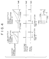
- FIG. 1 is a block diagram for illustrating schematic structure of an electronic still camera to which the present invention is applied.
- a camera of the present invention uses a CCD image sensing element 11 as a image sensing device, and is provided at least with a focus lens 12 for focusing an incident light emitted from an object (not shown in the drawing) on a light receiving plane of the CCD image sensing element, a component for shielding the incident light irradiated onto the CCD image sensing element 11 such as a mechanical shutter 13, and a timing pulse generation circuit 14 for generating various timing pulses to drive the CCD image sensing element 11.
- the camera is additionally provided with a recording device 15 for processing electrically output signals of the CCD image sensing element 11 and recording two image information items independently, and an image synthesis device 16 for synthetically processing two image information items recorded independently in the recording device 15, and structured so that one image information out of two image information items recorded independently in a memory medium 15 is sent out and a synthesized image information synthesized by the image synthesis device 16 is sent out.
- the recording device 15 and the image synthesis device 16 may not be combined to the camera.
- the mechanical shutter 13 is used as a light shielding means for shielding the incident light irradiated onto the light receiving plane of the CCD image sensing element, however other shielding means other than the mechanical shutter may be used without restriction, and alternatively, for example, a liquid crystal shutter may be used.
- the CCD image sensing element 11 is a so-called full pixel reading type CCD image sensing element, which reads out signal charges of all the pixels at a time to a vertical CCD register, and a CCD image sensing element 11 having the number of electric charge packets of a vertical CCD register equal to or more than the number of photoelectric conversion elements is used.
- the electric packet means a unit which treats a group of signal charges equivalent to one signal component.
- FIG. 2 One example of the structure of an interline transfer type CCD image sensing element is shown in FIG. 2.
- an image sensing unit 21 comprises a plurality of photodiodes 22, namely photoelectric conversion elements, arranged in the form of two-dimensional matrix, and a plurality of vertical CCD registers 24, which are provided for each vertical line of the photodiodes, served for vertical transfer of signal charge read from photodiodes 22 through gates 23.
- the vertical CCD register 24 of this example has the number of electric charge packets 25 approximately equivalent to the number of photodiodes 22 as shown in FIG. 2.
- a horizontal CCD register 26 is provided adjacent to and along the arrangement of the ends of the vertical CCD registers 24.
- the horizontal CCD register 26 transfers horizontally one line signal charge shifted from the plurality of vertical CCD registers 24 through line shift operation.
- an electric charge detection amplifier 27 having, for example, the floating diffusion amplifier structure for detecting signal electric charge transferred successively from the horizontal CCD registers 26 and converting it to signal voltage.
- the output voltage of the electric charge detection amplifier 27 is derived as a CCD output through an output terminal 28.
- the above-mentioned components are integrated on a semiconductor substrate (not shown in the drawing) in the form of an interline transfer type CCD image sensing element 20.
- the CCD image sensing element 20 having the structure described herein above performs various operations in response to various timing pulses such as electronic shutter pulse, read pulse, and vertical/horizontal transfer pulse supplied from the timing pulse generation circuit 14 shown in FIG. 1.
- Electronic shutter operation that signal charge accumulated in the photodiodes 22 is swept to the substrate is performed in response to the electronic shutter pulse given to the semiconductor substrate, electric read operation that signal charge accumulated in the photodiodes 22 is read to the vertical CCD registers 24 is performed in response to the read pulse given to the read gates 23, and vertical/horizontal transfer operation of signal charge is performed in response to the vertical/horizontal transfer pulse given to the vertical CCD registers 24/horizontal CCD register 26.
- the timing pulse generation circuit 14 for generating various timing pulses has a first driving means for determining the accumulation time of signal charge in the photodiodes 22 and second driving means for controlling the holding (accumulation) state of signal charge in the photodiodes 22.
- each photodiodes 22 accumulation of electric charge starts from the time point when the light receiving plane of a CCD image sensing element 20 starts to receive the incident light through the mechanical shutter 13 with unshielding operation (shutter operation) of the mechanical shutter 13 shown in FIG. 1 or from the time point when sweeping of signal charge from the photodiode 22 to the substrate with electronic shutter operation is completed, the accumulation of electric charge goes to an end at the time point when read of signal charge from the photodiode 22 to the vertical CCD register 24 in reading out operation is completed, and the next accumulation of electric charge starts from this time point.
- the CCD image sensing element 20 having the number of photodiodes 22 approximately equal to the number of electric charge packets 25 of the vertical CCD registers 24 is used, however the CCD image sensing element 20 is by no means limited to the case, a CCD image sensing element having the number of photodiodes 22 twice the number of electric charge packets 25 of the vertical CCD registers 24 may be used in the present invention as long as the CCD image sensing element is an interline transfer type CCD element by using 1/2 photodiodes 22 in 1 frame or 1 field or by employing the structure in which 2 pixels of signal charge of the photodiodes 22 are added.
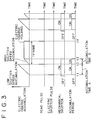
- the mechanical shutter 13 is open before the time t1, and later the signal charge which has been accumulated in the photodiode 22 is reset at the time t1 in response to an electronic shutter pulse.
- the signal charge is discharged (swept) from the photodiode 22 to the substrate by applying an electronic shutter pulse on the substrate. Accumulation of signal charge to the photodiode 22 starts from the time point when the reset operation ends.
- the photodiode 22 when the light signal starts to enter into the empty photodiode 22 through mechanical shutter 13, the signal charge is accumulated gradually with time in the photodiodes 22 due to photoelectric conversion effect.
- the read gate 23 opens, and the signal charge accumulated in the photodiode 22 is read to the vertical CCD register 24 through the read gate 23.
- the photodiode 22 becomes empty.
- the first accumulation time A is determined based on the time different between the time t2 and the time t1, the signal charge accumulated in the accumulation time A is accumulated in each electric packet 26 of the vertical CCD register 24.
- the signal charge read to the vertical CCD register 24 in the accumulation time A is discharged as a voltage signal in the time period from the time t2 to time t4 from the CCD image sensing element 20 through the electric charge detection amplifier 27 by way of vertical charge transfer by the vertical CCD register 24 and by way of horizontal charge transfer by the horizontal CCD register 26, and the electric charge packet 26 of the vertical CCD register 24 becomes empty.
- the photodiode 22 which has become empty at the time t2 starts to accumulate signal charge again because the mechanical shutter 13 is open. The accumulation is brought to an end at the time t3 when the mechanical shutter 13 is closed to shut out the light signal.
- the mechanical shutter13 In the time period from the time t3 to the time t4, the mechanical shutter13 is closed, and the signal charge accumulated in the accumulation time B is held in the photodiode 22.
- a read pulse is applied on the read gate 23 at the time t4, and the signal charge held in the photodiode 22 is read to the vertical CCD register 24 through the read gate 23.
- the signal charge accumulated in the accumulation time B and read to the vertical CCD register 24 is discharged as a voltage signal from the CCD image sensing element through the electric charge detection amplifier 27 by way of vertical electric charge transfer by the vertical CCD register 24 and by way of horizontal electric charge transfer by the horizontal CCD register 26 after the time t4.
- the signal charge accumulated in the electric charge packet 25 of the vertical CCD register 24, dark signal charge, and smear electric charge may be discharged by driving the vertical CCD register 24 just before the time t2.
- dark signal charge and smear electric charge accumulated in the packet of the vertical CCD register 24 may be discharged in the time period from the time point when the packet of the vertical CCD register 24 becomes empty just before the time t4 to the time point when the signal charge accumulated in the accumulation time B is read to the vertical CCD register 24.
- the structure in which the signal charge accumulated in the longer accumulation time is obtained prior to the signal charge accumulated in the shorter accumulation time is employed, but alternatively, the signal charge accumulated in the shorter accumulation time may be obtained prior to the signal charge accumulated in the longer accumulation time. Because the time period from the time t1 to the time t2 is all determined with electric timing by obtaining the signal charge accumulated in the shorter accumulation time as described herein above, this method is advantageous in that the accumulation time is obtained precisely. As the result, error of individual accumulation time is reduced.
- the accumulation is started at the time t1 by electronic shutter operation, but alternatively the accumulation is started by mechanical shutter operation (namely unshielding operation of the mechanical shutter 13) instead of electronic shutter operation.
- mechanical shutter operation namely unshielding operation of the mechanical shutter 13
- electronic shutter operation is advantageous in that accuracy of accumulation time setting is better.
- Two image information items are subjected to image signal processing in the recording device 15 and recorded independently in the recording medium.
- the independent recording of two image information items is advantageous in that usual signal processing is applied as it is, and two image information items are edited into desired image information at any time by image synthesis processing using a personal computer with aid of software.
- an electronic still camera which can be used with switching to usual image sensing and image sensing in accordance with the present invention is realized by combining the function of the present invention.
- two image information items recorded independently in the recording device 15 are synthesized by the image synthesis device 16 to form a one image information and the synthesized image information is sent out, and the image sensing result based on the function of the present invention is confirmed.
- simple processing can be applied because regular synthetic processing is performed later.
- the present invention by using the general solid-state image sensing element and the shielding means for shielding the incident light irradiated onto the light receiving plane of the image sensing element and by setting the driving timing of these components suitably, two image information items having different accumulation time with adjacent accumulation period are obtained without deterioration of vertical resolution.
Landscapes
- Engineering & Computer Science (AREA)
- Multimedia (AREA)
- Signal Processing (AREA)
- Transforming Light Signals Into Electric Signals (AREA)
- Solid State Image Pick-Up Elements (AREA)
Abstract
Description
Claims (14)
- An image sensing apparatus comprising:a plurality of photoelectric conversion elements;a solid-state image sensing element having an electric charge transfer unit for transferring signal charge read from these photoelectric conversion elements;light shielding means for shielding an incident light irradiated onto the light receiving plane of said solid-state image sensing element;first driving means having a function that the start of the first accumulation time in said photoelectric conversion elements is determined by electronic shutter operation of said solid-state image sensing element or unshielding operation of said light shielding means, the end of said first accumulation time and the start of the second accumulation time are determined by read operation of the signal charge from said photoelectric conversion elements to said electric charge transfer unit, and the end of the second accumulation time is determined by light shielding start operation of said light shielding means; andsecond driving means having a function that the second signal charge corresponding to said second accumulation time is accumulated and held in said photoelectric conversion elements until the first signal charge corresponding to said first accumulation time is transferred and the electric charge packet of said electric charge transfer unit becomes empty.
- An image sensing apparatus as claimed in claim 1, further comprising recording means for recording independently first image information based on said first signal charge and second image information based on said second signal charge.
- An image sensing apparatus as claimed in claim 2, further comprising image synthesis means for synthesizing the first and second image information items recorded by said recording means.
- An image sensing apparatus as claimed in claim 1, wherein said first accumulation time is shorter than said second accumulation time.
- An image sensing apparatus as claimed in claim 1, wherein the electric charge transfer unit is driven just before read operation of said first signal charge or said second signal charge to discharge unnecessary electric charge.
- An image sensing apparatus as claimed in claim 1, wherein the number of electric charge packets in said electric charge transfer unit of said solid-state image sensing element is almost the same as that of said plurality of photoelectric conversion elements.
- An image sensing apparatus as claimed in claim 1, wherein electric charge packets in said electric charge transfer unit of said solid-state image sensing element are fewer than said plurality of photoelectric conversion elements.
- An image sensing apparatus as claimed in claim 1, wherein said solid-state image sensing element is of interline type.
- A driving method of an image sensing apparatus comprising a plurality of photoelectric conversion elements, a solid-state image sensing element having an electric charge transfer unit for transferring signal charge read from these photoelectric conversion elements, and light shielding means for shielding the incident light irradiated onto the light receiving plane of said solid-state image sensing element,
wherein the start of the first accumulation time in said photoelectric conversion elements is determined by electronic shutter operation of said solid-state image sensing element or light unshielding operation of said light shielding means,the end of said first accumulation time and the start of the second accumulation time are determined by read operation of signal electric charge from said photoelectric conversion elements to said electric charge transfer unit,the end of said second accumulation time is determined by light shielding start operation of said light shielding means, andthe second signal charge corresponding to said second accumulation time is accumulated and held in said photoelectric conversion elements until the first signal charge corresponding to said first accumulation time is transferred and the electric charge packet of said electric charge transfer unit becomes empty. - A driving method of an image sensing apparatus as claimed in claim 9, wherein said first accumulation time is shorter than said second accumulation time.
- A driving method of an image sensing apparatus as claimed in claim 9, wherein the electric charge transfer unit is driven just before read operation of said first signal charge or said second signal charge to discharge unnecessary electric charge.
- A driving method of an image sensing apparatus as claimed in claim 9, wherein the number of electric charge packets in said electric charge transfer unit of said solid-state image sensing element is almost the same as that of said plurality of photoelectric conversion elements.
- A driving method of an image sensing apparatus as claimed in claim 9, wherein electric charge packets in said electric charge transfer unit of said solid-state image sensing element are fewer than said plurality of photoelectric conversion elements.
- A driving method of an image sensing apparatus as claimed in claim 9, wherein said solid-state image sensing element is of interline type.
Applications Claiming Priority (2)
| Application Number | Priority Date | Filing Date | Title |
|---|---|---|---|
| JP2936898 | 1998-02-12 | ||
| JP10029368A JPH11234572A (en) | 1998-02-12 | 1998-02-12 | Imaging device and driving method thereof |
Publications (2)
| Publication Number | Publication Date |
|---|---|
| EP0936809A2 true EP0936809A2 (en) | 1999-08-18 |
| EP0936809A3 EP0936809A3 (en) | 2000-08-23 |
Family
ID=12274225
Family Applications (1)
| Application Number | Title | Priority Date | Filing Date |
|---|---|---|---|
| EP99102100A Withdrawn EP0936809A3 (en) | 1998-02-12 | 1999-02-02 | Image sensing apparatus and driving method thereof |
Country Status (2)
| Country | Link |
|---|---|
| EP (1) | EP0936809A3 (en) |
| JP (1) | JPH11234572A (en) |
Cited By (2)
| Publication number | Priority date | Publication date | Assignee | Title |
|---|---|---|---|---|
| CN101459783B (en) * | 2007-12-13 | 2013-03-20 | 三星电子株式会社 | Digital photographing apparatus and method of operating image pickup device |
| US8587692B2 (en) | 2009-08-31 | 2013-11-19 | Samsung Electronics Co., Ltd | Method and apparatus for increasing dynamic range of image by using electronic shutter |
Families Citing this family (1)
| Publication number | Priority date | Publication date | Assignee | Title |
|---|---|---|---|---|
| JP2008092251A (en) * | 2006-10-02 | 2008-04-17 | Pentax Corp | Digital camera |
Family Cites Families (3)
| Publication number | Priority date | Publication date | Assignee | Title |
|---|---|---|---|---|
| US5638118A (en) * | 1987-06-09 | 1997-06-10 | Canon Kabushiki Kaisha | Image sensing device with diverse storage times used in picture composition |
| EP0387817A3 (en) * | 1989-03-16 | 1991-12-11 | Konica Corporation | Electronic still camera |
| JP3074967B2 (en) * | 1992-10-27 | 2000-08-07 | 松下電器産業株式会社 | High dynamic range imaging / synthesis method and high dynamic range imaging apparatus |
-
1998
- 1998-02-12 JP JP10029368A patent/JPH11234572A/en active Pending
-
1999
- 1999-02-02 EP EP99102100A patent/EP0936809A3/en not_active Withdrawn
Cited By (3)
| Publication number | Priority date | Publication date | Assignee | Title |
|---|---|---|---|---|
| CN101459783B (en) * | 2007-12-13 | 2013-03-20 | 三星电子株式会社 | Digital photographing apparatus and method of operating image pickup device |
| US8587692B2 (en) | 2009-08-31 | 2013-11-19 | Samsung Electronics Co., Ltd | Method and apparatus for increasing dynamic range of image by using electronic shutter |
| US8994849B2 (en) | 2009-08-31 | 2015-03-31 | Samsung Electronics Co., Ltd | Method and apparatus for increasing dynamic range of image by using electronic shutter |
Also Published As
| Publication number | Publication date |
|---|---|
| JPH11234572A (en) | 1999-08-27 |
| EP0936809A3 (en) | 2000-08-23 |
Similar Documents
| Publication | Publication Date | Title |
|---|---|---|
| US4881127A (en) | Still video camera with electronic shutter and flash | |
| JP2520581B2 (en) | Video camera | |
| JPH08223465A (en) | Electronic camera with fast automatic focusing of images on a progressive scan image sensor | |
| KR930018973A (en) | Solid state imaging device | |
| JPH0265380A (en) | Imaging device | |
| EP0936809A2 (en) | Image sensing apparatus and driving method thereof | |
| JPH02142183A (en) | Driving method of solid-state image sensor | |
| JPH0414554B2 (en) | ||
| JP2692219B2 (en) | Solid-state imaging device | |
| JPH04237271A (en) | Image pickup device | |
| JP3255464B2 (en) | Image sensor driving method and device | |
| JPH0965213A (en) | Image pickup device | |
| JP4174860B2 (en) | CCD imaging device | |
| JPS6367977A (en) | Image pickup device | |
| JP2647547B2 (en) | Imaging device and solid-state imaging device driving device | |
| JP3340482B2 (en) | Method and apparatus for sweeping out unnecessary charge of image sensor | |
| JP2647549B2 (en) | Imaging device and solid-state imaging device driving device | |
| JP2549653B2 (en) | Solid-state image sensor camera | |
| JPH04225687A (en) | Image pickup device | |
| JPH04257171A (en) | Imaging device | |
| JP2003078819A (en) | Solid-state imaging device and charge sweeping method thereof | |
| JPH04167776A (en) | Imaging device and solid-state imaging device drive device | |
| JPH0654245A (en) | Driving system for solid state image pickup element | |
| JPH0297179A (en) | Solid image pickup element, solid image pickup element driving device and image pickup device | |
| JPH0477512B2 (en) |
Legal Events
| Date | Code | Title | Description |
|---|---|---|---|
| PUAI | Public reference made under article 153(3) epc to a published international application that has entered the european phase |
Free format text: ORIGINAL CODE: 0009012 |
|
| AK | Designated contracting states |
Kind code of ref document: A2 Designated state(s): DE FR GB |
|
| AX | Request for extension of the european patent |
Free format text: AL;LT;LV;MK;RO;SI |
|
| PUAL | Search report despatched |
Free format text: ORIGINAL CODE: 0009013 |
|
| AK | Designated contracting states |
Kind code of ref document: A3 Designated state(s): AT BE CH CY DE DK ES FI FR GB GR IE IT LI LU MC NL PT SE |
|
| AX | Request for extension of the european patent |
Free format text: AL;LT;LV;MK;RO;SI |
|
| RIC1 | Information provided on ipc code assigned before grant |
Free format text: 7H 04N 5/335 A, 7H 04N 5/235 B, 7H 04N 3/15 B, 7H 04N 5/33 B |
|
| 17P | Request for examination filed |
Effective date: 20010123 |
|
| 17Q | First examination report despatched |
Effective date: 20010323 |
|
| AKX | Designation fees paid |
Free format text: DE FR GB |
|
| GRAH | Despatch of communication of intention to grant a patent |
Free format text: ORIGINAL CODE: EPIDOS IGRA |
|
| STAA | Information on the status of an ep patent application or granted ep patent |
Free format text: STATUS: THE APPLICATION IS DEEMED TO BE WITHDRAWN |
|
| 18D | Application deemed to be withdrawn |
Effective date: 20030520 |