EP0936764B1 - Verfahren und Einrichtung zur Kalibrierung von digitalen Frequenzumsetzern in einem Signalverarbeitungssystem - Google Patents
Verfahren und Einrichtung zur Kalibrierung von digitalen Frequenzumsetzern in einem Signalverarbeitungssystem Download PDFInfo
- Publication number
- EP0936764B1 EP0936764B1 EP99300976A EP99300976A EP0936764B1 EP 0936764 B1 EP0936764 B1 EP 0936764B1 EP 99300976 A EP99300976 A EP 99300976A EP 99300976 A EP99300976 A EP 99300976A EP 0936764 B1 EP0936764 B1 EP 0936764B1
- Authority
- EP
- European Patent Office
- Prior art keywords
- phase
- digital down
- down converter
- peak
- quadrature
- Prior art date
- Legal status (The legal status is an assumption and is not a legal conclusion. Google has not performed a legal analysis and makes no representation as to the accuracy of the status listed.)
- Expired - Lifetime
Links
Images


Classifications
-
- G—PHYSICS
- G01—MEASURING; TESTING
- G01B—MEASURING LENGTH, THICKNESS OR SIMILAR LINEAR DIMENSIONS; MEASURING ANGLES; MEASURING AREAS; MEASURING IRREGULARITIES OF SURFACES OR CONTOURS
- G01B21/00—Measuring arrangements or details thereof, where the measuring technique is not covered by the other groups of this subclass, unspecified or not relevant
-
- G—PHYSICS
- G01—MEASURING; TESTING
- G01S—RADIO DIRECTION-FINDING; RADIO NAVIGATION; DETERMINING DISTANCE OR VELOCITY BY USE OF RADIO WAVES; LOCATING OR PRESENCE-DETECTING BY USE OF THE REFLECTION OR RERADIATION OF RADIO WAVES; ANALOGOUS ARRANGEMENTS USING OTHER WAVES
- G01S3/00—Direction-finders for determining the direction from which infrasonic, sonic, ultrasonic or electromagnetic waves, or particle emission, not having a directional significance, are being received
- G01S3/80—Direction-finders for determining the direction from which infrasonic, sonic, ultrasonic or electromagnetic waves, or particle emission, not having a directional significance, are being received using ultrasonic, sonic or infrasonic waves
- G01S3/82—Direction-finders for determining the direction from which infrasonic, sonic, ultrasonic or electromagnetic waves, or particle emission, not having a directional significance, are being received using ultrasonic, sonic or infrasonic waves with means for adjusting phase or compensating for time-lag errors
-
- H—ELECTRICITY
- H04—ELECTRIC COMMUNICATION TECHNIQUE
- H04L—TRANSMISSION OF DIGITAL INFORMATION, e.g. TELEGRAPHIC COMMUNICATION
- H04L27/00—Modulated-carrier systems
- H04L27/0014—Carrier regulation
-
- H—ELECTRICITY
- H04—ELECTRIC COMMUNICATION TECHNIQUE
- H04L—TRANSMISSION OF DIGITAL INFORMATION, e.g. TELEGRAPHIC COMMUNICATION
- H04L27/00—Modulated-carrier systems
- H04L27/0014—Carrier regulation
- H04L2027/0024—Carrier regulation at the receiver end
Definitions
- the present invention relates generally to the field of signal processing, and more specifically to a method and apparatus for calibration of digital down converters in a signal processing system.
- Acoustic listening systems for underwater applications are well known in the art.
- modem military submarines are equipped with arrays of acoustic sensors which provide sensitive underwater listening capabilities and even relative position information.
- Each sensor reacts to an incoming pressure wave by modulating an input signal and the outputs of all the sensors are processed to determine the sound and position information.
- These sensor arrays are generally either attached to the submarine hull or are towed behind the submarine. Ideally, the sensors would be attached to the submarine hull, but prior art acoustic sensors were simply too heavy for many submarine applications.
- Recent advances in acoustic sensor array technology however, have produced arrays which are light enough to be mounted on a submarine hull and which still provide very sensitive signal response. This weight reduction has also allowed the number of sensors to be increased.
- Vast arrays of sensors may be placed on the ocean bottom in the vicinity of known oil reserves.
- a surface ship then initiates an acoustic pressure wave (i.e. a large air burst).
- the acoustic pressure wave and its reflection off the ocean floor are detected by the sensor arrays.
- the data from the sensors is then processed and analyzed to determine optimum drilling locations or to monitor the status of known reservoirs.
- a calibration technique for digital down converters in a signal processing system wherein a digital down converter is selected by a system controller for calibration.
- the digital down converter's settings are copied into a calibration digital down converter which mimics the operation of the selected digital down converter.
- a best polarization diversity detector signal path, an optimal phase offset value for an in-phase data signal, an optimal phase offset value for a quadrature phase data signal, and a normalized gain value for the in-phase and quadrature phase signals of the selected digital down converter are determined.
- the system controller updates the selected digital down converter with the determined optimal settings. This procedure is repeated for each digital down converter in the signal processing system, while the signal processing occurs simultaneously.
- the process of selecting the best polarization diversity detector signal path further comprises the steps of selecting a first signal path, obtaining in-phase or quadrature phase data samples, determining a maximum in-phase or quadrature phase peak-to-peak value, saving the determined maximum in-phase or quadrature phase peak-to-peak value, repeating the above steps for each signal path, comparing the saved maximum in-phase or quadrature phase peak-to-peak values, and selecting a signal path with a largest peak-to-peak value as the best polarization diversity detector signal path.
- the process of determining an optimal in-phase offset value comprises the steps of writing a phase offset to the calibration digital down converter, obtaining in-phase and quadrature phase data samples, calculating a peak-to-peak value when the quadrature signal is near zero, comparing the calculated peak-to-peak value with a previously determined peak-to-peak value, saving whichever peak-to-peak value is larger, and repeating the above steps for each possible phase offset.
- the process of normalizing a gain value for the in-phase and quadrature phase signals of the selected digital down converter comprises the steps of reading an in-phase and a quadrature phase gain setting, obtaining in-phase and quadrature phase data samples, comparing the in-phase and quadrature phase data samples, calculating a new in-phase gain, when the in-phase data is larger than the quadrature phase peak-to-peak value, by multiplying the in-phase gain setting by the quotient [Q/I], and calculating a new quadrature phase gain, when the quadrature phase peak-to-peak value is larger than the in-phase peak-to-peak value, by multiplying the quadrature phase gain setting by the quotient [I/Q].
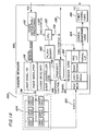
- Figure 1(A) is a high-level block diagram of a submarine system 100 incorporating the present invention.
- An inboard receiver module 102 contains the requisite electronic control and processing circuitry and is located inside the submarine.
- a light weight array of fiber optic interferometric sensors 104 is located on the hull (i.e operates in the water) of the submarine. Each sensor reacts to an incoming acoustic pressure wave by modulating a light signal 118 sent from the inboard receiver 102. Modulated signals from different sensors (each operating at a different carrier frequency) are passively multiplexed onto a single fiber optic cable and sent back to the receiver. The channel signals are then demultiplexed and demodulated by the receiver 102.
- the inboard receiver 102 is connected to the submarine's power system via a power connection 106.
- the inboard receiver 102 has a power distribution and conditioning block 112 to provide the necessary power requirements for the receiver components.
- the input light signal 118 is generated by a laser module 116.
- the laser module includes a laser, a phase modulator, a laser driver card and a laser controller card.
- the laser used in the preferred embodiment is a Model 125 200 mW Nd:YAG laser available from Lightwave Electronics of Palo Alto, California.
- the preferred embodiment uses eight lasers 117a - 117h which drive eight corresponding sensor arrays 104a - 104h.
- Each laser powers 56 sensors (channels), 28 channels on each side of the submarine.
- Each laser is modulated by a phase modulator 119a - 119h injecting a sine wave signal.
- Each phase modulator 119a - 119h injects a different frequency sine wave [1.5 MHz to 2.2 MHz in the preferred embodiment].
- Each laser's wavelength is nominally at 1319 nanometers, but each laser operates at a different "color" around 1319 nanometers.
- the frequency synthesizer 142 controls the temperature of each laser separately, as is well known in the art, in order to produce eight different "colors.”
- the first channels from each sensor array are multiplexed via a signal multiplexor 121. This a total of 56 fiber optic cables return from the sensor array 104, with each fiber carrying eight multiplexed signals.
- This multiplexed signal is then processed by a receiver card 122. Depending upon the number of sensors used, several receiver cards may be needed.
- the frequency synthesizer 142 contains the master system clock and controls the operation of the laser module, specifically, such parameters as laser color, power, temperature monitoring, etc. Timing information is provided to the receiver card via a signal line 144.
- a CPU 130 and associated memory 140 provide system level control and status information to the other receiver 102 components via data lines 132, 134, 138.
- the CPU 130 also controls a "gross" calibration procedure for the laser modules, a detailed description of which is beyond the scope of the present invention.
- the receiver card 122 demultiplexes and demodulates the return signal 120 and outputs a signal to a common beamformer card 124 which provides additional signal processing.
- a fiber channel card 126 provides the signal information to an external fiber bus 110. In the preferred embodiment, each receiver card 122 processes the signals from 7 return fibers, or a total of 56 channels.
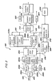
- FIG. 2 is a detailed block diagram of the receiver card 122 shown in Figure 1.
- the signal ⁇ ( ⁇ (t)) 120 (containing 8 channels) output by the acoustic sensor array is input to a polarization diversity detector (PDD) 200.
- PDD polarization diversity detector
- An example of a PDD which has three outputs is described in U.S Patent No. 5,448,058, entitled "OPTICAL SIGNAL DETECTION APPARATUS AND METHOD FOR PREVENTING POLARIZATION SIGNAL FADING IN OPTICAL FIBER INTERFEROMETRIC SENSOR SYSTEMS.”
- a bi-cell or two output PDD is used.
- the PDD 200 prevents polarization signal fading in the return signal 120.
- the PDD 200 converts the photonic energy of the return optical fiber signal 120 into two separate electrical currents 200a, 200b via two photodiodes (not shown).
- a transimpedance amplifier converts the input current to a voltage.
- a variable gain amplifier sets the voltage level to maximize the signal-to-noise level and to ensure that the voltage level is below the saturation level of the ADCs 204a, 204b.
- Anti-aliasing filters in the opto-receivers 202a, 202b filter the signal which then passes to the ADCs 204a, 204b.
- a digital-to-analog converter (DAC) 234 creates a gain value from a digital gain value output by the system controller 226 for each variable gain amplifier in each opto-receiver 202a, 202b.
- DAC digital-to-analog converter
- the analog outputs of the opto-receivers 202a, 202b are then digitized by high speed (>25.6 MSPS), high resolution (> 12-bit) analog-to-digital converters (ADCs) 204a, 204b.
- the ADC used in the preferred embodiment is part number 9042, manufactured by Analog Devices, Inc.
- the number of ADCs used is directly dependent upon the number of outputs from the PDD 200. Typically, there are two outputs, but three is possible.
- the digitized output contains a complex signal comprised of all channels of the frequency division multiplexed phase generated carriers with their information carrying sidebands on the return optical fiber signal 120.
- Each ADC 204a, 204b output is buffered and passed through to a multi-throw, multi-pole bus switch 206 which taps into each ADC 204a, 204b signal path.
- One output of the bus switch 206 goes to a digital down converter (DDC) 228, via signal path 238, which is employed as part of a calibration channel, as described below.
- DDC digital down converter
- the outputs of the bus switch 206 go to the signal channel DDCs 208a, 208b, 208n.
- the purpose of the bus switch 206 is to allow each of the DDCs to be able to connect to any ADC output. This is required by the PDD selection algorithm, discussed below with reference to Figure 6.
- Each DDC 208a, 208b, 208n acts as a digital demultiplexer by performing mix down and filtering of the digital information, separating one channel out of the composite signal.
- the DDC chip employed in the presently preferred embodiment is the GC4014 chip manufactured by Graychip, Inc. This particular device has 2 channel capability. In other embodiments, each chip may only have 1/2 channel capability.
- the number of DDCs needed depends upon the number of channels used in a given application. For example, if the input signal 120 has 8 multiplexed channels, then 4 DDC chips are needed. In the present embodiment, 28 DDCs (56 channels) are used per receiver card 122, but only one calibration DDC and system controller are required (as described below). Thus, seven channel groups are needed to process all 56 multiplexed signals (8 channels per multiplexed array output signal).
- Each DDC 208a, 208b, 208n outputs both in-phase (I) and quadrature phase (Q) words that represent the rectangular components of the phase.
- I and Q components from the DDCs 208a, 208b, 208n are time division multiplexed (TDM) onto separate I and Q buses.
- the output signal paths 210, 212 (which are serial, unidirectional data paths in the preferred embodiment) output the I and Q 8-bit words to a buffer 214 which buffers the words and also converts the 8 bit words into 16 bit words.
- the I and Q words are demodulated from all of the DDCs in a time sequence.
- the I and Q words are converted from Cartesian to polar form by the coordinate transformer 216.
- the coordinate transformer 216 of the preferred embodiment is a TMC2330A chip manufactured by Raytheon Corp., but may be any similar device.
- the output of the coordinate transformer 216 is the instantaneous phase angle, whose change is directly related to the change in acoustic pressure of the acoustic signal from the environment and whose rate of change is directly related to the frequency of the acoustic signal from the environment for a given fiber optic sensor.
- the channel-by-channel instantaneous phase angles are further processed in an acoustic signal processor 218 with integration and filtering algorithms.
- the output of the acoustic signal processor 218 may then be provided to a visual display or further signal processing blocks, as desired.
- Two DACs 222, 224 provide I and Q signals which can be used for testing or viewing the output signal.
- the I and Q signals may be connected to the X and Y inputs of an oscilloscope in order to view a graphical representation of the I and Q signals.
- the output 238 of the bus switch 206 feeds the calibration channel DDC 228. If there is more than one PDD 200, there will be more than one bus switch 206 feeding the calibration channel DDC 228 in a TDM manner.
- the calibration channel DDC 228 is set to mimic each signal channel in turn.
- the calibration channel provides a way to check PDD output selection, phase shift adjustment and I/Q balance on a per signal channel basis in a non-obtrusive way.
- the data is processed by the DDC 228 into I and Q words similar to the signal channel DDCs 208a, 208b, 208n.
- the I and Q words are processed by the system controller 226 to extract the information necessary to determine channel performance.
- the system controller 226 of the preferred embodiment is a ADSP 2181 manufactured by Analog Devices, Inc.
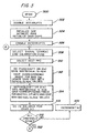
- a phase shift algorithm for the Q component is performed at step 314, as shown in Figure 5.
- An I/Q balance algorithm is executed at step 316, which is shown in detail in Figure 7. Steps 308 - 316 are repeated for each channel, until all the channels have been calibrated. In one embodiment, calibration is performed only at system start-up. In the preferred embodiment, however, the calibration procedure continues for each DDC for as long as the system is operating. This results in a dynamic calibration system which unobtrusively calibrates the system, while signal processing functions are unaffected.
- step 310) The procedure for selecting the best PDD signal (step 310) is illustrated by the flowchart of Figure 6.
- the first ADC 204a is selected, and I and Q data samples are obtained at step 604.
- a maximum I peak-to-peak value is calculated at step 606.
- the maximum I peak-to-peak value determined at step 606 is then stored at step 608.
- the second ADC 204b is selected at step 610.
- I and Q data samples are then obtained for the second ADC 204b at step 612.
- a maximum I peak-to-peak value is calculated at step 614, and this value is stored at step 616.
- the two stored maximum I peak-to-peak values are then compared at step 618.
- the ADC which produces the larger I peak-to-peak value is then selected (steps 620, 622). Since selecting different ADCs will affect the I and Q signal levels symmetrically, only one signal (I or Q) needs to be examined. Note that the PDD selection step is performed for each channel separately. Thus, different DDC may actually be using different ADC inputs, which is why each DDC needs to be connected to both ADCs.
- phase shift algorithm for the I component (step 312) and the Q component (step 314) are shown in Figures 4 and 5, respectively.
- the purpose of this algorithm is to determine the phase offsets that result in a maximum phase signal (I data) and quadrature phase signal (Q data) for each channel. This is accomplished by programming the calibration DDC's 228 channel control registers with different phase offsets having equal phase increments and reading the corresponding I and Q data from the channel output registers.
- the I and Q data generated by the calibration DDC 228 will be read by the system controller 226 and stored into two separate buffers. Once a sufficient number of data samples have accumulated, the phase shift algorithm will be performed on the I and Q data.
- the output of the phase shift algorithms will generate an I-phase offset and a Q-phase offset, which are the offsets that result in maximum amplitude I and Q signals. These optimal offset values will then be stored in the associated signal channel DDC.
- a phase increment is stored in the calibration DDC 228, and the I and Q data values are obtained.
- a maximum peak-to-peak value for I is calculated. In the present embodiment 32 samples are used, but depending upon the application, either more or less samples may be used. If the I value calculated at step 406 is greater to or equal to a previous value, then a MAX I(n) peak-to-peak variable is set equal to the current I value, and the corresponding phase is also saved at step 410. Otherwise, at step 412, the MAX I(n) variable is set equal to the previous value of I, and the corresponding phase value is saved. This procedure is repeated at step 402 until all I phase increments have been tested. The resulting MAX I(n) value is then stored into the corresponding DDC chip associated with the current channel.
- FIG. 7 is a flowchart illustrating the I/Q balance algorithm (step 316 of Figure 1). This procedure is necessary in order to normalize the maximum I and Q vectors in order to minimize the errors in angle calculations.
- the current I and Q gain settings for the current signal channel are read and the I and Q data samples are obtained for the current channel.
- the I and Q values are compared. If I is greater than Q, then a new I gain is calculated at step 706. The new I gain value is equal to the current I gain value multiplied by the quotient [Q/I]. If, however, I is not greater than Q, then a new Q gain value is calculated at step 708. The new Q gain value is equal to the current Q gain value multiplied by the quotient [I/Q]. The gain values are then re-written to the DDC of the current signal channel.
- control signal bus and the data bus for the DDCs are separate.
- the control signal path between the DDCs and the system controller is a separate bi-directional parallel bus.
- the data signals are output onto a separate serial bus.
- the background calibration operations are processed in parallel to the high speed signal data process flow.
- both high speed signal processing and background calibration processing can occur at the same time.
- both signal and control information share the same parallel bus, and, due to throughput limitations on the bus, the calibration routines are run only during startup or when there is a break in normal system operations.
Landscapes
- Engineering & Computer Science (AREA)
- Physics & Mathematics (AREA)
- General Physics & Mathematics (AREA)
- Computer Networks & Wireless Communication (AREA)
- Signal Processing (AREA)
- Radar, Positioning & Navigation (AREA)
- Remote Sensing (AREA)
- Optical Communication System (AREA)
- Analogue/Digital Conversion (AREA)
- Measurement Of Velocity Or Position Using Acoustic Or Ultrasonic Waves (AREA)
- Radio Transmission System (AREA)
Claims (9)
- Kalibrierungsverfahren für digitale Frequenzumwandler in einem Signalverarbeitungssystem, das folgende Schritte aufweist:Auswählen eines zu kalibrierenden Digitalfrequenzumwandlers (226) ;Kopieren der Einstellungen des ausgewählten Digitalfrequenzumwandlers in einen Kalibrierungs-Digitalfrequenzumwandler (228);Auswählen eines günstigsten Polarisationsdiversitätsdetektor-Signalpfades für den ausgewählten Digitalfrequenzumwandler (206);Berechnen eines optimalen Phasen-Offset-Wertes für ein In-Phase-Datensignal des ausgewählten Digitalfrequenzumwandlers (312) ;Berechnen eines optimalen Phasen-Offset-Wertes für ein Quadraturphasen-Datensignal des ausgewählten Digitalfrequenzumwandlers (314);Normalisieren eines Verstärkungswertes für die In-Phase-und Quadraturphasen-Signale des ausgewählten Digitalfrequenzumwandlers (316);Aktualisieren des ausgewählten Digitalfrequenzumwandlers mit einem bestimmten günstigsten Signalpfad, einem optimalen In-Phase-Offset-Wert, einem optimalen Quadraturphasen-Offset-Wert und einem normalisierten Verstärkungswert (226); undWiederholen der obigen Schritte für jeden Digitalfrequenzumwandler in dem Signalverarbeitungssystem während gleichzeitig die Signalverarbeitung stattfindet (308, 318).
- Verfahren nach Anspruch 1, bei dem die Schritte für jeden Digitalfrequenzumwandler beim Systemstart nur einmal durchgeführt werden.
- Verfahren nach Anspruch 1, bei dem die Schritte für jeden Digitalfrequenzumwandler so lange wiederholt werden, wie das Signalverarbeitungssystem in Betrieb ist.
- Verfahren gemäß einem der Ansprüche 1-3, bei dem der Schritt Auswählen des günstigsten Polarisierungsdiversitätsdetektor-Signalpfades weiterhin die Schritte umfaßt:Auswählen eines ersten Signalpfades;Erhalten von In-Phase- oder Quadraturphasen-Datensätzen;Bestimmen eines maximalen In-Phase- oder Quadraturphasen-Spitze-Spitze-Wertes;Abspeichern des ermittelten maximalen In-Phase- oder Quadraturphasen-Spitze-Spitze-Wertes;Wiederholen der obigen Schritte für jeden Signalpfad;Vergleichen der gespeicherten maximalen In-Phase- oder Quadraturphasen-Spitze-Spitze-Werte undAuswählen eines Signalpfades mit einem größten Spitze-Spitze-Wert als den günstigsten Polarisierungsdiversitätsdetektor-Signalpfad.
- Verfahren gemäß einem der Ansprüche 1-4, bei dem der Schritt Bestimmen eines optimalen In-Phase-Offset-Wertes folgende Schritte umfaßt:Schreiben eines Phasen-Inkrements in den Kalibrierungs-Digitalfrequenzumwandler;Erhalten von In-Phase- und Quadraturphasen-Datensätzen;Berechnen eines Spitze-Spitze-Wertes wenn das Quadratursignal nahe Null liegt;Vergleichen des berechneten Spitze-Spitze-Wertes mit einem vorher bestimmten Spitze-Spitze-Wert;Abspeichern des größten Spitze-Spitze-Wertes; undWiederholen der obigen Schritte für jedes mögliche Phasen-Inkrement.
- Verfahren gemäß einem der Ansprüche 1-5, bei dem der Schritt Bestimmen eines optimalen Quadratur-Offset-Wertes folgende Schritte aufweist:Schreiben eines Phasen-Inkrements in den Kalibrierungs-Digitalfrequenzumwandler;Erhalten von In-Phase- und Quadraturphasen-Datensätzen;Berechnen eines Spitze-Spitze-Wertes wenn das In-Phase-Signal nahe Null liegt;Vergleichen des berechneten Spitze-Spitze-Wertes mit einem vorher bestimmten Spitze-Spitze-Wert;Abspeichern des größten Spitze-Spitze-Wertes; undWiederholen der obigen Schritte für jedes mögliche Phasen-Inkrement.
- Verfahren nach einem der Ansprüche 1-6, bei dem der Schritt Normalisieren eines Verstärkungswertes für die In-Phase- und Quadraturphasen-Signale des ausgewählten Digitalfrequenzumwandlers folgende Schritte aufweist:Lesen einer In-Phase- und einer Quadraturphasen-Verstärkungseinstellung;Erhalten von In-Phase- und Quadraturphasen-Datensätzen;Vergleichen der In-Phase- und Quadraturphasen-Datensätze;Berechnen einer neuen In-Phase-Verstärkung, wenn die In-Phase-Daten größer sind als die Quadraturphasen-Daten, durch Multiplikation der In-Phase-Verstärkungseinstellung mit dem Quotienten [Q/I]; undBerechnen einer neuen Quadraturphasen-Verstärkung, wenn die Quadraturphasen-Daten größer sind als die In-Phase-Daten, durch Multiplikation der Quadraturphasen- Signalpfad erstärkungseinstellung mit dem Quotienten [I/Q].
- Vorrichtung zur Kalibrierung eines Digitalfrequenzumwandlers in einem Signalverarbeitungssystem, wobei die Vorrichtung aufweist:einen Kalibrierungs-Digitalfrequenzumwandler, der verbunden ist, um In-Phasen- und Quadratur-Phasen-Daten für einen ausgewählten Digitalfrequenzumwandler zu empfangen (228);einen Systemcontroller, der mit dem Digitalfrequenzumwandler und dem Kalibrierungs-Digitalfrequenzumwandler verbunden ist, wobei der Kalibrierungs-Digitalfrequenzumwandler, gesteuert durch den Systemcontroller, die Funktionsweise des Digitalfrequenzumwandlers nachahmt, um optimale Digitalfrequenzumwandler-Einstellungen zu bestimmen, und wobei der Systemcontroller die ermittelten optimalen Digitalfrequenzumwandler-Einstellungen aktualisiert, so daß der Digitalfrequenzumwandler gemäß der optimalen Einstellungen kalibriert ist (226).
- Vorrichtung nach Anspruch 8, bei der die zu ermittelnden optimalen Einstellungen einen günstigsten Polarisationsdiversitätsdetektor-Pfad, einen günstigsten In-Phase-Phasen-Offset-Wert, einen günstigsten Quadraturphasen-Offset-Wert, sowie einen normalisierten In-Phase- und Quadraturphasen-Verstärkungswert umfassen.
Applications Claiming Priority (2)
| Application Number | Priority Date | Filing Date | Title |
|---|---|---|---|
| US09/021,557 US6134281A (en) | 1998-02-10 | 1998-02-10 | Method and apparatus for calibration of a signal processing system utilizing digital down converters |
| US21557 | 1998-02-10 |
Publications (3)
| Publication Number | Publication Date |
|---|---|
| EP0936764A2 EP0936764A2 (de) | 1999-08-18 |
| EP0936764A3 EP0936764A3 (de) | 2001-05-23 |
| EP0936764B1 true EP0936764B1 (de) | 2006-07-12 |
Family
ID=21804891
Family Applications (1)
| Application Number | Title | Priority Date | Filing Date |
|---|---|---|---|
| EP99300976A Expired - Lifetime EP0936764B1 (de) | 1998-02-10 | 1999-02-10 | Verfahren und Einrichtung zur Kalibrierung von digitalen Frequenzumsetzern in einem Signalverarbeitungssystem |
Country Status (9)
| Country | Link |
|---|---|
| US (1) | US6134281A (de) |
| EP (1) | EP0936764B1 (de) |
| JP (1) | JP4287529B2 (de) |
| KR (1) | KR19990072552A (de) |
| AU (1) | AU746552B2 (de) |
| CA (1) | CA2259671A1 (de) |
| DE (1) | DE69932271T2 (de) |
| IL (1) | IL128452A (de) |
| NO (1) | NO990610L (de) |
Families Citing this family (15)
| Publication number | Priority date | Publication date | Assignee | Title |
|---|---|---|---|---|
| US6744826B2 (en) * | 1999-03-03 | 2004-06-01 | Intel Corporation | AGC window detector |
| US6314811B1 (en) * | 2000-01-24 | 2001-11-13 | Litton Systems Inc. | Acoustic sensor module design and fabrication process |
| DE60128099T2 (de) * | 2000-07-24 | 2008-01-03 | Litton Systems, Inc., Woodland Hills | Algorithmus zur auswahl einer detektionsmaske mit polarisationsdiversität |
| CA2420169A1 (en) * | 2000-07-28 | 2003-02-27 | William Christopher Knaack | Multi-channel optical receiver for processing tri-cell polarization diversity detector outputs |
| US20030165203A1 (en) * | 2001-08-10 | 2003-09-04 | Rishi Mohindra | Quadrature gain and phase imbalance correction in a receiver |
| US7346313B2 (en) | 2002-03-04 | 2008-03-18 | Cafarella John H | Calibration of I-Q balance in transceivers |
| KR100554922B1 (ko) * | 2002-10-18 | 2006-03-10 | 엘지전자 주식회사 | 다중 빔 기반의 다중경로 탐색장치 및 방법 |
| US7012245B2 (en) * | 2003-07-09 | 2006-03-14 | Northrop Grumman Corporation | Calculation of sensor array induced phase angle |
| US7038785B2 (en) * | 2003-07-09 | 2006-05-02 | Northrop Grumman Corporation | Filtered calculation of sensor array induced phase angle independent from demodulation phase offset of phase generated carrier |
| US8387037B2 (en) * | 2005-01-28 | 2013-02-26 | Ca, Inc. | Updating software images associated with a distributed computing system |
| AU2010313155A1 (en) * | 2009-11-02 | 2012-05-17 | Invention Plant, Llc | Detector system |
| US8089394B2 (en) | 2009-11-02 | 2012-01-03 | Invention Planet, LLC | Continuous-wave field disturbance sensing system |
| US8085185B2 (en) | 2009-11-02 | 2011-12-27 | Invention Planet, LLC | Method of down converting high-frequency signals |
| US8223067B2 (en) * | 2009-11-02 | 2012-07-17 | Invention Planet, LLC | Noise-canceling down-converting detector |
| CN110514355B (zh) * | 2019-02-12 | 2021-04-09 | 石家庄铁道大学 | 一种航空飞行器滑油室压力传感器校准装置及其校准方法 |
Family Cites Families (6)
| Publication number | Priority date | Publication date | Assignee | Title |
|---|---|---|---|---|
| US5493581A (en) * | 1992-08-14 | 1996-02-20 | Harris Corporation | Digital down converter and method |
| US5448058A (en) * | 1993-04-27 | 1995-09-05 | Litton Systems, Inc. | Optical signal detection apparatus and method for preventing polarization signal fading in optical fiber interferometric sensor systems |
| US5659412A (en) * | 1994-12-06 | 1997-08-19 | Lucent Technologies Inc. | Polarization diversity detection of optical signals transmitted through a polarization-mode dispersive medium |
| US5881376A (en) * | 1995-12-15 | 1999-03-09 | Telefonaktiebolaget Lm Ericsson | Digital calibration of a transceiver |
| US5982819A (en) * | 1996-09-23 | 1999-11-09 | Motorola, Inc. | Modulation format adaptive messaging receiver and method thereof |
| US5959294A (en) * | 1998-02-10 | 1999-09-28 | Litton Systems, Inc. | Method and apparatus for interrogation of fiber optic interferometric sensors in multi-channel applications |
-
1998
- 1998-02-10 US US09/021,557 patent/US6134281A/en not_active Expired - Lifetime
-
1999
- 1999-02-09 CA CA002259671A patent/CA2259671A1/en not_active Abandoned
- 1999-02-09 IL IL12845299A patent/IL128452A/xx not_active IP Right Cessation
- 1999-02-09 NO NO19990610A patent/NO990610L/no not_active Application Discontinuation
- 1999-02-09 AU AU16365/99A patent/AU746552B2/en not_active Expired
- 1999-02-10 DE DE69932271T patent/DE69932271T2/de not_active Expired - Fee Related
- 1999-02-10 KR KR1019990004624A patent/KR19990072552A/ko not_active Ceased
- 1999-02-10 JP JP03347999A patent/JP4287529B2/ja not_active Expired - Lifetime
- 1999-02-10 EP EP99300976A patent/EP0936764B1/de not_active Expired - Lifetime
Also Published As
| Publication number | Publication date |
|---|---|
| NO990610D0 (no) | 1999-02-09 |
| KR19990072552A (ko) | 1999-09-27 |
| JP2000028702A (ja) | 2000-01-28 |
| AU1636599A (en) | 1999-08-26 |
| IL128452A (en) | 2003-01-12 |
| DE69932271T2 (de) | 2006-11-30 |
| CA2259671A1 (en) | 1999-08-10 |
| IL128452A0 (en) | 2000-01-31 |
| EP0936764A3 (de) | 2001-05-23 |
| JP4287529B2 (ja) | 2009-07-01 |
| DE69932271D1 (de) | 2006-08-24 |
| NO990610L (no) | 1999-08-11 |
| US6134281A (en) | 2000-10-17 |
| AU746552B2 (en) | 2002-05-02 |
| EP0936764A2 (de) | 1999-08-18 |
Similar Documents
| Publication | Publication Date | Title |
|---|---|---|
| EP0936453B1 (de) | Verfahren und Anordnung zur Abfrage von faseroptischen interferometrischen Fühlern in Vielkanalanwendungen | |
| EP0936764B1 (de) | Verfahren und Einrichtung zur Kalibrierung von digitalen Frequenzumsetzern in einem Signalverarbeitungssystem | |
| AU740040B2 (en) | Method and apparatus for calibration of a multi-channel fiber optic interferometric sensor system in a signal processing system | |
| US6859419B1 (en) | Laser-based acousto-optic uplink communications technique | |
| EP1946053B1 (de) | Verfahren und system zum verwenden ungerader oberschwingungen für ein phasengeneriertes trägermoduliertes optisches signal | |
| JPS6352087A (ja) | 地震デ−タ収集装置の初期設定方法および装置 | |
| JP2002323383A (ja) | 強度ノイズを低減するための機能を有するヘテロダイン光スペクトル分析器 | |
| KR100491451B1 (ko) | 위상 생성 반송파 복조 및 직교 에러 정정을 하는 다중채널 간섭계 | |
| US6600586B1 (en) | Normalization method for acquiring interferometer phase shift from frequency division multiplexed fiber optic sensor arrays | |
| JP4401464B6 (ja) | 信号処理システムにおける多重チャネル光ファイバ干渉センサシステムを校正する装置及び方法 | |
| KR0126901Y1 (ko) | 음향/보조신호 채널 선택장치 | |
| Cox et al. | Quiet source acoustic measurement system | |
| CN112697256A (zh) | 一种基于声波调制的pgc解调系统及其解调方法 | |
| KR19980025961A (ko) | 수동예인형 음향탐지기의 동작시험 장치 | |
| KR19990024192U (ko) | 음파 탐지기의 전원 모듈 작동검사장치 | |
| KR19990028134U (ko) | 음탐기의 보조센서부 작동검사장치 |
Legal Events
| Date | Code | Title | Description |
|---|---|---|---|
| PUAI | Public reference made under article 153(3) epc to a published international application that has entered the european phase |
Free format text: ORIGINAL CODE: 0009012 |
|
| AK | Designated contracting states |
Kind code of ref document: A2 Designated state(s): DE FR GB IT NL |
|
| AX | Request for extension of the european patent |
Free format text: AL;LT;LV;MK;RO;SI |
|
| PUAL | Search report despatched |
Free format text: ORIGINAL CODE: 0009013 |
|
| AK | Designated contracting states |
Kind code of ref document: A3 Designated state(s): AT BE CH CY DE DK ES FI FR GB GR IE IT LI LU MC NL PT SE |
|
| AX | Request for extension of the european patent |
Free format text: AL;LT;LV;MK;RO;SI |
|
| RIC1 | Information provided on ipc code assigned before grant |
Free format text: 7H 04J 1/05 A, 7G 01D 18/00 B, 7H 04B 10/148 B |
|
| 17P | Request for examination filed |
Effective date: 20011102 |
|
| AKX | Designation fees paid |
Free format text: DE FR GB IT NL |
|
| GRAP | Despatch of communication of intention to grant a patent |
Free format text: ORIGINAL CODE: EPIDOSNIGR1 |
|
| GRAS | Grant fee paid |
Free format text: ORIGINAL CODE: EPIDOSNIGR3 |
|
| GRAA | (expected) grant |
Free format text: ORIGINAL CODE: 0009210 |
|
| RAP1 | Party data changed (applicant data changed or rights of an application transferred) |
Owner name: LITTON SYSTEMS, INC. |
|
| AK | Designated contracting states |
Kind code of ref document: B1 Designated state(s): DE FR GB IT NL |
|
| PG25 | Lapsed in a contracting state [announced via postgrant information from national office to epo] |
Ref country code: IT Free format text: LAPSE BECAUSE OF FAILURE TO SUBMIT A TRANSLATION OF THE DESCRIPTION OR TO PAY THE FEE WITHIN THE PRESCRIBED TIME-LIMIT;WARNING: LAPSES OF ITALIAN PATENTS WITH EFFECTIVE DATE BEFORE 2007 MAY HAVE OCCURRED AT ANY TIME BEFORE 2007. THE CORRECT EFFECTIVE DATE MAY BE DIFFERENT FROM THE ONE RECORDED. Effective date: 20060712 |
|
| REG | Reference to a national code |
Ref country code: GB Ref legal event code: FG4D |
|
| REF | Corresponds to: |
Ref document number: 69932271 Country of ref document: DE Date of ref document: 20060824 Kind code of ref document: P |
|
| ET | Fr: translation filed | ||
| PGFP | Annual fee paid to national office [announced via postgrant information from national office to epo] |
Ref country code: DE Payment date: 20070330 Year of fee payment: 9 |
|
| PLBE | No opposition filed within time limit |
Free format text: ORIGINAL CODE: 0009261 |
|
| STAA | Information on the status of an ep patent application or granted ep patent |
Free format text: STATUS: NO OPPOSITION FILED WITHIN TIME LIMIT |
|
| 26N | No opposition filed |
Effective date: 20070413 |
|
| PGFP | Annual fee paid to national office [announced via postgrant information from national office to epo] |
Ref country code: IT Payment date: 20070518 Year of fee payment: 9 |
|
| PGFP | Annual fee paid to national office [announced via postgrant information from national office to epo] |
Ref country code: NL Payment date: 20080214 Year of fee payment: 10 |
|
| PG25 | Lapsed in a contracting state [announced via postgrant information from national office to epo] |
Ref country code: DE Free format text: LAPSE BECAUSE OF NON-PAYMENT OF DUE FEES Effective date: 20080902 |
|
| PG25 | Lapsed in a contracting state [announced via postgrant information from national office to epo] |
Ref country code: IT Free format text: LAPSE BECAUSE OF NON-PAYMENT OF DUE FEES Effective date: 20080210 |
|
| NLV4 | Nl: lapsed or anulled due to non-payment of the annual fee |
Effective date: 20090901 |
|
| PG25 | Lapsed in a contracting state [announced via postgrant information from national office to epo] |
Ref country code: NL Free format text: LAPSE BECAUSE OF NON-PAYMENT OF DUE FEES Effective date: 20090901 |
|
| REG | Reference to a national code |
Ref country code: FR Ref legal event code: PLFP Year of fee payment: 18 |
|
| REG | Reference to a national code |
Ref country code: FR Ref legal event code: PLFP Year of fee payment: 19 |
|
| REG | Reference to a national code |
Ref country code: FR Ref legal event code: PLFP Year of fee payment: 20 |
|
| PGFP | Annual fee paid to national office [announced via postgrant information from national office to epo] |
Ref country code: GB Payment date: 20180216 Year of fee payment: 20 |
|
| PGFP | Annual fee paid to national office [announced via postgrant information from national office to epo] |
Ref country code: FR Payment date: 20180222 Year of fee payment: 20 |
|
| REG | Reference to a national code |
Ref country code: GB Ref legal event code: PE20 Expiry date: 20190209 |
|
| PG25 | Lapsed in a contracting state [announced via postgrant information from national office to epo] |
Ref country code: GB Free format text: LAPSE BECAUSE OF EXPIRATION OF PROTECTION Effective date: 20190209 |