EP0936554B1 - Protocole de cohérence d'antémémoire avec un état en suspens (H) ayant un mode précis et un mode imprécis - Google Patents
Protocole de cohérence d'antémémoire avec un état en suspens (H) ayant un mode précis et un mode imprécis Download PDFInfo
- Publication number
- EP0936554B1 EP0936554B1 EP99301056A EP99301056A EP0936554B1 EP 0936554 B1 EP0936554 B1 EP 0936554B1 EP 99301056 A EP99301056 A EP 99301056A EP 99301056 A EP99301056 A EP 99301056A EP 0936554 B1 EP0936554 B1 EP 0936554B1
- Authority
- EP
- European Patent Office
- Prior art keywords
- cache
- state
- data item
- response
- data
- Prior art date
- Legal status (The legal status is an assumption and is not a legal conclusion. Google has not performed a legal analysis and makes no representation as to the accuracy of the status listed.)
- Expired - Lifetime
Links
Images


Classifications
-
- G—PHYSICS
- G06—COMPUTING OR CALCULATING; COUNTING
- G06F—ELECTRIC DIGITAL DATA PROCESSING
- G06F12/00—Accessing, addressing or allocating within memory systems or architectures
- G06F12/02—Addressing or allocation; Relocation
- G06F12/08—Addressing or allocation; Relocation in hierarchically structured memory systems, e.g. virtual memory systems
- G06F12/0802—Addressing of a memory level in which the access to the desired data or data block requires associative addressing means, e.g. caches
- G06F12/0806—Multiuser, multiprocessor or multiprocessing cache systems
- G06F12/0815—Cache consistency protocols
- G06F12/0831—Cache consistency protocols using a bus scheme, e.g. with bus monitoring or watching means
- G06F12/0833—Cache consistency protocols using a bus scheme, e.g. with bus monitoring or watching means in combination with broadcast means (e.g. for invalidation or updating)
Definitions
- the present invention relates in general to a method and system for data processing and in particular to a method and system for maintaining cache coherency in a multiprocessor data processing system. Still more particularly, the present invention relates to a cache coherency protocol for a multiprocessor data processing system, which includes a hovering (H) state that permits a first cache to be updated with valid data in response to a second cache independently transmitting the valid data on an interconnect coupling the first and second caches.
- H hovering
- a conventional symmetric multiprocessor (SMP) data processing system all of the processors are generally identical, that is, the processors all utilize common instruction sets and communication protocols, have similar hardware architectures, and are generally provided with similar memory hierarchies.
- a conventional SMP data processing system may comprise a system memory, a plurality of processing elements that each include a processor and one or more levels of cache memory, and a system bus coupling the processing elements to each other and to the system memory.
- it is important to maintain a coherent memory hierarchy that is, to provide a single view of the contents of memory to all of the processors.
- a coherent memory hierarchy is maintained through the use of a selected memory coherency protocol, such as the MESI protocol.
- MESI protocol an indication of a coherency state is stored in association with each coherency granule (e.g., cache line or sector) of at least all upper level (cache) memories.
- Each coherency granule can have one of four states, modified (M), exclusive (E), shared (S), or invalid (I), which is indicated by two bits in the cache directory.
- M modified
- E exclusive
- S shared
- I invalid
- the modified state indicates that a coherency granule is valid only in the cache storing the modified coherency granule and that the value of the modified coherency granule has not been written to system memory.
- coherency granule When a coherency granule is indicated as exclusive, the coherency granule is resident in, of all caches at that level of the memory hierarchy, only the cache having the coherency granule in the exclusive state. The data in the exclusive state is consistent with system memory, however. If a coherency granule is marked as shared in a cache directory, the coherency granule is resident in the associated cache and in at least one other cache at the same level of the memory hierarchy, all of the copies of the coherency granule being consistent with system memory. Finally, the invalid state indicates that the data and address tag associated with a coherency granule are both invalid.
- each coherency granule e.g., cache line
- the state to which each coherency granule is set is dependent upon both a previous state of the cache line and the type of memory access sought by a requesting processor. Accordingly, maintaining memory coherency in the multiprocessor data processing system requires that the processors communicate messages across the system bus indicating their intention to read or write memory locations. For example, when a processor desires to write data to a memory location, the processor must first inform all other processing elements of its intention to write data to the memory location and receive permission from all other processing elements to carry out the write operation. The permission messages received by the requesting processor indicate that all other cached copies of the contents of the memory location have been invalidated, thereby guaranteeing that the other processors will not access stale local data. This exchange of messages is known as cross-invalidation (XI).
- XI cross-invalidation
- the present invention includes a recognition that while cross-invalidation of cache entries serves to maintain memory coherency in a SMP data processing system, the invalidation of cache entries by remote processors adversely affects data processing system performance by decreasing hit ratios in local caches.
- a processing element can incur long access latencies when retrieving data that were once resident in a local cache from either a remote cache in another processing element or from system memory.
- a multiprocessor data processing system with caches wherein a cache data item is invalidated is known from EP-A-0 378 399.
- H hovering
- the operating modes of the first cache include a precise mode in which cache updates are always performed and an imprecise mode in which cache updates are selectively performed.
- the mode in which the first cache operates may be set by hardware or software.
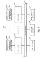
- data processing system 8 includes a number of processors 10a-10n , which each preferably comprise one of the PowerPCTM line of processors available from International Business Machines Corporation.
- processors 10a-10n also includes an associated one of on-board level one (L1) caches 12a-12n , which temporarily stores instructions and data that are likely to be accessed by the associated processor.
- L1 caches 12a-12n which temporarily stores instructions and data that are likely to be accessed by the associated processor.
- L1 caches 12a-12n are illustrated in Figure 1 as unified caches that store both instruction and data (both referred to hereinafter simply as data), those skilled in the art will appreciate that each of L1 caches 12a-12n could alternatively be implemented as bifurcated instruction and data caches.
- data processing system 8 also includes one or more additional levels of cache memory, such as level two (L2) caches 14a-14n, which are utilized to stage data to L1 caches 12a-12n.
- L2 caches 14a-14n function as intermediate storage between system memory 18 and L1 caches 12a-12n , and can typically store a much larger amount of data than L1 caches 12a-12n , but at a longer access latency
- L2 caches 14a-14n may have a storage capacity of 256 or 512 kilobytes
- L1 caches 12a-12n may have a storage capacity of 64 or 128 kilobytes.
- Figure 1 depicts only two levels of cache, the memory hierarchy of data processing system 8 could be expanded to include additional levels (L3, L4, etc.) of serially-connected or lookaside caches.
- data processing system 8 further includes I/O devices 20, system memory 18, and non-volatile storage 22, which are each coupled to interconnect 16 I/O devices 20 comprise conventional peripheral devices, such as a display device, keyboard, and graphical pointer, which are interfaced to interconnect 16 via conventional adapters.
- I/O devices 20 comprise conventional peripheral devices, such as a display device, keyboard, and graphical pointer, which are interfaced to interconnect 16 via conventional adapters.
- Non-volatile storage 22 stores an operating system and other software, which are loaded into volatile system memory 18 in response to data processing system 8 being powered on.
- data processing system 8 can include many additional components that are not shown in Figure 1, such as serial and parallel ports for connection to networks or attached devices, a memory controller that regulates access to system memory 18, etc.
- Interconnect 16 which can comprise one or more buses or a cross-point switch, serves as a conduit for communication transactions between L2 caches 14a-14n, system memory 18, input/output (I/O) devices 20, and non-volatile storage 22.
- a typical communication transaction on interconnect 16 includes a source tag indicating the source of the transaction, a destination tag specifying the intended recipient of the transaction, an address and/or data.
- Each device coupled to interconnect 16 preferably snoops all communication transactions on interconnect 16.
- L2 cache 14 is a four-way set associative cache that utilizes 32-bit addresses.
- data array 34 of L2 cache 14 comprises a number of congruence classes that each contain 4 ways for storing cache lines.
- memory locations in system memory 18 are mapped to particular congruence classes within data array 34 utilizing index bits within the address of the memory location (e.g., bits 20-26 of a 32-bit address).
- the cache lines stored within data array 34 are recorded in cache directory 32, which contains one directory entry for each way in data array 34.
- Each directory entry comprises a tag field 40, coherency status field 42, least recently used (LRU) field 44, and inclusion field 46.
- Tag field 40 specifies which cache line is stored in the corresponding way of data array 34 by storing the tag bits (e.g., bits 0-19) of the system memory address of the cache line.
- coherency status field 42 indicates the coherency status of the data stored in the corresponding way of data array 34 utilizing predefined bit combinations.
- LRU field 44 indicates how recently the corresponding way of data array 34 has been accessed relative to the other ways of its congruence class, thereby indicating which cache line should be cast out of the congruence class in response to a cache miss.
- inclusion field 46 indicates whether or not the cache line stored in the corresponding way of data array 34 is also stored in the associated L1 cache 12.
- L2 cache 14 further includes cache controller 36, which manages storage and retrieval of data within data array 34 and updates to cache directory 32 in response to signals received from the associated L1 cache 12 and transactions snooped on interconnect 16.
- cache controller 36 contains a read queue 50 and a write queue 52 from which cache controller 36 performs updates to cache directory 32 and accesses to data array 34.
- cache controller 36 places the read request in an entry within read queue 50.
- Cache controller 36 services the read request by supplying the requested data to the associated L1 cache 12 and thereafter removes the read request from read queue 50.
- cache controller 36 may snoop a transaction initiated by another of L2 caches 14a-14n indicating that a remote processor 10 intends to modify its local copy of a specified cache line. In response to snooping this transaction, cache controller 36 places a request to read cache directory 32 in read queue 50 in order to determine if the specified cache line is resident in data array 34. If so, cache controller 36 places an appropriate response on interconnect 16 and, if necessary, inserts a directory write request in write queue 52, that when serviced, updates the coherency status field associated with the specified cache line.
- Figure 2 illustrates an embodiment in which only one read queue and one write queue are utilized, it should be understood that the number of queues employed by cache controller 36 is a matter of design choice and that cache controller 36 may employ separate queues for cache directory accesses and data array accesses.
- Cache controller 36 further includes mode register 60, which, as described in greater detail below, comprises one or more bits whose settings control the operation of cache controller 36.
- cache controller 36 includes performance monitor 70.
- Performance monitor 70 is equipped with a number of performance monitor counters (PMC0-PMCn) 72 that, when enabled, increment in response to each occurrence of an event or combination of events specified by one or more control registers (CR0-CRm) 74.
- the events that may be counted by PMCs 72 in response to the settings of CRs 74 include cache hits, cache misses, the number of entries in a specified queue, access latency for L2 cache hits, access latency for L2 cache misses, etc.
- Each of PMCs 72 and CRs 74 are preferably memory mapped registers that may be read and written by the associated processor 10 via load and store instructions.
- the H-MESI protocol is preferably implemented only by the lowest level of cache in the memory hierarchy (e.g., L2 caches 14a-14n in the embodiment of data processing system 8 illustrated in Figure 1), while higher level caches preferably implement the conventional MESI protocol.
- the H-MESI protocol may be implemented at each level of cache in the memory hierarchy at the expense of additional inter-cache communication traffic.
- the H-MESI memory coherency protocol includes the conventional modified (M), exclusive (E), shared (S), and invalid (I) states of the MESI protocol, which are respectively identified by reference numerals 80, 82, 84, and 86.
- the H-MESI memory coherency protocol of the present invention includes hovering (H) state 90, which indicates that the address tag stored in the associated tag field 40 is valid but that the data item (e.g., cache line or cache sector) stored in the corresponding way of data array 34 is invalid.
- H hovering
- coherency status field 42 of each entry of each L2 cache directory 32 is initialized to I state 86 at power-on to indicate that both tag field 40 and the data stored in the corresponding way of data array 34 are invalid.
- L1 cache directory entries are similarly initialized to the invalid state according to the conventional MESI protocol. Thereafter, the coherency status of a cache line (or cache sector) stored in one of L2 caches 14a-14n in invalid state 86 can be updated to one of M state 80, E state 82, or S state 84, depending upon both the types of memory requests made by processors 10a-10n and the response of the memory hierarchy to those requests.
- L1 cache 12a makes a determination of whether or not the requested data is resident in L1 cache 12a. In response to a hit in L1 cache 12a, L1 cache 12a simply supplies the requested data to processor 10a. However, in response to miss in L1 cache 12a , L1 cache 12a forwards the read request to L2 cache 14a via inter-cache connections. In response to a hit in L2 cache 14a , the requested data is supplied by L2 cache 14a to L1 cache 12a, which stores the requested data in association with the appropriate MESI coherency status and forwards the requested data to processor 10a .
- cache controller 36 of L2 cache 14a presents the read request as a transaction on interconnect 16, which is snooped by each of L2 caches 14b-14n .
- cache controller 36 in each of L2 caches 14b-14n determines if the requested data is resident in its data array 34 or the associated one of L1 caches 12b-12n . If none of L2 caches 14b-14n or L1 caches 12b-12n stores the requested data, each of L2 caches 14a-14n returns a null response to L2 cache 14a, which then requests the data from system memory 18.
- cache controller 36 forwards the requested data to L1 cache 12a, stores the requested data in its data array 34, and updates the coherency status field 42 associated with the way storing the requested data from I state 86 to E state 82, as indicated by reference numeral 100.
- E state 82 indicates that the associated cache line is valid and is not resident in any other cache at the second level of the memory hierarchy.
- L2 cache 14a retrieves the requested data from system memory 18. In this case, however, the coherency status of the way in L2 cache 14a that stores the requested data makes a transition from I state 86 to S state 84, as indicated by reference numeral 102. Others of L2 caches 14 storing the requested data in E state 82 are also updated to S state 84, as indicated by reference numeral 104.
- cache controller 36 of L2 cache 14n responds to the read request with a retry and signals L1 cache 12n to push the requested data to memory.
- the coherency status of the requested data in L1 cache 12n and L2 cache 14n is then updated to S state 84 as indicated by reference numeral 106.
- L2 cache 14a retries the read request on interconnect 16
- L2 cache 14n replies with a shared response and L2 cache 14a obtains the requested data from system memory 18 as discussed above
- the requested data is sourced by cache controller 36 of L2 cache 14n rather than by system memory 18, thereby reducing access latency.
- L1 cache 12a issues a "read with intent to modify" request indicating that processor 10a desires to acquire exclusive use of a memory location for the purpose of modifying it
- L1 cache 12a stores the requested cache line in modified state.
- the "read with intent to modify" transaction indicates that other copies of the requested cache line will become stale
- the other L1 and L2 caches must indicate that their copies of the requested cache line are invalid. In L1 caches 12b-12n, any copies of the requested cache line are simply marked as invalid.
- each of L2 caches 14b-14n storing a copy of the requested cache line updates the coherency status field 42 associated with its copy from any of S state 84, M state 80, or E state 82 to H state 90, as indicated by reference numerals 110, 112, and 114, respectively.
- H state 90 indicates that the tag stored in tag field 40 remains valid, but that the associated cache line within data array 34 is invalid.
- Entries in a cache directory 32 are similarly updated to H state 90 in response to other snooped transactions that require data to be invalidated, including kills (i.e., transactions that explicitly invalidate a specified data block), flushes (i.e., transactions that invalidate a specified data block and copy any modified data to system memory), dclaims (i.e., transactions that invalidate copies of a cache line marked as shared in remote caches in response to a local copy of the cache line becoming modified in response to a store), etc.
- kills i.e., transactions that explicitly invalidate a specified data block
- flushes i.e., transactions that invalidate a specified data block and copy any modified data to system memory
- dclaims i.e., transactions that invalidate copies of a cache line marked as shared in remote caches in response to a local copy of the cache line becoming modified in response to a store
- a cache directory entry can make a transition from H state 90 to E state 82, M state 80, or S state 84, depending upon what type of transactions are received by the cache.
- a directory entry of L2 cache 14a that is in H state 90 makes a transition to E state 82 (as indicated by reference numeral 86) in response to processor 10a making a read request that (after missing in both L1 cache 12a and L2 cache 14a) receives a null response from L2 caches 14b-14n since the data retrieved from system memory 18 will, of all L2 caches 14a-14n, be stored only in L2 cache 14a.
- processor 10a indicates an intent to store data to a way of L1 cache 12a that is in H state 90
- L1 cache 12a indicates that intent to L2 cache 14a, which then issues a "read with intent to modify" transaction on interconnect 16.
- copies of the requested cache line stored in L2 caches 14b-14n are updated to H state 90 in response to snooping the "read with intent to modify" transaction, and copies of the requested cache line stored in L1 caches 12b-12n are marked as invalid.
- the cache line is marked as modified in L1 cache 12a to signify that the cache line is valid, but is not coherent with system memory 18 .
- the modified cache line may subsequently be stored in L2 cache 14a (e.g., in response to an L1 castout) without the modified cache line being written back to system memory 18. If so, the coherency status field 42 in L2 cache 14a associated with the modified cache line is updated to M state 80, as indicated by reference numeral 118 . Finally, an L2 cache directory entry in H state 90 is updated to S state 84 in response to a number of different request/response scenarios.
- an L2 directory entry in H state 90 transitions to S state 84 when the associated processor 10 issues a read request to the address indicated by the (valid) address tag in tag field 40 and at least one L2 cache 14 replies with a shared response. More importantly, an L2 directory entry in H state 90 can be updated to S state 84 without the associated processor 10 issuing a data request or the L2 cache 14 initiating a transaction on interconnect 16. As described above, each of L2 caches 14a-14n snoops all transactions issued on interconnect 16.
- L2 cache 14a-14n snoops a transaction issued by another of L2 caches 14b-14n that includes an updated (i.e., valid) copy of data that is stored in L2 cache 14a in H state 90
- cache controller 36 of L2 cache 14a samples the data from interconnect 16, stores the snooped data in data array 34, and updates the associated coherency status field 42 from H state 90 to S state 84.
- L2 cache 14a also provides a response to the snooped transaction, if a response is required to maintain coherency.
- L2 cache 14a must provide a shared response indicating its intention to sample the requested data so that the requesting L2 cache stores the requested data in S state 84 rather than E state 82.
- Transactions on interconnect 16 that can be snooped in this way to refresh invalid data associated with a valid address tag include read transactions, write transactions, data writebacks to system memory 18 due to cache line castouts, etc.
- the H-MESI protocol can be implemented either precisely or imprecisely.
- a precise implementation of the H-MESI protocol requires that L2 caches 14a-14n always sample data available on interconnect 16 to refresh invalid cache lines in H state 90.
- an imprecise implementation permits L2 caches 14a-14n to selectively sample data on interconnect 16 to refresh cache lines in H state 90 .
- each L2 cache 14 can, independently of the other L2 caches, operate in either a precise mode or an imprecise mode based upon the state of mode bit 62 in its mode register 60.
- L2 caches 14a-14n in precise mode is particularly advantageous when debugging or performance-tuning software because the precise mode of operation promotes more predictable software behavior and consistent software timing.
- data requests that miss at both levels of local cache are typically rare and can therefore serve as indications of possible "bugs" in the software.
- the precise H-MESI protocol guarantees that data that is requested by a processor 10 and is stored in the local L2 cache 14 in H state 90 will always be sourced by modified intervention (i.e., fast).
- a chief disadvantage of operating an L2 cache 14 in the precise mode is that snooped transactions capable of updating an L2 cache line in H state 90 must be retried if the update cannot be performed, for example, due to write queue 52 of the L2 cache 14 being full (i.e., busy).
- L2 caches 14a-14n are in the imprecise mode during normal operation.
- the imprecise mode of operation permits updates to cache lines in H state 90 to be performed selectively.
- updates to cache lines in H state 90 are performed only if write queue 52 (or a dedicated directory write queue, if implemented) has less than a threshold number of entries.
- either hardware within the L2 cache 14 or software executed by the associated processor 10 can be used to set mode bit 62 to the state corresponding to the imprecise mode in response to the number of entries in write queue 52 exceeding a predetermined threshold.
- other embodiments of the present invention may selectively perform updates to L2 cache lines in H state 90 based on other criteria, as described in detail below.
- each of L2 caches 14a-14n can independently be set to precise mode or imprecise mode by either software or hardware or both.
- processor 10a can simply set mode bit 62 by executing a store instruction that targets mode register 60.
- software can store values to CRs 74 that cause PMCs 72 to count occurrences of events of interest, such as the insertion and removal of entries in write queue 52, L2 accesses, L2 cache misses, access latency on L2 cache misses, etc.
- the software can then access the values in the PMCs 72 of interest by executing load instructions.
- the software can set mode bit 62 to select the appropriate one of the precise and imprecise modes. For example, if L2 cache 14a is operating in the imprecise mode and the number of L2 cache misses is greater than a predetermined percentage of the total number of L2 accesses, software can set mode bit 62 to the state corresponding to the precise mode.
- each performance monitor 70 includes logic for generating a signal that sets mode bit 62 to a specified state in response to the number of occurrences of a selected event or combination of events accumulated in one or more of PMCs 72 exceeding a predetermined threshold.
- the selection of the event or events of interest and the enablement of PMCs 72 can be determined either by default settings of performance monitor 70 or by software executed by the associated processor 10.
- performance monitor 70 can be set to generate a performance monitor interrupt (PMI) in response to the number of occurrences of a selected event or combination of events exceeding a predetermined threshold.
- the PMI is serviced by the associated processor 10, which executes an interrupt handler that changes the state of mode bit 62
- the present invention provides an improved method and system for maintaining memory coherency in a multiprocessor data processing system.
- the improved memory coherency protocol provided by the present invention permits an invalid data item stored within a cache in association with a valid address tag to be automatically updated with valid data without the associated processor issuing an explicit read or write request.
- data invalidated by the activity of remote processors can be refreshed prior to the data being accessed by the local processor, thereby substantially reducing access latency by eliminating the need to retrieve the data from a remote cache or system memory.
- Contention for memory access and system-wide locks is also substantially reduced since cache lines are updated without accessing memory or requesting a lock.
- FIG. 3 The illustrative embodiment of a memory coherency protocol depicted in Figure 3 could be modified by eliminating I state 86 because that state is only utilized to initialize directory entries at power-on and is never re-entered from another state. If I state 86 were eliminated, at power-on the coherency status field of each L2 directory entry would be initialized to H state 90, and the tag field of each L2 directory entry would be initialized to a tag value that is unique at least within the same congruence class.
- performance monitor 70 of Figure 2 could alternatively be implemented as a single system-wide performance monitor coupled to interconnect 16 rather than as multiple separate performance monitors internal to each L2 cache 14.
Landscapes
- Engineering & Computer Science (AREA)
- Theoretical Computer Science (AREA)
- Physics & Mathematics (AREA)
- General Engineering & Computer Science (AREA)
- General Physics & Mathematics (AREA)
- Memory System Of A Hierarchy Structure (AREA)
Claims (15)
- Procédé d'entretien de la cohérence des antémémoires dans un système de traitement de données comprenant une pluralité de processeurs (10a à 10n) qui sont reliés à une interconnexion (16), chacun étant associé à une antémé moire respective d'une pluralité d'antémémoires (14a à 14n), ledit procédé comprenant les étapes consistant à,mémoriser, dans une première antémémoire (14a) parmi ladite pluralité d'antémémoires, un premier élément de données en association avec une étiquette d'adressage (40) indiquant une adresse dudit premier élément de donnée s,établir un indicateur de cohérence (42) dans ladite première antémémoire dans un premier état (82), qui indique que ledit premier élément de données est valide,mettre à jour ledit indicateur de cohérence dans ladite première antémémoire dans un second état (90) qui indique que ladite étiquette d'adressage est valide et que ledit élément de données dans ladite première antémémo ire est invalide, en réponse à une autre antémémoire de ladite pluralité d'antémémoires indiquant une intention de mémoriser à ladite adresse indiquée par ladite étiquett e d'adressage alors que ledit indicateur de cohérence est tabli dans ledit premier état,ledit procédé étant caractérisé par les étapes consistantdéterminer, en réponse à un mode de fonctionnement de ladite première antémémoire, s'il faut ou non mettre à jour ladite première antémémoire, en réponse à une détecti on d'un transfert de données sur ladite interconnexion associé à ladite adresse indiquée par ladite étiquette d'adressage alors que ledit indicateur de cohérence est ét abli dans ledit second état, ledit transfert de données ét ant lancé par une autre antémémoire de ladite pluralité d'antémémoires et comprenant un second élément de données, etremplacer ledit premier élément de données en mémorisant ledit second élément de données dans ladite première antémémoire en association avec ladite étiquette d'adressage et en mettant à jour ledit indicateur de cohér ence dans un troisième état (84) qui indique que ledit second élément de données est valide, en réponse à une dét ermination pour réaliser une mise à jour dans ladite premire antémémoire.
- Antémémoire destinée à permettre une cohérence des antémémoires dans un système de traitement de données comprenant une pluralité de processeurs (10a à 10n) qui sont reliés à une interconnexion (16) et chacun étant associé à une antémémoire respective d'une pluralité d'antmémoires (14a à 14n), ladite antémémoire comprenant :une mémoire de données (34) destinée à mémoriser un élémen t de données,une mémoire d'étiquettes (40) destinée à mémoriser une étiquette d'adressage indiquant une adresse dudit élément de données contenu dans ladite mémoire de données,un moyen destiné à établir un indicateur de cohérence (42) dans un premier état (82) qui indique que ledit éléme nt de données est valide en réponse au fait que ledit élém ent de données est mémorisé dans ladite mémoire de données et un moyen destiné à établir l'indicateur de cohérence dans un second état ( 90) en réponse à une autre antémémoire de la pluralité des antémémoires indiquant une intention de mémoriser à ladite adresse indiquée par ladite étiquette d'adressage alors que ledit indicateur de cohérence est établi dans ledit premier éta t, ledit second état dudit indicateur de cohérence indiquant que ladite étiquette d'adressage est valide et que ledit élémen t de données dans ladite mémoire de données est invalide,ladite antémémoire étant caractérisée en ce qu'elle comprend en outre :un moyen, répondant à la détection d'un transfert de données sur ladite interconnexion associé à ladite adresse indiquée par ladite étiquette d'adressage alors que ledit indicateur de cohérence est établi dans ledit second état (90), ledit transfert de données étant lancé par une autre antémémoire de ladite pluralité d'antémémoir es et comprenant un second élément de données, destiné à dterminer, en réponse à un mode de fonctionnement de ladite première antémémoire, s'il faut ou non mettre à jour ladite première antémémoire, etun moyen, répondant à une détermination pour réaliser une mise à jour dans ladite première antémémoire, destiné remplacer ledit premier élément de données en mémorisant ledit second élément de données dans ladite première antém moire en association avec ladite étiquette d'adressage et destiné à mettre à jour ledit indicateur de cohérence dans un troisième état (84) qui indique que ledit second é lément de données est valide.
- Système de traitement de données destiné à entretenir une cohérence des antémémoires comprenant une interconnexion (16), une pluralité de processeurs (10a à 10n) reliés à ladite interconnexion, une pluralité d'antém moires (14a à 14n) qui sont chacune associées à un processeur respectif de la pluralité de processeurs,dans lequel une première antémémoire parmi ladite pluralité d'antémémoires comprend une mémoire de données (34) destinée à mémoriser un élément de données, une mémoi re d'étiquettes (40) destinée à mémoriser une étiquette d'adressage indiquant une adresse dudit élément de données contenu dans ladite mémoire de données, un moyen destiné établir un indicateur de cohérence (42) dans un premier é tat (82) qui indique que ledit élément de données est valide en réponse au fait que ledit élément de données est mémorisé dans ladite mémoire de données et un moyen destiné à établir l'indicateur de cohérence dans un second état (90) en réponse au fait qu'une autre antémémoi re de la pluralité d'antémémoires indique une intention de mémoriser à ladite adresse indiquée par ladite étiquett e d'adressage alors que ledit indicateur de cohérence est tabli dans ledit premier état, ledit second état dudit indicateur de cohérence indiquant que ladite étiquette d'adressage est valide et que ledit élément de données dans ladite mémoire de données est invalide, ledit système de traitement de données étant caractérisé en ce que ladite première antémémoire comprend en outre un moyen, ré pondant à la détection d'un transfert de données sur ladite interconnexion associé à ladite adresse indiquée par ladite étiquette d'adressage alors que ledit indicateur de cohérence est établi dans ledit second état, ledit transfert de données étant lancé par une autre anté mémoire de ladite pluralité d'antémémoires et comprenant un second élément de données, af in de déterminer, en réponse à un mode de fonctionnement de ladite première antémémoire, s'il faut ou non mettre à jour ladite première antémémoire, et un moyen, répondant à une détermination pour effectuer une mise à jour dans ladite premiè re antémémoire, afin de remplacer ledit premier élément de donnes en mémorisant ledit second élément de données dans ladite première antémémoire en association avec ladite étiquette d'adressage et afin de mettre à jour ledit indicateur de cohérence dans un troisième état (84) qui indique que ledit second lément de données est valide.
- Procédé selon la revendication 1, caractérisé en ce que ladite étape de détermination, en réponse à un mode de fonctionnement de ladite première antémémoire, du fait qu'il faut mettre à jour ou non ladite première antémémoir e comprend les étapes consistant à : si ladite première antémémoire fonctionne dans un premier mode, décider toujours de mettre à jour ladite première antémémoire, et si ladite première antémémoire fonctionne dans un second mode, décider de mettre à jour ladite première antémémoire uniquement en réponse à une absence d'une condition sélec tionnée à l'intérieur de ladite première antémémoire.
- Procédé selon la revendication 4, caractérisé en ce que ladite première antémémoire comprend une file d'attente à partir de laquelle des mises à jour vers ladite première antémémoire sont faites, lesdites étapes consistant à décider de mettre à jour ladite première anté mémoire uniquement en réponse à une absence d'une condition sélectionnée à l'intérieur de ladite première antémémoire comprend une étape consistant à décider de mettre à jour ladite première antémémoire uniquement si ladite file d'attente contient moins qu'un nombre seuil d'entrées.
- Procédé selon la revendication 1, caractérisé en ce qu'il comprend une étape consistant à établir ledit mode de fonctionnement de ladite première antémémoire dans l'un d'un premier mode et d'un second mode en réponse à une instruction exécutée par un premier processeur parmi ladite pluralité de processeurs.
- Procédé selon la revendication 1, caractérisé en ce qu'il comprend une étape de surveillance par un matériel de surveillance de performances, de un ou plusieurs événem ents sélectionnés et consistant à établir ledit mode de fonctionnement de ladite première antémémoire en réponse à une occurrence d'au moins un événement parmi lesdits un ou plusieurs événements sélectionnés, dans lequel l'étape consistant à établir ledit mode de fonctionnement de ladite première antémémoire utilise ledit matériel de surveillance de performances.
- Procédé selon la revendication 1, caractérisé en ce que ladite étape de mise à jour dudit indicateur de cohére nce dans un troisième état qui indique que ledit second él ment de données est valide comprend l'étape consistant à mettre à jour ledit indicateur de cohérence dans un état partagé qui indique que ledit second élément de données est mémorisé à la fois dans ladite première antémémoire et une autre antémémoire de ladite pluralité d'antémémoire s.
- Procédé selon la revendication 1, caractérisé en ce que ladite étape consistant à établir un indicateur de cohrence dans ladite première antémémoire dans un premier tat qui indi que que ledit élément de données est valide comprend l'étape consistant à établir ledit indicateur de cohérence dans ladite première antémémoire dans l'un d'un état modifié, d'un é tat partagé, et d'un état exclusif.
- Antémémoire selon la revendication 2 ou système selon la revendication 3, caractérisé en ce que ledit moyen destiné à déterminer, en réponse à un mode de fonctionnement de ladite première antémémoire, s'il faut ou non mettre à jour ladite première antémémoire comprend un moyen destiné à décider toujours de mettre à jour ladite première antémémoire, si ladite première antémémoir e fonctionne dans un premier mode et un moyen destiné à dé cider de mettre à jour ladite première antémémoire uniquement en réponse à une absence d'une condition sélect ionnée à l'intérieur de ladite première antémémoire si ladite première antémémoire fonctionne dans un second mode.
- Antémémoire ou système selon la revendication 10, caractérisé en ce que ladite première antémémoire comprend une file d'attente à partir de laquelle des mises à jour sont faites dans ladite première antémémoire, et ledit moyen destiné à décider de mettre à jour ladite première antémémoire uniquement en réponse à une absence d'une condition sélectionnée à l'intérieur de ladite premire antémémoire, comprend un moyen destiné à décider de mettre à jour ladite première antémémoire uniquement si ladite file d'attente contient moins qu'un nombre seuil d'entrées.
- Antémémoire selon la revendication 2, ou système selon la revendication 3, caractérisé en ce qu'il comprend un moyen destiné à établir ledit mode de fonctionnement de ladite première antémémoire dans l'un d'un premier mode et d'un second mode en réponse à une instruction exécutée par un premier processeur parmi ladite pluralité de processeurs.
- Antémémoire selon la revendication 2, ou système selon la revendication 3, caractérisé en ce qu'il comprend un matériel de surveillance de performances destiné à surveiller un ou plusieurs événements sélectionn s et destiné à établir ledit mode de fonctionnement de ladite première antémémoire en réponse à une occurrence d'au moins un événement parmi lesdits un ou plusieurs évén ements sélectionnés.
- Antémémoire selon la revendication 2 ou système selon la revendication 3, caractérisé en ce que ledit moyen destiné à mettre à jour ledit indicateur de cohérenc e dans un troisième état qui indique que ledit second élément de données est valide, comprend un moyen destiné à mettre à jour ledit indicateur de cohérence dans un état partagé qui indique que ledit second élément de données est mémorisé à la fois dans ladite première antémémoire et une autre antémémoire de ladite pluralité d'antémémoires.
- Antémémoire selon la revendication 2 ou système selon la revendication 3, caractérisé en ce que ledit moyen destiné à établir un indicateur de cohérence dans ladite première antémémoire dans un premier état qui indique que ledit élément de données est valide comprend un moyen destiné à établir ledit indicateur de cohérence dans ladite première antémémoire à l'un d'un état modifié, d'un état partagé, et d'un état exclusif.
Applications Claiming Priority (2)
| Application Number | Priority Date | Filing Date | Title |
|---|---|---|---|
| US24612 | 1998-02-17 | ||
| US09/024,612 US6263407B1 (en) | 1998-02-17 | 1998-02-17 | Cache coherency protocol including a hovering (H) state having a precise mode and an imprecise mode |
Publications (3)
| Publication Number | Publication Date |
|---|---|
| EP0936554A2 EP0936554A2 (fr) | 1999-08-18 |
| EP0936554A3 EP0936554A3 (fr) | 2000-01-26 |
| EP0936554B1 true EP0936554B1 (fr) | 2001-12-19 |
Family
ID=21821494
Family Applications (1)
| Application Number | Title | Priority Date | Filing Date |
|---|---|---|---|
| EP99301056A Expired - Lifetime EP0936554B1 (fr) | 1998-02-17 | 1999-02-15 | Protocole de cohérence d'antémémoire avec un état en suspens (H) ayant un mode précis et un mode imprécis |
Country Status (9)
| Country | Link |
|---|---|
| US (1) | US6263407B1 (fr) |
| EP (1) | EP0936554B1 (fr) |
| JP (1) | JP3277171B2 (fr) |
| KR (1) | KR100330934B1 (fr) |
| CN (1) | CN1131481C (fr) |
| DE (1) | DE69900611T2 (fr) |
| ID (1) | ID22046A (fr) |
| MY (1) | MY122483A (fr) |
| TW (1) | TW426824B (fr) |
Families Citing this family (20)
| Publication number | Priority date | Publication date | Assignee | Title |
|---|---|---|---|---|
| JP2000330965A (ja) * | 1999-03-17 | 2000-11-30 | Hitachi Ltd | マルチプロセッサシステム及びそのメモリアクセストランザクションの転送方法 |
| US6349369B1 (en) * | 1999-11-09 | 2002-02-19 | International Business Machines Corporation | Protocol for transferring modified-unsolicited state during data intervention |
| US6345344B1 (en) * | 1999-11-09 | 2002-02-05 | International Business Machines Corporation | Cache allocation mechanism for modified-unsolicited cache state that modifies victimization priority bits |
| US6345343B1 (en) * | 1999-11-09 | 2002-02-05 | International Business Machines Corporation | Multiprocessor system bus protocol with command and snoop responses for modified-unsolicited cache state |
| US6374333B1 (en) * | 1999-11-09 | 2002-04-16 | International Business Machines Corporation | Cache coherency protocol in which a load instruction hint bit is employed to indicate deallocation of a modified cache line supplied by intervention |
| US6345342B1 (en) * | 1999-11-09 | 2002-02-05 | International Business Machines Corporation | Cache coherency protocol employing a read operation including a programmable flag to indicate deallocation of an intervened cache line |
| US6925634B2 (en) * | 2001-01-24 | 2005-08-02 | Texas Instruments Incorporated | Method for maintaining cache coherency in software in a shared memory system |
| US7194586B2 (en) * | 2002-09-20 | 2007-03-20 | International Business Machines Corporation | Method and apparatus for implementing cache state as history of read/write shared data |
| US7496715B1 (en) * | 2003-07-16 | 2009-02-24 | Unisys Corporation | Programmable cache management system and method |
| US7225299B1 (en) | 2003-07-16 | 2007-05-29 | Transmeta Corporation | Supporting speculative modification in a data cache |
| KR100515059B1 (ko) * | 2003-07-22 | 2005-09-14 | 삼성전자주식회사 | 멀티프로세서 시스템 및 멀티프로세서 시스템의 캐쉬일관성 유지 방법 |
| US9727468B2 (en) * | 2004-09-09 | 2017-08-08 | Intel Corporation | Resolving multi-core shared cache access conflicts |
| US7376798B1 (en) | 2005-04-07 | 2008-05-20 | Transmeta Corporation | Memory management methods and systems that support cache consistency |
| JP4784928B2 (ja) * | 2005-08-24 | 2011-10-05 | 株式会社リコー | 情報処理装置、情報処理システム、情報処理方法、及び、情報処理プログラムとその記録媒体 |
| US8327075B2 (en) * | 2005-12-08 | 2012-12-04 | International Business Machines Corporation | Methods and apparatus for handling a cache miss |
| US7571286B2 (en) * | 2006-08-24 | 2009-08-04 | International Business Machines Corporation | Reduced memory traffic via detection and tracking of temporally silent stores |
| US8874855B2 (en) | 2009-12-28 | 2014-10-28 | Empire Technology Development Llc | Directory-based coherence caching |
| CN102122256B (zh) * | 2011-03-28 | 2013-01-09 | 中国人民解放军国防科学技术大学 | 一种用于进程间通信的管道式通信方法及系统 |
| US20170255569A1 (en) * | 2016-03-01 | 2017-09-07 | Qualcomm Incorporated | Write-allocation for a cache based on execute permissions |
| CN110443360B (zh) * | 2017-06-16 | 2021-08-06 | 上海兆芯集成电路有限公司 | 用于操作处理器的方法 |
Family Cites Families (24)
| Publication number | Priority date | Publication date | Assignee | Title |
|---|---|---|---|---|
| US4755930A (en) | 1985-06-27 | 1988-07-05 | Encore Computer Corporation | Hierarchical cache memory system and method |
| DE68917326T2 (de) | 1988-01-20 | 1995-03-02 | Advanced Micro Devices Inc | Organisation eines integrierten Cachespeichers zur flexiblen Anwendung zur Unterstützung von Multiprozessor-Operationen. |
| JPH0680499B2 (ja) | 1989-01-13 | 1994-10-12 | インターナショナル・ビジネス・マシーンズ・コーポレーション | マルチプロセッサ・システムのキャッシュ制御システムおよび方法 |
| US5119485A (en) * | 1989-05-15 | 1992-06-02 | Motorola, Inc. | Method for data bus snooping in a data processing system by selective concurrent read and invalidate cache operation |
| US5287484A (en) | 1989-06-21 | 1994-02-15 | Hitachi, Ltd. | Multi-processor system for invalidating hierarchical cache |
| JPH061463B2 (ja) | 1990-01-16 | 1994-01-05 | インターナショナル・ビジネス・マシーンズ・コーポレーション | マルチプロセッサ・システムおよびそのプライベート・キャッシュ制御方法 |
| JP2820752B2 (ja) | 1990-01-19 | 1998-11-05 | 日本電信電話株式会社 | 密結合マルチプロセッサシステムにおけるキャッシュメモリ一致制御方法 |
| JPH0625984B2 (ja) | 1990-02-20 | 1994-04-06 | インターナシヨナル・ビジネス・マシーンズ・コーポレーシヨン | マルチプロセツサ・システム |
| CA2051209C (fr) | 1990-11-30 | 1996-05-07 | Pradeep S. Sindhu | Protocoles de coherence pour multiprocesseurs a memoire commune |
| US5282272A (en) | 1990-12-21 | 1994-01-25 | Intel Corporation | Interrupt distribution scheme for a computer bus |
| EP0553743A1 (fr) | 1992-01-31 | 1993-08-04 | Motorola, Inc. | Contrôleur d'antémémoire |
| US5319766A (en) * | 1992-04-24 | 1994-06-07 | Digital Equipment Corporation | Duplicate tag store for a processor having primary and backup cache memories in a multiprocessor computer system |
| JPH06110844A (ja) | 1992-08-11 | 1994-04-22 | Toshiba Corp | 分散共有メモリ型マルチプロセッサシステム |
| JP3013631B2 (ja) | 1992-09-28 | 2000-02-28 | 日本電気株式会社 | キャッシュメモリ同期方法 |
| US5522057A (en) | 1993-10-25 | 1996-05-28 | Intel Corporation | Hybrid write back/write through cache having a streamlined four state cache coherency protocol for uniprocessor computer systems |
| US5671391A (en) | 1994-01-10 | 1997-09-23 | Ncr Corporation | Coherent copyback protocol for multi-level cache memory systems |
| US5588131A (en) | 1994-03-09 | 1996-12-24 | Sun Microsystems, Inc. | System and method for a snooping and snarfing cache in a multiprocessor computer system |
| US5666509A (en) | 1994-03-24 | 1997-09-09 | Motorola, Inc. | Data processing system for performing either a precise memory access or an imprecise memory access based upon a logical address value and method thereof |
| DE69519816T2 (de) | 1994-05-03 | 2001-09-20 | Hewlett-Packard Company (A Delaware Corporation), Palo Alto | Anordnung mit Duplikat des Cache-Etikettenspeichers |
| CA2148186A1 (fr) | 1994-05-04 | 1995-11-05 | Michael T. Jackson | Carte de traitement a antememoire de reinscription de deuxieme niveau et a antememoire a double ecriture de troisieme niveau qui conserve une information exclusive ppour un systeme informatique multiprocesseur |
| US5551001A (en) * | 1994-06-29 | 1996-08-27 | Exponential Technology, Inc. | Master-slave cache system for instruction and data cache memories |
| US6038644A (en) | 1996-03-19 | 2000-03-14 | Hitachi, Ltd. | Multiprocessor system with partial broadcast capability of a cache coherent processing request |
| US5900016A (en) | 1997-04-02 | 1999-05-04 | Opti Inc. | System for using a cache memory with a write-back architecture |
| US6049849A (en) * | 1997-04-14 | 2000-04-11 | International Business Machines Corporation | Imprecise method and system for selecting an alternative cache entry for replacement in response to a conflict between cache operation requests |
-
1998
- 1998-02-17 US US09/024,612 patent/US6263407B1/en not_active Expired - Fee Related
-
1999
- 1999-01-15 CN CN99101099A patent/CN1131481C/zh not_active Expired - Fee Related
- 1999-01-15 MY MYPI99000163A patent/MY122483A/en unknown
- 1999-02-09 JP JP03163399A patent/JP3277171B2/ja not_active Expired - Fee Related
- 1999-02-10 TW TW088102030A patent/TW426824B/zh not_active IP Right Cessation
- 1999-02-11 KR KR1019990004879A patent/KR100330934B1/ko not_active Expired - Fee Related
- 1999-02-15 ID IDP990114D patent/ID22046A/id unknown
- 1999-02-15 DE DE69900611T patent/DE69900611T2/de not_active Expired - Lifetime
- 1999-02-15 EP EP99301056A patent/EP0936554B1/fr not_active Expired - Lifetime
Also Published As
| Publication number | Publication date |
|---|---|
| DE69900611D1 (de) | 2002-01-31 |
| KR100330934B1 (ko) | 2002-04-01 |
| EP0936554A2 (fr) | 1999-08-18 |
| KR19990072595A (ko) | 1999-09-27 |
| MY122483A (en) | 2006-04-29 |
| CN1131481C (zh) | 2003-12-17 |
| TW426824B (en) | 2001-03-21 |
| JP3277171B2 (ja) | 2002-04-22 |
| EP0936554A3 (fr) | 2000-01-26 |
| JPH11328025A (ja) | 1999-11-30 |
| CN1231444A (zh) | 1999-10-13 |
| US6263407B1 (en) | 2001-07-17 |
| DE69900611T2 (de) | 2002-08-22 |
| HK1022970A1 (en) | 2000-08-25 |
| ID22046A (id) | 1999-08-26 |
Similar Documents
| Publication | Publication Date | Title |
|---|---|---|
| US6192451B1 (en) | Cache coherency protocol for a data processing system including a multi-level memory hierarchy | |
| EP0936554B1 (fr) | Protocole de cohérence d'antémémoire avec un état en suspens (H) ayant un mode précis et un mode imprécis | |
| US8495308B2 (en) | Processor, data processing system and method supporting a shared global coherency state | |
| EP0936558B1 (fr) | Protocole de cohérence d'antémémoire avec états en suspens (H) et récents (R) | |
| US6405290B1 (en) | Multiprocessor system bus protocol for O state memory-consistent data | |
| US6345341B1 (en) | Method of cache management for dynamically disabling O state memory-consistent data | |
| US6615321B2 (en) | Mechanism for collapsing store misses in an SMP computer system | |
| KR101072174B1 (ko) | 능동적 프리페치들로 향상된 호버 상태를 실시하는 시스템 및 방법 | |
| US6415358B1 (en) | Cache coherency protocol having an imprecise hovering (H) state for instructions and data | |
| US6397303B1 (en) | Data processing system, cache, and method of cache management including an O state for memory-consistent cache lines | |
| EP0936556B1 (fr) | Protocole de cohérence d'antémémoire avec un état en suspens | |
| US6272603B1 (en) | Cache coherency protocol having hovering (H), recent (R), and tagged (T) states | |
| US6615320B2 (en) | Store collapsing mechanism for SMP computer system | |
| US6356982B1 (en) | Dynamic mechanism to upgrade o state memory-consistent cache lines | |
| KR19990072313A (ko) | 명령어및데이터를위한배회상태를가지는캐시코히어런시프로토콜 | |
| US6349368B1 (en) | High performance mechanism to support O state horizontal cache-to-cache transfers | |
| US20040030950A1 (en) | Apparatus for imprecisely tracking cache line inclusivity of a higher level cache | |
| HK1022970B (en) | Cache coherency protocol including a hovering (h) state having a precise mode and an imprecise mode |
Legal Events
| Date | Code | Title | Description |
|---|---|---|---|
| PUAI | Public reference made under article 153(3) epc to a published international application that has entered the european phase |
Free format text: ORIGINAL CODE: 0009012 |
|
| AK | Designated contracting states |
Kind code of ref document: A2 Designated state(s): DE FR GB IE |
|
| AX | Request for extension of the european patent |
Free format text: AL;LT;LV;MK;RO;SI |
|
| RIN1 | Information on inventor provided before grant (corrected) |
Inventor name: LEWIS, JERRY DON Inventor name: DODSON, JOHN STEVEN Inventor name: ARIMILLI, RAVI KUMAR |
|
| PUAL | Search report despatched |
Free format text: ORIGINAL CODE: 0009013 |
|
| AK | Designated contracting states |
Kind code of ref document: A3 Designated state(s): AT BE CH CY DE DK ES FI FR GB GR IE IT LI LU MC NL PT SE |
|
| AX | Request for extension of the european patent |
Free format text: AL;LT;LV;MK;RO;SI |
|
| 17P | Request for examination filed |
Effective date: 20000626 |
|
| AKX | Designation fees paid |
Free format text: DE FR GB IE |
|
| GRAG | Despatch of communication of intention to grant |
Free format text: ORIGINAL CODE: EPIDOS AGRA |
|
| 17Q | First examination report despatched |
Effective date: 20010228 |
|
| GRAG | Despatch of communication of intention to grant |
Free format text: ORIGINAL CODE: EPIDOS AGRA |
|
| GRAH | Despatch of communication of intention to grant a patent |
Free format text: ORIGINAL CODE: EPIDOS IGRA |
|
| GRAH | Despatch of communication of intention to grant a patent |
Free format text: ORIGINAL CODE: EPIDOS IGRA |
|
| GRAA | (expected) grant |
Free format text: ORIGINAL CODE: 0009210 |
|
| AK | Designated contracting states |
Kind code of ref document: B1 Designated state(s): DE FR GB IE |
|
| REG | Reference to a national code |
Ref country code: GB Ref legal event code: IF02 |
|
| REG | Reference to a national code |
Ref country code: IE Ref legal event code: FG4D |
|
| REF | Corresponds to: |
Ref document number: 69900611 Country of ref document: DE Date of ref document: 20020131 |
|
| ET | Fr: translation filed | ||
| PLBE | No opposition filed within time limit |
Free format text: ORIGINAL CODE: 0009261 |
|
| STAA | Information on the status of an ep patent application or granted ep patent |
Free format text: STATUS: NO OPPOSITION FILED WITHIN TIME LIMIT |
|
| 26N | No opposition filed | ||
| PGFP | Annual fee paid to national office [announced via postgrant information from national office to epo] |
Ref country code: GB Payment date: 20030203 Year of fee payment: 5 |
|
| PGFP | Annual fee paid to national office [announced via postgrant information from national office to epo] |
Ref country code: FR Payment date: 20030217 Year of fee payment: 5 |
|
| PG25 | Lapsed in a contracting state [announced via postgrant information from national office to epo] |
Ref country code: GB Free format text: LAPSE BECAUSE OF NON-PAYMENT OF DUE FEES Effective date: 20040215 |
|
| GBPC | Gb: european patent ceased through non-payment of renewal fee |
Effective date: 20040215 |
|
| PG25 | Lapsed in a contracting state [announced via postgrant information from national office to epo] |
Ref country code: FR Free format text: LAPSE BECAUSE OF NON-PAYMENT OF DUE FEES Effective date: 20041029 |
|
| REG | Reference to a national code |
Ref country code: FR Ref legal event code: ST |
|
| PGFP | Annual fee paid to national office [announced via postgrant information from national office to epo] |
Ref country code: IE Payment date: 20090212 Year of fee payment: 11 |
|
| REG | Reference to a national code |
Ref country code: IE Ref legal event code: MM4A |
|
| PG25 | Lapsed in a contracting state [announced via postgrant information from national office to epo] |
Ref country code: IE Free format text: LAPSE BECAUSE OF NON-PAYMENT OF DUE FEES Effective date: 20100215 |
|
| PGFP | Annual fee paid to national office [announced via postgrant information from national office to epo] |
Ref country code: DE Payment date: 20180201 Year of fee payment: 20 |
|
| REG | Reference to a national code |
Ref country code: DE Ref legal event code: R071 Ref document number: 69900611 Country of ref document: DE |