EP0933872A1 - Optical digital holding apparatus - Google Patents
Optical digital holding apparatus Download PDFInfo
- Publication number
- EP0933872A1 EP0933872A1 EP99107155A EP99107155A EP0933872A1 EP 0933872 A1 EP0933872 A1 EP 0933872A1 EP 99107155 A EP99107155 A EP 99107155A EP 99107155 A EP99107155 A EP 99107155A EP 0933872 A1 EP0933872 A1 EP 0933872A1
- Authority
- EP
- European Patent Office
- Prior art keywords
- optical
- signal
- light
- input
- selector
- Prior art date
- Legal status (The legal status is an assumption and is not a legal conclusion. Google has not performed a legal analysis and makes no representation as to the accuracy of the status listed.)
- Ceased
Links
Images


Classifications
-
- H—ELECTRICITY
- H03—ELECTRONIC CIRCUITRY
- H03K—PULSE TECHNIQUE
- H03K3/00—Circuits for generating electric pulses; Monostable, bistable or multistable circuits
- H03K3/02—Generators characterised by the type of circuit or by the means used for producing pulses
- H03K3/42—Generators characterised by the type of circuit or by the means used for producing pulses by the use, as active elements, of opto-electronic devices, i.e. light-emitting and photoelectric devices electrically- or optically-coupled
Definitions
- the present invention relates to an optical digital holding apparatus for holding instantaneous digital information borne by an optical signal.
- An optical digital holding apparatus of the present invention carries out functions of a flip-flop apparatus (RS flip-flop, D-type flip-flop etc.) which is a kind of the electrical digital holding apparatus, and can be achieved by placing an optical connecting wiring having a direct or indirect feedback circuit which is the essence of the flip-flop circuit between the multistage optical selectors having the selector function.
- a flip-flop apparatus RS flip-flop, D-type flip-flop etc.
- the optical digital holding apparatus of the present invention comprises (a) a set of selectors for receiving an aggregation of spatially distributed optical digital information signals propagating in a predetermined direction and bearing binary digital information and an optical control signal bearing binary digital information and selectively outputting one of a portion of an aggregation of the digital information signals which are received in accordance with a value of the digital information borne by the optical control signal, having a delay function and an integration function, placed in multistage, and (b) an optical connection wiring for connecting the selectors each other, including optical feedback connection for making an output optical signal of one of the selectors into an input optical signal of one of the other selectors and making an output optical signal of one of the other selectors into its input signal or an input signal of a selector in a stage prior to said one of the other selectors.
- the number of optical digital information signals inputting to the selection is two and the number of said optical control signal is one.
- aforesaid selector outputs a third optical information signal bearing the binary digital information borne by either a first optical information signal received in a first area or a second optical information signal received in a second area in accordance with the value of the binary digital information borne by the optical control information.
- Such a selector is constructed in one of three ways hereunder in order to attain a high speed response.
- a first type of the selector comprises (1) a first variable transmittance (or reflectance) device and a second variable transmittance (or reflectance) device driven independently for controlling either the transmission (or reflection) of an input light or non-transmission (or non-reflection) of the light in accordance with an electric drive manner, (2) a first electric charge injecting device and a first electric charge discharging device, which are connected to the first variable transmittance (or reflectance) device, (3) a second electric charge injecting device and a second electric charge discharging device, which are connected to the second variable transmittance (or reflectance) device, and (4) an optical detection circuit for receiving the optical control signal, issuing an activation direction to either a first pair of the first electric charge injecting device and the second electric charge discharging device or a second pair of the second electric charge injecting device and the first electric charge discharging device, and issuing a deactivation direction to the other pairs in accordance with the value of the binary digital information carried by the optical control signal.
- a second type of the selector comprises (1) a first polarization plane rotation device for selectively conducting either non-rotation or 90 degrees rotation of a polarization direction of an input linearly polarized light having a predetermined direction of polarization, (2) a double refraction plate for changing an optical path in accordance with the direction of polarization of the input linearly polarized light received through the first polarization plane rotation device, (3) a second polarization plane rotation device for selectively conduction either the non-rotation or the 90 degrees rotation of the direction of polarization of the linearly polarized light outputted from the double refraction plate, (4) a polarization plane rotation controller for setting the first polarization plane rotation device and the second polarization plane rotation device into one of a non-rotation mode and a 90 degrees rotation mode in accordance with the value of the binary digital information carried by the optical control signal, and (5) an output light selector for selecting only the light outputted from a predetermined area of the second polarization plane rotation device.
- a third type of the selector comprises (1) a variable refractive index device for electrically changing a refractive index, (2) a refractive index controller for receiving the optical control signal and changing a refractive index of the variable refractive index device in accordance with the value of information carried by the optical control signal, and (3) a light selection slit for transmitting only a light outputted from a specified position of the variable refractive index device.
- the variable refractive index device is made of material what is called electro optical crystal.
- the holding function is achieved by a way such that an output optical signal of the optical selector in a preceding stage is made into an light selection signal or an input optical data signal, of the optical selector in a succeeding stage, and an output optical signal of the optical selector in the succeeding stage is made into an input optical data information or an light selection signal, of the optical selector itself in the succeeding stage or the optical selector placed in the stage prior to the selector in the succeeding stage.
- the optical selectors capable of being cascade-connected are placed in multistage and optically connected each other, so that the optical digital holding apparatus itself can also be cascade-connected. Further, by combining these with another optical digital processor, a large scale optical digital apparatus such as a counter, a shift register can be achieved.
- variable transmittance devices or variable reflectance devices having the quantum confined Stark effect or the Wannier-Stark localization effect are combined and driving transistors are prepared for the injection/discharge of the electric charges of the devices controlling the transmission/non-transmission of the light in the respective devices such that one is in the electric charge injection mode while the other is in the electric charge discharge mode in accordance with the value of information of the input optical signal carrying the selection direction information.
- the optical digital holding device which can switch the control at a high speed so that only one is exclusively controlled to the transmission state, and facilitates the cascade connection is provided.
- the non-rotation and the 90 degrees rotation of the direction of polarization to the input light polarized in the specific direction in the first polarization plane rotation device are controlled in accordance with the value of the information of the input signal light carrying the selection direction signal to switch the ordinary/extraordinary light of the input light in the double refraction device to change the optical path, so that the light received in the second specified area is outputted from a light selection slit for the ordinary light and the light received in the second specified area is outputted from the light selection slit for the extraordinary light. Then, the direction of polarization of the output light assured to be same as the direction of polarization of the input light by the second polarization plane rotation device. Accordingly, an optical digital holding apparatus which can select the output light at a high speed and facilitates the cascade connection is provided.
- the optical digital holding apparatus which can select the output light at a high speed and facilitates the cascade connection is provided.
- An apparatus of this embodiment is a transparency latch (hereinafter called L latch) which outputs a logical value equal to a logical value of an input data signal when an input clock signal is "1", and holds and then outputs a logical value that is the logical value of the input data signal right before the input clock signal changes from "1" to "0" when the input clock signal is "0".
- L latch transparency latch
- Fig. 1 shows a block diagram of the apparatus of this embodiment.
- Fig. 2 shows an operation chart of this embodiment.
- the apparatus comprises a light source (not shown) for a predetermined value, an optical selector 111 for receiving an input data signal (I D ) at one of input terminals thereof to be selected as an output (hereinafter called side “1" input terminal) when an light selection signal is “1” and inputting an input clock signal (I C ) at an light selection signal terminal thereof, and an optical selector 112 with no light input applied to the side "0" input terminal and a constant light input (I l ) from the light source for a predetermined value applied to one of the input terminals thereof to be selected as the output (hereinafter called side "0" input terminal) when the light selection signal is "0".
- the output signal of the optical selector 111 is divided into two optical signals by a half-mirror 201.
- One of the divided signals is applied to the light selection signal terminal of the optical selector 112, and at the same time the other of the divided signals is the output optical signal of the apparatus.
- the output signal of the optical selector 112 is applied to the side "0" input terminal of the optical selector 111.
- the input signal applied to the side "1" input terminal that is, the input data signal is selected to be the output of the optical selector 111 and outputted to the outside of the apparatus. Further, the input data signal is also applied to the light selection signal terminal of the optical selector 112, so that the output signal of the optical selector 112 is the signal having the same logical value as the input data signal.
- the input clock signal changes from “1” to "0” the input signal applied to the side "0" input terminal, that is, the value of the input data signal right before the input clock signal changes to "0” is selected to be the output of the optical selector 111.
- This value is applied to the light selection signal terminal of the optical selector 112, so that the output of the optical selector 111 is maintained with this value, and the output optical signal is also maintained with this value.
- the output optical signal is the same logical value as the input data signal as described above.
- optical selector involves both suitable signal delay and integration of signal waveform, so that oscillation in a feedback loop can be avoided.
- Fig. 3 shows the first block diagram of the optical selector for selectively outputting lights received in a specified area, which is required for constituting such an optical digital holding apparatus and can be cascade-connected.
- This apparatus comprises variable transmittance devices 510 and 520 having either a quantum confined Stark effect or a Wannier-Stark localization effect, and a transmittance control circuit 530 electrically connected to those devices as shown in Fig. 3.
- the transmittance control circuit 530 comprises a photo-transistor 531 for receiving an input light I, transistors 532 and 533 and resistors connected as shown in Fig. 3.
- the transistor 532 When the input light I is not applied, the transistor 532 is conductive and the transistor 533 is non-conductive and a voltage is applied to only the variable transmittance device 520, which does not substantially transmit the light because an electric field is established therein. Since no electric field is established in the variable transmittance device 510, it transmits the light at substantially full transmission. On the other hand, when the input light I is applied, the transistor 532 is non-conductive and the transistor 533 is conductive, so that the voltage is applied to only the variable transmittance device 510 which does not substantially transmit the light because an electric field is established therein. Since no electric field is established in the variable transmittance device 520, substantially all lights are transmitted therethrough.
- the optical digital selector which can be cascade-connected and selectively outputs the light received in the specified area is constructed.
- the transistor 532 is provided for the variable transmittance device 510 and the transistor 533 is provided for the variable transmittance device 520 for discharging the electric charges accumulated in the device to which the voltage has been applied before switching. Accordingly, high speed switching of the transmittance is attained. While the variable transmittance device is used in the present apparatus, a variable reflectance device may be used.
- Fig. 4 shows the second block diagram of the optical selector.
- This apparatus comprises the first polarization plane rotation device 610 made of 90 degrees TN liquid crystal, a double refraction device 620 made of calcite for receiving the light outputted from the first polarization plane rotation device 610, the second polarization plane rotation device 630 made of 90 degrees TN liquid crystal for receiving the light outputted from the double refraction device 620, a light selection slit 640 for transmitting a portion of the light outputted from the second polarization plane rotation device 630, and a deflection controller 650 for controlling the first and second polarization plane rotation devices 610 and 630 to a non-rotation mode or a 90 degrees rotation mode of the direction of polarization to the input light.
- the deflection controller is in ON state when the input light I is not applied, and in OFF state when the input light I is applied to rotate the polarization plane by 90 degrees.
- linearly polarized lights A and B are applied.
- the deflection controller 650 does not receive the input light I, the deflection controller 650 is in the ON state so that the first and second polarization plane rotation devices 610 and 630 are the non-rotation mode of the polarization plane.
- the input linearly polarized light A and B are applied to the double refraction device 620 without the change in the polarization plane so that an ordinary light is applied to the double refraction device 620 and it goes straight and passes through the double refraction device 620.
- only the light B among the lights transmitted through the second polarization plane rotation device passes through the light selection slit and it is outputted as shown.
- the deflection controller 650 When the deflection controller 650 receives the input light I, the deflection controller 650 is in the OFF state and the first and second polarization plane rotation devices 610 and 630 are in the 90 degrees rotation mode of the polarization plane. In this case, since the input linearly polarized lights A and B are applied to the double refraction device 620 with the polarization plane changed, they are extraordinary rays to the double refraction device 620 with the modified optical path. As a result, only the light A among the lights transmitted through the second polarization plane rotation device and having the polarization direction thereof returned to the original direction passes through the light selection slit and it is outputted as shown.
- optical selectors with the above-described construction are used in the following embodiments.
- An apparatus of this embodiment is a transparency latch (hereinafter called H latch) which outputs a logical value equal to a logical value of an input data signal when an input clock signal is "0", and holds and then outputs a logical value that is the logical value of the input data signal right before the input clock signal changes from "0" to "1" when the input clock signal is "1".
- H latch transparency latch
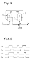
- Fig. 5 shows a block diagram of the apparatus of this embodiment.
- Fig. 6 shows an operation chart of this embodiment.
- the apparatus comprises a light source (not shown) for a predetermined value, an optical selector 121 for receiving an input data signal (I D ) at a side "0" input terminal thereof and inputting an input clock signal (I C ) at an light selection signal terminal thereof, and an optical selector 122 with no light input applied to the side "0" input terminal and a constant light input (I l ) from the light source for a predetermined value applied to a side "1" input terminal thereof.
- the output signal of the optical selector 121 is divided into two optical signals by a half-mirror 202.
- One of the divided signals is applied to the light selection signal terminal of the optical selector 122, and at the same time the other of the divided signals is the output optical signal of the apparatus.
- the output signal of the optical selector 122 is applied to the side "1" input terminal of the optical selector 121.
- the input signal applied to the side "0" input terminal that is, the input data signal is selected to be the output of the optical selector 121 and outputted to the outside of the apparatus. Further, the input data signal is also applied to the light selection signal terminal of the optical selector 122, so that the output signal of the optical selector 122 is the signal having the same logical value as the input data signal.
- the input clock signal changes from “0" to "1” the input signal applied to the side "1" input terminal, that is, the value of the input data signal just before the input clock signal changes to "1” is selected to be the output of the optical selector 121.
- This value is applied to the light selection signal terminal of the optical selector 122, so that the output of the optical selector 121 is maintained with this value and the output optical signal is also maintained with this value.
- the optical signal output is the same logical value as the input data signal as described above.
- the operation of the optical selector involves both suitable signal delay and integration of signal waveform, so that oscillation in a feedback loop can be avoided.
- An apparatus of this embodiment is what is called an edge trigger latch which holds and then outputs a logical value of an input data signal when an input clock signal rises from "0" to "1".
- Fig. 7 shows a block diagram of the apparatus of this embodiment.
- Fig. 8 shows an operation chart of this embodiment.
- the apparatus has a structure that an H-latch unit described in the above embodiment is connected with an L-latch unit also described in the above embodiment in series and either a feedback signal in the H-latch unit or a feedback signal in the L-latch unit is selected to be an output of the apparatus.
- the H-latch unit comprises a light source (not shown) for a predetermined value, an optical selector 131 for receiving an input data signal (I D ) at a a side "0" input terminal and inputting one of optical signals divided by a half-mirror 207 at an light selection signal terminal, and an optical selector 132 with no light input applied to a side "0" input terminal thereof and constant light input (I l ) from the light source for a predetermined value applied to the side "1" input terminal thereof.
- the output signal of the optical selector 131 is applied to the light selection signal terminal of the optical selector 132.
- the output signal of the optical selector 132 is divided into two optical signals by a half-mirror 203. One of signals divided by the half-mirror 203 is applied to the side "1" input terminal of the optical selector 131.
- the L-latch unit comprises a light source (not shown) for a predetermined value, an optical selector 133 for receiving one of signals divided by a half-mirror 204 at the side "1" input terminal thereof and inputting one of signals divided by a half-mirror 206 at a light selection signal terminal thereof, and an optical selector 134 with no light input applied to the side "0" input terminal and a constant light input (I l ) from the light source for a predetermined value applied to a "1" side input terminal thereof.
- the output signal of the optical selector 134 is divided into two signals by a half-mirror 205. One of the signals divided by the half-mirror 205 is applied to the light selection signal terminal of the optical selector 133, and the output signal of the optical selector 134 is applied to the side "0" input terminal of the optical selector 135.
- the other of the signals divided by the half-mirror 204 is applied to the side "1" input terminal of the optical selector 135, and the other of signals divided by the half-mirror 205 is applied to the side "0" input terminal of the optical selector 135, and the other of signals divided by the half-mirror 206 is applied to the light selection signal terminal of the optical selector 133, and then the output of the optical selector 135 is an output optical signal (I O ).
- the H-latch unit When the input clock signal is "0", the H-latch unit outputs the same logical value as the input data signal to the L-latch unit and the side "1" input terminal of the optical selector 135 at the same time. At this time, the L-latch unit outputs the signal having the logical value held therein to the side "0" input terminal of the optical selector 135.
- the optical selector 135 selects the input signal applied to the side "0" input terminal as the output, that is, the L-latch unit selects the signal having the logical value held therein as the output.
- the H-latch unit holds and then outputs the value of the input data signal right before this change.
- the L-latch unit outputs the same logical value as the output of the H-latch unit.
- the optical selector 135 selectively outputs the input signal from the H-latch unit.
- the H-latch unit outputs the signal having the same logical value as the input data signal to the L-latch unit and output to the side "1" input terminal of the optical selector 135.
- the L-latch unit holds and then outputs the output signal of the H-latch unit just before the input clock signal changes, that is, the logical value held by the H-latch unit when the input clock signal changes from "0" to "1".
- the optical selector 135 selects the input signal applied to the side "0" input terminal to be the output, that is, the L-latch unit selects a signal having the logical value held therein.
- this apparatus achieves the function of the edge trigger latch that is holding and then outputting the logical value of the input data signal when the input clock signal rises from "0" to "1".
- the operation of the optical selector involves both suitable signal delay and integration of signal waveform, so that oscillation in a feedback loop can be avoided.
- An apparatus of this embodiment is an RS flip-flop which outputs an output signal "1" when an input set signal is “1” and outputs an output signal "0" when an input reset signal is “1".
- Fig. 9 shows a block diagram of this embodiment.
- Fig. 10 shows an operation chart of this embodiment.
- This apparatus comprises a light source (not shown) for a predetermined value, an optical selector 141 for receiving an input data signal (I D ) as an optical input (I l ) at a side "1" input terminal thereof and inputting a reset signal (I R ) at an light selection signal terminal thereof, and an optical selector 142 for inputting an output signal of an optical adder 301, which add the set signal (I S ) and one of signals divided by a half-mirror 208, at a light selection signal terminal and inputting an output signal of the optical selector 141 at a side "1" input terminal with no light input applied to the side "0" input terminal.
- the output optical signal is the other of signals divided by a half-mirror 208.
- this apparatus achieves the function of the RS flip-flop which when the set signal is “1", the output is "1", and when the reset signal is “1", the output is "0" and when the set signal and reset signal are both "0", the output is the data previously held.
- the operation of the optical selector involves both suitable signal delay and integration of signal waveform, so that oscillation in a feedback loop can be avoided.
- the optical feedback circuit formation and the optical path setting for the optical logical connection is provided by edging a glass plate. In this way, a large scale circuit can be formed at the same time. Further, if a silicon substrate or a GaAs substrate is used with selecting a transmission wavelength, a current edging technic can be used, and at the same time devices to which quantum confined Stark effect or a Wannier-Stark localization effect is applied can be manufactured.
- the optical selector may comprise (1) a variable refractive index device for receiving an optical data signal and electrically changing a refractive index, (2) a refractive index controller for receiving a light selection signal carrying binary digital information, and changing a refractive index of said variable refractive index device in accordance with the value of information carried by the light selection signal, and (3) a light selection slit for transmitting only a light outputted from a specified position of said variable refractive index device, and selectively outputs a light inputted to a specified area of the variable refractive index device in accordance with a value of information carried by the light selection signal.
- the simple 1 bit latch and 1 bit flip-flop are mentioned, but combining these, a multi-bit optical digital holding device may be used.
Landscapes
- Optical Communication System (AREA)
Abstract
Description
- The present invention relates to an optical digital holding apparatus for holding instantaneous digital information borne by an optical signal.
- In opposition to a digital electronic technique represented by an electronic computer, a digital optical technique in which an electronic transmission medium is replaced from electrons to light to attain a high speed operation has been drawing the attention. In the digital optical technique, a current target is set at a digital optical computer and various methods and apparatus have been proposed and tested for an optical digital element which is a base of the configuration of the digital optical computer. One of the required optical digital devices for such an optical digital system is an optical digital holding apparatus which holds instantaneous digital information borne by an optical signal.
- Conventional optical digital holding apparatus which has been proposed and tested are as follows.
- (1) A first conventional optical digital holding device uses a method in which an intensity of an external light irradiation to the non-linear optical absorptive material in the etalon resonator is varied to control the transmittance thereof having a hysteresis characteristic.
- (2) A second conventional optical digital holding device uses a method in which a nonlinear optical absorptive region is formed in an etalon resonator of a laser diode (hereinafter called LD), and is irradiated with the light to enhance the transmittance to generate laser oscillation.
- (3) A third conventional optical digital memory device uses a method in which a light transmitted through an electro optical crystal is received and converted into electrons and this electric signal is transmitted so that it is a positive feedback to the electro optical crystal.
- (4) A forth conventional optical digital holding device uses a method in which an output light of an LED or an LD is received in a photo diode (PD), and an output electric signal of the PD is returned.
-
- It is an object of the present invention to provide an optical digital holding apparatus with simple construction, in which no bias light irradiation or complicated erase operation is required.
- An optical digital holding apparatus of the present invention carries out functions of a flip-flop apparatus (RS flip-flop, D-type flip-flop etc.) which is a kind of the electrical digital holding apparatus, and can be achieved by placing an optical connecting wiring having a direct or indirect feedback circuit which is the essence of the flip-flop circuit between the multistage optical selectors having the selector function.
- In other words, the optical digital holding apparatus of the present invention comprises (a) a set of selectors for receiving an aggregation of spatially distributed optical digital information signals propagating in a predetermined direction and bearing binary digital information and an optical control signal bearing binary digital information and selectively outputting one of a portion of an aggregation of the digital information signals which are received in accordance with a value of the digital information borne by the optical control signal, having a delay function and an integration function, placed in multistage, and (b) an optical connection wiring for connecting the selectors each other, including optical feedback connection for making an output optical signal of one of the selectors into an input optical signal of one of the other selectors and making an output optical signal of one of the other selectors into its input signal or an input signal of a selector in a stage prior to said one of the other selectors.
- Here, it is practical that the number of optical digital information signals inputting to the selection is two and the number of said optical control signal is one. At this time, aforesaid selector outputs a third optical information signal bearing the binary digital information borne by either a first optical information signal received in a first area or a second optical information signal received in a second area in accordance with the value of the binary digital information borne by the optical control information.
- It is preferred that such a selector is constructed in one of three ways hereunder in order to attain a high speed response.
- A first type of the selector comprises (1) a first variable transmittance (or reflectance) device and a second variable transmittance (or reflectance) device driven independently for controlling either the transmission (or reflection) of an input light or non-transmission (or non-reflection) of the light in accordance with an electric drive manner, (2) a first electric charge injecting device and a first electric charge discharging device, which are connected to the first variable transmittance (or reflectance) device, (3) a second electric charge injecting device and a second electric charge discharging device, which are connected to the second variable transmittance (or reflectance) device, and (4) an optical detection circuit for receiving the optical control signal, issuing an activation direction to either a first pair of the first electric charge injecting device and the second electric charge discharging device or a second pair of the second electric charge injecting device and the first electric charge discharging device, and issuing a deactivation direction to the other pairs in accordance with the value of the binary digital information carried by the optical control signal. Here, it is preferred that the variable transmittance (or reflectance) device is a self-electro-optic effect device and has either quantum confined Stark effect or Wannier-Stark localization effect.
- A second type of the selector comprises (1) a first polarization plane rotation device for selectively conducting either non-rotation or 90 degrees rotation of a polarization direction of an input linearly polarized light having a predetermined direction of polarization, (2) a double refraction plate for changing an optical path in accordance with the direction of polarization of the input linearly polarized light received through the first polarization plane rotation device, (3) a second polarization plane rotation device for selectively conduction either the non-rotation or the 90 degrees rotation of the direction of polarization of the linearly polarized light outputted from the double refraction plate, (4) a polarization plane rotation controller for setting the first polarization plane rotation device and the second polarization plane rotation device into one of a non-rotation mode and a 90 degrees rotation mode in accordance with the value of the binary digital information carried by the optical control signal, and (5) an output light selector for selecting only the light outputted from a predetermined area of the second polarization plane rotation device. Here, it is preferred that the first and second polarization plane rotation devices are twisted nematic liquid crystal cells.
- A third type of the selector comprises (1) a variable refractive index device for electrically changing a refractive index, (2) a refractive index controller for receiving the optical control signal and changing a refractive index of the variable refractive index device in accordance with the value of information carried by the optical control signal, and (3) a light selection slit for transmitting only a light outputted from a specified position of the variable refractive index device. Here, it is preferred that the variable refractive index device is made of material what is called electro optical crystal.
- In the digital optical holding apparatus, the holding function is achieved by a way such that an output optical signal of the optical selector in a preceding stage is made into an light selection signal or an input optical data signal, of the optical selector in a succeeding stage, and an output optical signal of the optical selector in the succeeding stage is made into an input optical data information or an light selection signal, of the optical selector itself in the succeeding stage or the optical selector placed in the stage prior to the selector in the succeeding stage.
- According to the optical digital holding apparatus of the present invention, the optical selectors capable of being cascade-connected are placed in multistage and optically connected each other, so that the optical digital holding apparatus itself can also be cascade-connected. Further, by combining these with another optical digital processor, a large scale optical digital apparatus such as a counter, a shift register can be achieved.
- According to the first type of the optical selector, two variable transmittance devices or variable reflectance devices having the quantum confined Stark effect or the Wannier-Stark localization effect are combined and driving transistors are prepared for the injection/discharge of the electric charges of the devices controlling the transmission/non-transmission of the light in the respective devices such that one is in the electric charge injection mode while the other is in the electric charge discharge mode in accordance with the value of information of the input optical signal carrying the selection direction information. Accordingly, the optical digital holding device which can switch the control at a high speed so that only one is exclusively controlled to the transmission state, and facilitates the cascade connection is provided.
- According to the second type of the selector, the non-rotation and the 90 degrees rotation of the direction of polarization to the input light polarized in the specific direction in the first polarization plane rotation device are controlled in accordance with the value of the information of the input signal light carrying the selection direction signal to switch the ordinary/extraordinary light of the input light in the double refraction device to change the optical path, so that the light received in the second specified area is outputted from a light selection slit for the ordinary light and the light received in the second specified area is outputted from the light selection slit for the extraordinary light. Then, the direction of polarization of the output light assured to be same as the direction of polarization of the input light by the second polarization plane rotation device. Accordingly, an optical digital holding apparatus which can select the output light at a high speed and facilitates the cascade connection is provided.
- According to the third type of the selector, since the light is selectively outputted by using the electro optical effect which reacts at a high speed to change the refractive index of the variable refractive index device, the optical digital holding apparatus which can select the output light at a high speed and facilitates the cascade connection is provided.
- The present invention will become more fully understood from the detailed description given hereinbelow and the accompanying drawings which are given by way of illustration only, and thus are not to be considered as limiting the present invention.
- Further scope of applicability of the present invention will become apparent from the detailed description given hereinafter. However, it should be understood that the detailed description and specific examples, while indicating preferred embodiments of the invention, are given by way of illustration only, since various changes and modifications within the spirit and scope of the invention will become apparent to those skilled in the art form this detailed description.
-
- Fig. 1 shows a block diagram of an optical digital holding apparatus (L latch) according to the first embodiment of this invention.
- Fig. 2 shows an operation chart in the first embodiment of this invention.
- Fig. 3 shows a block diagram of an optical selector.
- Fig. 4 shows a block diagram of an optical selector.
- Fig. 5 shows a block diagram of an optical digital holding apparatus (H latch) according to the second embodiment of this invention.
- Fig. 6 shows an operation chart in the second embodiment of this invention.
- Fig. 7 shows a block diagram of an optical digital holding apparatus (edge trigger latch) according to the third embodiment of this invention.
- Fig. 8 shows an operation chart in the third embodiment of this invention.
- Fig. 9 shows a block diagram of an optical digital holding apparatus (RS flip-flop) according to the fourth embodiment of this invention.
- Fig. 10 shows an operation chart in the fourth embodiment of this invention.
- Fig. 11 shows a block diagram of another RS flip-flop.
- Fig. 12 shows a block diagram of another RS flip-flop.
- Fig. 13 shows a block diagram of another RS flip-flop.
-
- The embodiments of this invention will be explained hereunder with reference to the accompanying drawings. In the following embodiments, the same elements are represented by the same reference numerals, and the repetitive description on the same elements is omitted. Further, all of the input/output signals of the apparatus in the following embodiments are optical signals. "0" represents absence of the optical signal, and "1" represents presence of the optical signal. In the following explanation of optical circuits, it is assumed that an optical branch unit and an light combination unit are placed in branch point of the signals and in junction of the signals respectively and a mirror or others are used for setting the optical path, which is omitted from the drawings and explanation.
- An apparatus of this embodiment is a transparency latch (hereinafter called L latch) which outputs a logical value equal to a logical value of an input data signal when an input clock signal is "1", and holds and then outputs a logical value that is the logical value of the input data signal right before the input clock signal changes from "1" to "0" when the input clock signal is "0".
- Fig. 1 shows a block diagram of the apparatus of this embodiment. Fig. 2 shows an operation chart of this embodiment. The apparatus comprises a light source (not shown) for a predetermined value, an optical selector 111 for receiving an input data signal (ID) at one of input terminals thereof to be selected as an output (hereinafter called side "1" input terminal) when an light selection signal is "1" and inputting an input clock signal (IC) at an light selection signal terminal thereof, and an
optical selector 112 with no light input applied to the side "0" input terminal and a constant light input (Il) from the light source for a predetermined value applied to one of the input terminals thereof to be selected as the output (hereinafter called side "0" input terminal) when the light selection signal is "0". The output signal of the optical selector 111 is divided into two optical signals by a half-mirror 201. One of the divided signals is applied to the light selection signal terminal of theoptical selector 112, and at the same time the other of the divided signals is the output optical signal of the apparatus. The output signal of theoptical selector 112 is applied to the side "0" input terminal of the optical selector 111. - When the input clock signal is "1", the input signal applied to the side "1" input terminal, that is, the input data signal is selected to be the output of the optical selector 111 and outputted to the outside of the apparatus. Further, the input data signal is also applied to the light selection signal terminal of the
optical selector 112, so that the output signal of theoptical selector 112 is the signal having the same logical value as the input data signal. When the input clock signal changes from "1" to "0", the input signal applied to the side "0" input terminal, that is, the value of the input data signal right before the input clock signal changes to "0" is selected to be the output of the optical selector 111. This value is applied to the light selection signal terminal of theoptical selector 112, so that the output of the optical selector 111 is maintained with this value, and the output optical signal is also maintained with this value. When the input clock signal goes to "1" again, the output optical signal is the same logical value as the input data signal as described above. - The operation of the optical selector involves both suitable signal delay and integration of signal waveform, so that oscillation in a feedback loop can be avoided.
- Fig. 3 shows the first block diagram of the optical selector for selectively outputting lights received in a specified area, which is required for constituting such an optical digital holding apparatus and can be cascade-connected. This apparatus comprises
variable transmittance devices transmittance control circuit 530 electrically connected to those devices as shown in Fig. 3. Thetransmittance control circuit 530 comprises a photo-transistor 531 for receiving an input light I,transistors - When the input light I is not applied, the
transistor 532 is conductive and thetransistor 533 is non-conductive and a voltage is applied to only thevariable transmittance device 520, which does not substantially transmit the light because an electric field is established therein. Since no electric field is established in thevariable transmittance device 510, it transmits the light at substantially full transmission. On the other hand, when the input light I is applied, thetransistor 532 is non-conductive and thetransistor 533 is conductive, so that the voltage is applied to only thevariable transmittance device 510 which does not substantially transmit the light because an electric field is established therein. Since no electric field is established in thevariable transmittance device 520, substantially all lights are transmitted therethrough. In this manner, the optical digital selector which can be cascade-connected and selectively outputs the light received in the specified area is constructed. In switching the light receiving area of the light to be transmitted, thetransistor 532 is provided for thevariable transmittance device 510 and thetransistor 533 is provided for thevariable transmittance device 520 for discharging the electric charges accumulated in the device to which the voltage has been applied before switching. Accordingly, high speed switching of the transmittance is attained. While the variable transmittance device is used in the present apparatus, a variable reflectance device may be used. - Fig. 4 shows the second block diagram of the optical selector. This apparatus comprises the first polarization
plane rotation device 610 made of 90 degrees TN liquid crystal, adouble refraction device 620 made of calcite for receiving the light outputted from the first polarizationplane rotation device 610, the second polarizationplane rotation device 630 made of 90 degrees TN liquid crystal for receiving the light outputted from thedouble refraction device 620, a light selection slit 640 for transmitting a portion of the light outputted from the second polarizationplane rotation device 630, and adeflection controller 650 for controlling the first and second polarizationplane rotation devices - In this apparatus, it is assumed that linearly polarized lights A and B are applied. When the
deflection controller 650 does not receive the input light I, thedeflection controller 650 is in the ON state so that the first and second polarizationplane rotation devices double refraction device 620 without the change in the polarization plane so that an ordinary light is applied to thedouble refraction device 620 and it goes straight and passes through thedouble refraction device 620. As a result, only the light B among the lights transmitted through the second polarization plane rotation device passes through the light selection slit and it is outputted as shown. - When the
deflection controller 650 receives the input light I, thedeflection controller 650 is in the OFF state and the first and second polarizationplane rotation devices double refraction device 620 with the polarization plane changed, they are extraordinary rays to thedouble refraction device 620 with the modified optical path. As a result, only the light A among the lights transmitted through the second polarization plane rotation device and having the polarization direction thereof returned to the original direction passes through the light selection slit and it is outputted as shown. - It is noted that the optical selectors with the above-described construction are used in the following embodiments.
- An apparatus of this embodiment is a transparency latch (hereinafter called H latch) which outputs a logical value equal to a logical value of an input data signal when an input clock signal is "0", and holds and then outputs a logical value that is the logical value of the input data signal right before the input clock signal changes from "0" to "1" when the input clock signal is "1".
- Fig. 5 shows a block diagram of the apparatus of this embodiment. Fig. 6 shows an operation chart of this embodiment. The apparatus comprises a light source (not shown) for a predetermined value, an
optical selector 121 for receiving an input data signal (ID) at a side "0" input terminal thereof and inputting an input clock signal (IC) at an light selection signal terminal thereof, and anoptical selector 122 with no light input applied to the side "0" input terminal and a constant light input (Il) from the light source for a predetermined value applied to a side "1" input terminal thereof. The output signal of theoptical selector 121 is divided into two optical signals by a half-mirror 202. One of the divided signals is applied to the light selection signal terminal of theoptical selector 122, and at the same time the other of the divided signals is the output optical signal of the apparatus. The output signal of theoptical selector 122 is applied to the side "1" input terminal of theoptical selector 121. - When the input clock signal is "0", the input signal applied to the side "0" input terminal, that is, the input data signal is selected to be the output of the
optical selector 121 and outputted to the outside of the apparatus. Further, the input data signal is also applied to the light selection signal terminal of theoptical selector 122, so that the output signal of theoptical selector 122 is the signal having the same logical value as the input data signal. When the input clock signal changes from "0" to "1", the input signal applied to the side "1" input terminal, that is, the value of the input data signal just before the input clock signal changes to "1" is selected to be the output of theoptical selector 121. This value is applied to the light selection signal terminal of theoptical selector 122, so that the output of theoptical selector 121 is maintained with this value and the output optical signal is also maintained with this value. When the input clock signal goes to "0" again, the optical signal output is the same logical value as the input data signal as described above. - Similar to the first embodiment, the operation of the optical selector involves both suitable signal delay and integration of signal waveform, so that oscillation in a feedback loop can be avoided.
- An apparatus of this embodiment is what is called an edge trigger latch which holds and then outputs a logical value of an input data signal when an input clock signal rises from "0" to "1".
- Fig. 7 shows a block diagram of the apparatus of this embodiment. Fig. 8 shows an operation chart of this embodiment. The apparatus has a structure that an H-latch unit described in the above embodiment is connected with an L-latch unit also described in the above embodiment in series and either a feedback signal in the H-latch unit or a feedback signal in the L-latch unit is selected to be an output of the apparatus.
- The H-latch unit comprises a light source (not shown) for a predetermined value, an
optical selector 131 for receiving an input data signal (ID) at a a side "0" input terminal and inputting one of optical signals divided by a half-mirror 207 at an light selection signal terminal, and anoptical selector 132 with no light input applied to a side "0" input terminal thereof and constant light input (Il) from the light source for a predetermined value applied to the side "1" input terminal thereof. The output signal of theoptical selector 131 is applied to the light selection signal terminal of theoptical selector 132. The output signal of theoptical selector 132 is divided into two optical signals by a half-mirror 203. One of signals divided by the half-mirror 203 is applied to the side "1" input terminal of theoptical selector 131. - The L-latch unit comprises a light source (not shown) for a predetermined value, an
optical selector 133 for receiving one of signals divided by a half-mirror 204 at the side "1" input terminal thereof and inputting one of signals divided by a half-mirror 206 at a light selection signal terminal thereof, and anoptical selector 134 with no light input applied to the side "0" input terminal and a constant light input (Il) from the light source for a predetermined value applied to a "1" side input terminal thereof. The output signal of theoptical selector 134 is divided into two signals by a half-mirror 205. One of the signals divided by the half-mirror 205 is applied to the light selection signal terminal of theoptical selector 133, and the output signal of theoptical selector 134 is applied to the side "0" input terminal of theoptical selector 135. - Further, the other of the signals divided by the half-
mirror 204 is applied to the side "1" input terminal of theoptical selector 135, and the other of signals divided by the half-mirror 205 is applied to the side "0" input terminal of theoptical selector 135, and the other of signals divided by the half-mirror 206 is applied to the light selection signal terminal of theoptical selector 133, and then the output of theoptical selector 135 is an output optical signal (IO). - When the input clock signal is "0", the H-latch unit outputs the same logical value as the input data signal to the L-latch unit and the side "1" input terminal of the
optical selector 135 at the same time. At this time, the L-latch unit outputs the signal having the logical value held therein to the side "0" input terminal of theoptical selector 135. Theoptical selector 135 selects the input signal applied to the side "0" input terminal as the output, that is, the L-latch unit selects the signal having the logical value held therein as the output. - Next, when the input clock signal changes from "0" to "1", the H-latch unit holds and then outputs the value of the input data signal right before this change. The L-latch unit outputs the same logical value as the output of the H-latch unit. As a result, the
optical selector 135 selectively outputs the input signal from the H-latch unit. - Next, when the input clock signal changes from "1" to "0", the H-latch unit outputs the signal having the same logical value as the input data signal to the L-latch unit and output to the side "1" input terminal of the
optical selector 135. The L-latch unit holds and then outputs the output signal of the H-latch unit just before the input clock signal changes, that is, the logical value held by the H-latch unit when the input clock signal changes from "0" to "1". Theoptical selector 135 selects the input signal applied to the side "0" input terminal to be the output, that is, the L-latch unit selects a signal having the logical value held therein. - Accordingly, this apparatus achieves the function of the edge trigger latch that is holding and then outputting the logical value of the input data signal when the input clock signal rises from "0" to "1".
- Similar to the first embodiment, the operation of the optical selector involves both suitable signal delay and integration of signal waveform, so that oscillation in a feedback loop can be avoided.
- An apparatus of this embodiment is an RS flip-flop which outputs an output signal "1" when an input set signal is "1" and outputs an output signal "0" when an input reset signal is "1".
- Fig. 9 shows a block diagram of this embodiment. Fig. 10 shows an operation chart of this embodiment. This apparatus comprises a light source (not shown) for a predetermined value, an
optical selector 141 for receiving an input data signal (ID) as an optical input (Il) at a side "1" input terminal thereof and inputting a reset signal (IR) at an light selection signal terminal thereof, and anoptical selector 142 for inputting an output signal of anoptical adder 301, which add the set signal (IS) and one of signals divided by a half-mirror 208, at a light selection signal terminal and inputting an output signal of theoptical selector 141 at a side "1" input terminal with no light input applied to the side "0" input terminal. The output optical signal is the other of signals divided by a half-mirror 208. - As the set signal becomes "1" while the reset signal has been "0", the output of the
optical selector 141 is "1" and the output optical signal is always "1". As a result, the input to the light selection signal terminal of theoptical selector 142 becomes "1". - Next, as the reset signal becomes "1" while the reset signal has been "0", the output of the
optical selector 141 is "0" and the input to the light selection signal terminal of theselector 142 is "0", so that the output optical signal becomes "0" and the input to the light selection signal terminal of theoptical selector 142 is maintained with "0". - Accordingly, this apparatus achieves the function of the RS flip-flop which when the set signal is "1", the output is "1", and when the reset signal is "1", the output is "0" and when the set signal and reset signal are both "0", the output is the data previously held.
- Similar to the first embodiment, the operation of the optical selector involves both suitable signal delay and integration of signal waveform, so that oscillation in a feedback loop can be avoided.
- Further, even the optical circuit is constructed as shown in Fig. 11 - Fig. 13, the RS flip-flop which can operate in the same manner as the embodiments is obtained.
- The optical feedback circuit formation and the optical path setting for the optical logical connection is provided by edging a glass plate. In this way, a large scale circuit can be formed at the same time. Further, if a silicon substrate or a GaAs substrate is used with selecting a transmission wavelength, a current edging technic can be used, and at the same time devices to which quantum confined Stark effect or a Wannier-Stark localization effect is applied can be manufactured.
- The present invention is not limited to the embodiments as described above but various modification thereof may be made. For example, the optical selector may comprise (1) a variable refractive index device for receiving an optical data signal and electrically changing a refractive index, (2) a refractive index controller for receiving a light selection signal carrying binary digital information, and changing a refractive index of said variable refractive index device in accordance with the value of information carried by the light selection signal, and (3) a light selection slit for transmitting only a light outputted from a specified position of said variable refractive index device, and selectively outputs a light inputted to a specified area of the variable refractive index device in accordance with a value of information carried by the light selection signal. Further, in the embodiments, the simple 1 bit latch and 1 bit flip-flop are mentioned, but combining these, a multi-bit optical digital holding device may be used.
- From the invention thus described, it will be obvious that the invention may be varied in many ways. Such variations are not to be regarded as a departure from the spirit and scope of the invention, and all such modifications as would be obvious to one skilled in the art are intended to be included within the scope of the following claims.
Claims (9)
- An optical storing unit for storing digital data, the storing unit comprising two optical elements (141, 142) each havingsignal inputs for receiving one or more input optical signals (I1, A);a control input for receiving a control signal (IR, IS);transfer characteristics controllable by the control signal (IR, IS) ; andan output for outputting an optical signal (IO) depending on the one or more input optical signals (I1, A,) and the control signal (IR, IS);in which optical storing unit the optical elements (141, 142) are connected to receive an optical data signal (I1) and a control signal (IR, IS) defining time periods, and are connected together so that the optical signal (IO) at the output of one element is fed back to a control input of that one element and thereby causes data carried by the optical data signal (I1) to be stored in the unit during a time period defined by the control signal (IR, IS).
- An optical storing unit as claimed in claim 1, wherein a first one of the two optical elements (141) has a signal input (0) connected to receive said optical data signal (I1) and a control input connected to receive a reset signal (IR), and a second one of the two optical elements (142) has a signal input (1) connected to receive the signal (A) output from the first optical element (141) and a control input connected to receive a signal representing a set signal (IS) added to the signal (IO) output from the second optical element (142).
- An optical storing unit as claimed in claim 1 or 2, wherein the two optical elements together comprise first and second variable light devices (510, 520) each having voltage-dependent light properties, the storing unit further comprising a phototransistor (531) for receiving the control signal (IR, IS) and two transistors (532, 533) both connected to the phototransistor (531) to be controlled thereby so that when one transistor (532, 533) is turned on by the phototransistor the other transistor (532, 533) is turned off, and each connected to a respective one of the light devices (510, 520) for such control thereby that the light properties of one device (510, 520) is the logical inverse of that of the other device (510, 520).
- An optical storing unit as claimed in claim 3, wherein the first and second variable light devices (510, 520) are light transmittance devices each having voltage-dependent light transmitting properties.
- An optical storing unit as claimed in claim 3, where the first and second variable light devices (510, 520) are light reflectance devices each having voltage-dependant light reflecting properties.
- An optical storing unit as claimed in any of claims 3 to 5, wherein each variable light device (510, 520) is a self-electro-optic effect device and has either quantum confined Stark effect or Wannier-Stark localization effect.
- An optical storing unit as claimed in claim 1 or 2, wherein said elements comprise:a first polarization plane rotation device (610) for selectively conducting either non-rotation or 90 degrees rotation of a polarization direction of an input signal of linearly polarized light having a predetermined direction of polarization;a double refraction plate (620) for changing an optical path in accordance with the polarization direction in the input linearly polarized light received through said first polarization plane rotation device;a second polarization plane rotation device (630) for selectively conducting either the non-rotation or the 90 degrees rotation of the polarization direction in the linearly polarized light outputted from said double refraction plate;a polarization plane rotation controller (650) for setting said first polarization plane rotation device and said second polarization plane rotation device into either a non-rotation mode or a 90 degrees rotation mode in accordance with a value of the binary digital information borne by the optical control signal; andan output light selector (640) for selecting only the light outputted from a predetermined area of said second polarization plane rotation device.
- An optical storing unit according to claim 7, wherein said first (610) and second (620) polarization plane rotation devices include twisted nematic liquid crystal cells.
- An optical storing unit apparatus according to claim 1 or 2, wherein said elements comprise:a variable refractive index device for electrically changing a refractive index;a refractive index controller for receiving said optical control signal and changing a refractive index of said variable refractive index device in accordance with a value of information carried by the optical control signal; anda light selection slit for transmitting only a light outputted from a specified position of said variable refractive index device;and wherein said selector selectively outputs an optical digital information signal inputted to a specified area of said variable refractive index device in accordance with a value of information carried by said optical control signal.
Applications Claiming Priority (3)
| Application Number | Priority Date | Filing Date | Title |
|---|---|---|---|
| JP6868793 | 1993-03-26 | ||
| JP5068687A JPH06281987A (en) | 1993-03-26 | 1993-03-26 | Optical digital storage |
| EP94302174A EP0617511A3 (en) | 1993-03-26 | 1994-03-25 | Optical digital holding apparatus. |
Related Parent Applications (1)
| Application Number | Title | Priority Date | Filing Date |
|---|---|---|---|
| EP94302174A Division EP0617511A3 (en) | 1993-03-26 | 1994-03-25 | Optical digital holding apparatus. |
Publications (1)
| Publication Number | Publication Date |
|---|---|
| EP0933872A1 true EP0933872A1 (en) | 1999-08-04 |
Family
ID=13380911
Family Applications (2)
| Application Number | Title | Priority Date | Filing Date |
|---|---|---|---|
| EP94302174A Withdrawn EP0617511A3 (en) | 1993-03-26 | 1994-03-25 | Optical digital holding apparatus. |
| EP99107155A Ceased EP0933872A1 (en) | 1993-03-26 | 1994-03-25 | Optical digital holding apparatus |
Family Applications Before (1)
| Application Number | Title | Priority Date | Filing Date |
|---|---|---|---|
| EP94302174A Withdrawn EP0617511A3 (en) | 1993-03-26 | 1994-03-25 | Optical digital holding apparatus. |
Country Status (3)
| Country | Link |
|---|---|
| US (1) | US5617232A (en) |
| EP (2) | EP0617511A3 (en) |
| JP (1) | JPH06281987A (en) |
Families Citing this family (10)
| Publication number | Priority date | Publication date | Assignee | Title |
|---|---|---|---|---|
| US5999284A (en) * | 1997-06-05 | 1999-12-07 | Northern Telecom Limited | Optical detection and logic devices with latching function |
| EP1035428A3 (en) * | 1999-03-02 | 2005-07-27 | Fuji Photo Film Co., Ltd. | Optical logic device and optical memory device |
| US7518796B2 (en) * | 2001-02-09 | 2009-04-14 | Nortel Networks Limited | Optical device having nonmonotonic transfer function and applications using same |
| US6516106B2 (en) | 2001-02-09 | 2003-02-04 | Nortel Networks Limited | Subtracting analog noise from an optical communication channel using stable, non-absorbing optical hard limiters |
| US6693732B2 (en) | 2001-02-09 | 2004-02-17 | Nortel Networks Limited | Optical sampler based on stable, non-absorbing optical hard limiters |
| US6674559B2 (en) | 2001-02-09 | 2004-01-06 | Nortel Networks Limited | Optical automatic gain control based on stable, non-absorbing optical hard limiters |
| US6636337B2 (en) | 2001-02-09 | 2003-10-21 | Nortel Networks Limited | Optical switching device based on stable, non-absorbing optical hard limiters |
| US20020154350A1 (en) * | 2001-02-09 | 2002-10-24 | Johnson Erik V. | Optical logic devices based on stable, non-absorbing optical hard limiters |
| US7110154B2 (en) | 2004-06-10 | 2006-09-19 | Clemson University | Plasmon-photon coupled optical devices |
| KR102239084B1 (en) * | 2019-09-26 | 2021-04-12 | 인하대학교 산학협력단 | Analog-digital interface sram based on optoelectronic devices |
Citations (5)
| Publication number | Priority date | Publication date | Assignee | Title |
|---|---|---|---|---|
| JPS6064521A (en) * | 1983-09-19 | 1985-04-13 | Matsushita Electric Ind Co Ltd | Optical flip-flop circuit |
| US4761060A (en) * | 1984-11-07 | 1988-08-02 | Nec Corporation | Optical delay type flipflop and shift register using it |
| US4802175A (en) * | 1983-09-06 | 1989-01-31 | Nec Corporation | Opto-electric logic elements |
| US4900115A (en) * | 1989-01-31 | 1990-02-13 | University Of Colorado Foundation, Inc. | Optical logic circuit useful for bit serial optic computing |
| EP0517441A1 (en) * | 1991-06-06 | 1992-12-09 | AT&T Corp. | Dynamic optical logic |
Family Cites Families (14)
| Publication number | Priority date | Publication date | Assignee | Title |
|---|---|---|---|---|
| JPS5889887A (en) * | 1981-11-25 | 1983-05-28 | Univ Tohoku | Semiconductor optical function device |
| US4675518A (en) * | 1982-03-05 | 1987-06-23 | Omron Tateisi Electronics Co. | Optical bistable device |
| JPS59223015A (en) * | 1983-06-02 | 1984-12-14 | Nec Corp | Optical jk flip-flop circuit |
| JPH01245231A (en) * | 1988-03-28 | 1989-09-29 | Nippon Hoso Kyokai <Nhk> | Parallel optical logic computing element |
| SU1603334A1 (en) * | 1988-04-20 | 1990-10-30 | Винницкий политехнический институт | Optical device for logical processing of images |
| JP2653468B2 (en) * | 1988-05-16 | 1997-09-17 | 日本電信電話株式会社 | Optical parallel processing method and apparatus |
| JPH0220037A (en) * | 1988-07-07 | 1990-01-23 | Matsushita Electron Corp | Inspecting method for semiconductor device |
| JPH0297922A (en) * | 1988-10-04 | 1990-04-10 | Nec Corp | Light flip-flop |
| JPH02230224A (en) * | 1989-03-03 | 1990-09-12 | Nippon Telegr & Teleph Corp <Ntt> | Optical flip-flop |
| US4978842A (en) * | 1989-04-21 | 1990-12-18 | At&T Bell Laboratories | Programmable optical logic device with complementary inputs |
| US4964687A (en) * | 1989-09-29 | 1990-10-23 | The Boeing Company | Optical latch and method of latching data using same |
| US5528702A (en) * | 1991-05-31 | 1996-06-18 | Seiko Instruments Inc. | Optical pattern recognition apparatus with coordinate conversion function |
| JP2855985B2 (en) * | 1992-08-19 | 1999-02-10 | 三菱自動車工業株式会社 | Anti-skid brake device |
| JPH06148710A (en) * | 1992-09-18 | 1994-05-27 | Hamamatsu Photonics Kk | Optical digital device |
-
1993
- 1993-03-26 JP JP5068687A patent/JPH06281987A/en active Pending
-
1994
- 1994-03-25 EP EP94302174A patent/EP0617511A3/en not_active Withdrawn
- 1994-03-25 US US08/217,652 patent/US5617232A/en not_active Expired - Fee Related
- 1994-03-25 EP EP99107155A patent/EP0933872A1/en not_active Ceased
Patent Citations (5)
| Publication number | Priority date | Publication date | Assignee | Title |
|---|---|---|---|---|
| US4802175A (en) * | 1983-09-06 | 1989-01-31 | Nec Corporation | Opto-electric logic elements |
| JPS6064521A (en) * | 1983-09-19 | 1985-04-13 | Matsushita Electric Ind Co Ltd | Optical flip-flop circuit |
| US4761060A (en) * | 1984-11-07 | 1988-08-02 | Nec Corporation | Optical delay type flipflop and shift register using it |
| US4900115A (en) * | 1989-01-31 | 1990-02-13 | University Of Colorado Foundation, Inc. | Optical logic circuit useful for bit serial optic computing |
| EP0517441A1 (en) * | 1991-06-06 | 1992-12-09 | AT&T Corp. | Dynamic optical logic |
Non-Patent Citations (1)
| Title |
|---|
| PATENT ABSTRACTS OF JAPAN vol. 009, no. 197 (E - 335) 14 August 1985 (1985-08-14) * |
Also Published As
| Publication number | Publication date |
|---|---|
| US5617232A (en) | 1997-04-01 |
| JPH06281987A (en) | 1994-10-07 |
| EP0617511A2 (en) | 1994-09-28 |
| EP0617511A3 (en) | 1995-11-29 |
Similar Documents
| Publication | Publication Date | Title |
|---|---|---|
| US4754132A (en) | Symmetric optical device with quantum well absorption | |
| US5617232A (en) | Optical digital holding apparatus | |
| WO1988008554A1 (en) | Optical device | |
| US4115706A (en) | Integrated circuit having one-input terminal with selectively varying input levels | |
| EP0376483B1 (en) | Monolithic apparatus comprising optically interconnected quantum well devices | |
| US4967068A (en) | Single-ended optical logic arrangement | |
| US4577189A (en) | Circuits with electro-optical feedback for display and a digitizer application | |
| EP0364162B1 (en) | Optical device | |
| US5345455A (en) | Optical wavelength converter control method and device | |
| US5185831A (en) | Optical waveguide device | |
| EP0415617A2 (en) | Differential optical logic arrangement | |
| EP0224542A1 (en) | Optical logic device and assembly. | |
| JPH04280522A (en) | Optical connector and its drive method | |
| US3427456A (en) | Laser images formed by matric control | |
| US4802175A (en) | Opto-electric logic elements | |
| JPS60254991A (en) | Time-division optical exchange | |
| US5442471A (en) | Optical digital apparatus | |
| USH1296H (en) | Optical switching device and parallel processing architecture | |
| US3093477A (en) | Electro-optical bistable light switch | |
| MacGillivray et al. | Photonic Logic | |
| WO1988006828A1 (en) | Signal switching processor | |
| Ichikawa et al. | An all optical programmable logic gate | |
| JPH0439837B2 (en) | ||
| JPH0413120A (en) | Optical bistable flip-flop device | |
| Delville et al. | Optical hysteresis, memory, and avalanche events in laser-induced liquid-liquid phase separation |
Legal Events
| Date | Code | Title | Description |
|---|---|---|---|
| PUAI | Public reference made under article 153(3) epc to a published international application that has entered the european phase |
Free format text: ORIGINAL CODE: 0009012 |
|
| AC | Divisional application: reference to earlier application |
Ref document number: 617511 Country of ref document: EP |
|
| AK | Designated contracting states |
Kind code of ref document: A1 Designated state(s): DE FR GB |
|
| RIC1 | Information provided on ipc code assigned before grant |
Free format text: 6H 03K 3/42 A, 6G 02F 3/02 B |
|
| 17P | Request for examination filed |
Effective date: 20000112 |
|
| 17Q | First examination report despatched |
Effective date: 20000925 |
|
| GRAG | Despatch of communication of intention to grant |
Free format text: ORIGINAL CODE: EPIDOS AGRA |
|
| STAA | Information on the status of an ep patent application or granted ep patent |
Free format text: STATUS: THE APPLICATION HAS BEEN REFUSED |
|
| 18R | Application refused |
Effective date: 20011110 |