EP0933660A1 - Optical transmitting-receiving waveguide module - Google Patents
Optical transmitting-receiving waveguide module Download PDFInfo
- Publication number
- EP0933660A1 EP0933660A1 EP99101326A EP99101326A EP0933660A1 EP 0933660 A1 EP0933660 A1 EP 0933660A1 EP 99101326 A EP99101326 A EP 99101326A EP 99101326 A EP99101326 A EP 99101326A EP 0933660 A1 EP0933660 A1 EP 0933660A1
- Authority
- EP
- European Patent Office
- Prior art keywords
- light
- receiving
- waveguide
- emitting element
- optical transmitting
- Prior art date
- Legal status (The legal status is an assumption and is not a legal conclusion. Google has not performed a legal analysis and makes no representation as to the accuracy of the status listed.)
- Withdrawn
Links
Images


Classifications
-
- G—PHYSICS
- G02—OPTICS
- G02B—OPTICAL ELEMENTS, SYSTEMS OR APPARATUS
- G02B6/00—Light guides; Structural details of arrangements comprising light guides and other optical elements, e.g. couplings
- G02B6/24—Coupling light guides
- G02B6/42—Coupling light guides with opto-electronic elements
- G02B6/4201—Packages, e.g. shape, construction, internal or external details
- G02B6/4246—Bidirectionally operating package structures
Definitions
- This invention relates to an optical transmitting-receiving waveguide module that is applicable to the bidirectional communications, and more particularly to, an optical transmitting-receiving waveguide module with a built-in transmission-monitoring light-receiving element.
- FIG.1 is a perspective view showing parts related with this invention in prior arts 1 and 2.
- 101 is a waveguide substrate
- 102 is a light-emitting element (e.g., a laser diode) installed on the waveguide substrate 101
- 108 is a transmission-monitoring light-receiving element (e.g., a photodiode) installed on the waveguide substrate 101
- 109 is a receiving light-receiving element (e.g., a photodiode) installed on the waveguide substrate 101
- 104 is first part of waveguide formed on the waveguide substrate 101
- 105 is a Y-branch of the waveguide
- 106 is second part of the waveguide
- 107 is third part of the waveguide.
- the end face of the first part 104 is optically connected with an optical fiber (not shown), and the light-emitting element 102 and the light-receiving elements 108, 109 each are provided with an electrode.
- Light emitted from the light-emitting element 102 is sent through the waveguides 106, 105 and 104 to the optical fiber, and light from the optical fiber passes through the waveguides 104, 105 and 107 and then is converted into an electrical signal by the receiving light-receiving element 109.
- Light emitted from the back face of the light-emitting element 102 is received by the transmission-monitoring light-receiving element 108, used for the transmission monitoring.
- the retails of the structure and operation of the module shown in FIG.1 are described in prior arts 1 and 2, and therefore its explanations are omitted herein.
- the light-emitting element 102, light-receiving elements 108, 109, waveguides 104, 105, 106 and 107 are all of core-layer structure, and the core layer is continuously formed in the propagation direction of light.
- the position arrangement of the respective elements in plan view is as shown in FIG.1.
- the conventional modules in prior arts 1 and 2 have problems described below. Namely, since the receiving light-receiving element 109 and the transmission-monitoring light-receiving element 108 are installed lying side by side, such a sufficient interval between the two elements as to allow the installation is necessary. Therefore, the modules are hard to miniaturize.
- the light-emitting element 102 In installing the three elements, the light-emitting element 102, receiving light-receiving element 109 and transmission-monitoring light-receiving element 108, it is necessary to provide three kinds of solders, whose fusion temperatures are different from one another. Namely, severe precision is required for the installation of optical element, and therefore it must be avoided that solder at already-installed element is softened due to the heat conduction in heating solder at second-or-later-installed element.
- an object of the invention to provide an optical transmitting-receiving waveguide module that is miniaturized and can provide reduced cost in manufacturing.
- an optical transmitting-receiving waveguide module comprising:
- FIG.2 is a cross sectional view showing the first preferred embodiment of the invention. Meanwhile, in the drawings referred below, same or like parts are indicated by same reference numerals and bring out like operations, therefore its duplicated explanations will be omitted.
- 1 is an optical waveguide substrate
- 2 is a light-emitting element installed on the waveguide substrate 1
- 3 is combined light-receiving elements, where a transmission-monitoring light-receiving element 8 and a receiving light-receiving element 9 are formed integrally.
- 10 is an optical fiber
- 11 is a package
- 12 is a V-groove formed on the waveguide substrate 1 by which the axis of the optical fiber 10 is fixed.
- the optical fiber 10 is installed positioned by the V-groove 12 without requiring its optical axis adjustment.
- the light-emitting element 2 is installed so as to connect with the second part 6 of the waveguide, and is desirably a spot size conversion type light-emitting element which allows the connection loss to be reduced.
- the combined light-receiving elements 3 are so installed that the transmission-monitoring light-receiving element 8 can connect with light emitted from the back face of the light-emitting element 2.
- FIG.3 is an enlarged perspective view showing the installation state of the light-emitting element 2 and the combined light-receiving elements 3 in FIG.2.
- Used in the example shown in FIG.3 is an end face incidence type light-receiving element that can provide the simple structure to optically connect with the end face of the third part 7 of the waveguide.
- a waveguide incidence type light-receiving element that can provide the simple structure may be used.
- Transmission signal light emitted from the front end face of the light-emitting element 2 is connected through the waveguides 6, 5 and 4 to the optical fiber 10, and is thereby sent to a transmission line.
- Light emitted from the back face of the light-receiving element 2 is supplied to the transmission-monitoring light-receiving element 8, where the optical output of the light-receiving element 2 is monitored.
- Reception signal light sent through the transmission line is supplied from the optical fiber 10 through the waveguides 4, 5 and 7 to the receiving light-receiving element 9, converted into an electrical signal.
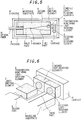
- FIG.4 is a perspective view showing the second preferred embodiment of the invention, where only part corresponding to FIG.3 in the module is shown. The other part is like that of the first embodiment in FIG.2.
- both the transmission-monitoring light-receiving element 8 and the receiving light-receiving element 9 employ a surface incidence type light-receiving element.
- numeral 13 is a reflecting mirror.
- the reflecting mirror 13 is composed such that light emitted from the end face of the third part 7 of the waveguide is reflected by the reflecting mirror 13, supplied to the surface incidence type light-receiving element 9, and such that light emitted from the back face of the light-emitting element 2 is reflected by the reflecting mirror 13, supplied to the surface incidence type light-receiving element 8.
- FIG.5 is a cross sectional view showing the third preferred embodiment of the invention.
- 14 is a carriage on which the combined light-receiving elements are mounted.
- FIG.6 is an enlarged perspective view showing the light-emitting element 2 and the combined light-receiving elements 3 in FIG.5.
- the combined light-receiving elements 3 are mounted not on the waveguide substrate 1 but on the separately-provided carriage 14 by solder bonding etc. Directing the light-receiving face of the combined light-receiving elements to the waveguide substrate 1, the carriage 14 is positioned such that light emitted from the end face of the third part 7 of the waveguide is received by the light-receiving face of the receiving light-receiving element 9 and such that light emitted from the back face of the light-emitting element 2 is received by the light-receiving face of the transmission-monitoring light-receiving element 8.
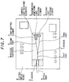
- FIG.7 is a partial cross sectional and plan view showing the fourth preferred embodiment of the invention.
- 15 is an electric circuit board.
- the optical transmitting-receiving waveguide module may be installed on the electric circuit board 15, instead of being contained in the package 11.
- the first advantage of the invention is that the optical transmitting-receiving waveguide module can be sufficiently miniaturized. This is because the interval between the transmission-monitoring light-receiving element 8 and the receiving light-receiving element 9 is minimized by using the combined light-receiving elements 3, therefore, the interval between the light-emitting element 2 and the receiving light-receiving element 9 can be minimized, thereby shortening the Y-branch of the waveguide as minimum as possible.
- the second advantage of the invention is that the installation cost of light-receiving element in the manufacturing process of the optical transmitting-receiving waveguide module can be reduced. This is because, whereas, in the conventional modules, two of the transmission-monitoring light-receiving element and the receiving light-receiving element have been installed, one body of the combined light-receiving elements only has to be installed in this invention.
Landscapes
- Physics & Mathematics (AREA)
- General Physics & Mathematics (AREA)
- Optics & Photonics (AREA)
- Optical Integrated Circuits (AREA)
- Optical Communication System (AREA)
- Optical Couplings Of Light Guides (AREA)
Abstract
The optical waveguide transceiver module consists of a Y-branch
optical waveguide (5) connected to an optical fiber (10) fixed in a
v-groove (12), one branch (6) of the optical waveguide connected to a
light emitting element (2) and the second branch (7) connected to a
receiving light receiving element (9). The receiving photodiode (9) is
formed integrally with a transmission monitoring light receiving element
(8) which receives the emission from the back face of the light emitting
element (2). The use of a combined light receiving element (3) reduces
the size of the module. Preferably the light emitting element (2) is of
the spot-size conversion type. In one embodiment a reflecting mirror
(13) is used to reflect the light from the back face of the light
emitting element (2) and the signal from the second branch (7) onto
surface incidence type combined light receiving elements (3).
Description
- This invention relates to an optical transmitting-receiving waveguide module that is applicable to the bidirectional communications, and more particularly to, an optical transmitting-receiving waveguide module with a built-in transmission-monitoring light-receiving element.
- Conventional optical transmitting-receiving waveguide modules are, for example, described in 1997 IEICE Electronics Society Meeting C-3-6 (hereinafter referred to as 'prior art 1') and in Japanese patent application laid-open No.9-191152(1997) (hereinafter referred to as 'prior art 2').
- FIG.1 is a perspective view showing parts related with this invention in
prior arts waveguide substrate waveguide substrate waveguide substrate waveguide substrate - The end face of the
first part 104 is optically connected with an optical fiber (not shown), and the light-emitting element 102 and the light-receivingelements - Light emitted from the light-emitting
element 102 is sent through thewaveguides waveguides element 109. Light emitted from the back face of the light-emittingelement 102 is received by the transmission-monitoring light-receivingelement 108, used for the transmission monitoring. - The retails of the structure and operation of the module shown in FIG.1 are described in
prior arts prior art 2, the light-emittingelement 102, light-receiving elements waveguides - The conventional modules in
prior arts element 109 and the transmission-monitoring light-receivingelement 108 are installed lying side by side, such a sufficient interval between the two elements as to allow the installation is necessary. Therefore, the modules are hard to miniaturize. - Also, the number of process in the installation is increased, and therefore the manufacturing cost is difficult to reduce.
- Further, in installing the three elements, the light-emitting
element 102, receiving light-receivingelement 109 and transmission-monitoring light-receivingelement 108, it is necessary to provide three kinds of solders, whose fusion temperatures are different from one another. Namely, severe precision is required for the installation of optical element, and therefore it must be avoided that solder at already-installed element is softened due to the heat conduction in heating solder at second-or-later-installed element. - Meanwhile, this problem does not occur in the module disclosed in
prior art 2 since both the light-emitting element and the light-receiving element are formed as the core-layer structure. - Accordingly, it is an object of the invention to provide an optical transmitting-receiving waveguide module that is miniaturized and can provide reduced cost in manufacturing.
- According to the invention, an optical transmitting-receiving waveguide module, comprising:
- a groove which is formed on a waveguide substrate so as to fix the beginning end of an optical fiber;
- first part of waveguide which is formed on the waveguide substrate so as to connect with an end face of the optical fiber in the waveguide substrate;
- a Y-branch of waveguide to branch the first part of waveguide into second part of waveguide and third part of waveguide which are formed on the waveguide substrate;
- a light-emitting element installed on the waveguide substrate; and
- combined light-receiving elements that a receiving light-receiving
element and a transmission-monitoring light-receiving
element are integrally formed, the transmission-monitoring
light-receiving element of the combined light-receiving elements
being installed at a position to connect with light emitted from the
back face of the light-emitting element;
wherein the second part of waveguide extending from the Y-branch of waveguide has an end face positioned to connect with light emitted from the light-emitting surface of the light-emitting element, and the third part of waveguide extending from the Y-branch of waveguide has an end face positioned to connect with the light-receiving surface of the receiving light-receiving element of the combined light-receiving elements. -
- The invention will be explained in more detail in conjunction with the appended drawings, wherein:
- FIG.1 is a perspective view showing the conventional optical transmitting-receiving waveguide module,
- FIG.2 is a cross sectional view showing an optical transmitting-receiving waveguide module in a first preferred embodiment according to the invention,
- FIG.3 is an enlarged perspective view showing a light-emitting element and combined light-receiving elements in FIG.2,
- FIG.4 is a partial perspective view showing an optical transmitting-receiving waveguide module in a second preferred embodiment according to the invention,
- FIG.5 is a cross sectional view showing an optical transmitting-receiving waveguide module in a third preferred embodiment according to the invention,
- FIG.6 is an enlarged perspective view showing a light-emitting element and combined light-receiving elements in FIG.5, and
- FIG.7 is a partial cross sectional and plan view showing an optical transmitting-receiving waveguide module in a fourth preferred embodiment according to the invention.
-
- The preferred embodiments of this invention will be explained below, referring to the drawings.
- FIG.2 is a cross sectional view showing the first preferred embodiment of the invention. Meanwhile, in the drawings referred below, same or like parts are indicated by same reference numerals and bring out like operations, therefore its duplicated explanations will be omitted.
- In FIG.2, 1 is an optical waveguide substrate, 2 is a light-emitting element installed on the
waveguide substrate element 8 and a receiving light-receivingelement 9 are formed integrally. On thewaveguide substrate 1, there is formed a waveguide, where 4 is first part of the waveguide, 5 is a Y-branch of the waveguide, 6 is second part of the waveguide and 7 is third part of the waveguide. - 10 is an optical fiber, 11 is a package and 12 is a V-groove formed on the
waveguide substrate 1 by which the axis of theoptical fiber 10 is fixed. - The
optical fiber 10 is installed positioned by the V-groove 12 without requiring its optical axis adjustment. The light-emittingelement 2 is installed so as to connect with thesecond part 6 of the waveguide, and is desirably a spot size conversion type light-emitting element which allows the connection loss to be reduced. The combined light-receivingelements 3 are so installed that the transmission-monitoring light-receivingelement 8 can connect with light emitted from the back face of the light-emittingelement 2. - FIG.3 is an enlarged perspective view showing the installation state of the light-emitting
element 2 and the combined light-receivingelements 3 in FIG.2. Used in the example shown in FIG.3 is an end face incidence type light-receiving element that can provide the simple structure to optically connect with the end face of thethird part 7 of the waveguide. Alternatively, a waveguide incidence type light-receiving element that can provide the simple structure may be used. - Transmission signal light emitted from the front end face of the light-emitting
element 2 is connected through thewaveguides optical fiber 10, and is thereby sent to a transmission line. Light emitted from the back face of the light-receivingelement 2 is supplied to the transmission-monitoring light-receivingelement 8, where the optical output of the light-receivingelement 2 is monitored. - Reception signal light sent through the transmission line is supplied from the
optical fiber 10 through thewaveguides element 9, converted into an electrical signal. - FIG.4 is a perspective view showing the second preferred embodiment of the invention, where only part corresponding to FIG.3 in the module is shown. The other part is like that of the first embodiment in FIG.2.
- In this embodiment shown in FIG.4, both the transmission-monitoring light-receiving
element 8 and the receiving light-receivingelement 9 employ a surface incidence type light-receiving element. Also, in FIG.4,numeral 13 is a reflecting mirror. The reflectingmirror 13 is composed such that light emitted from the end face of thethird part 7 of the waveguide is reflected by the reflectingmirror 13, supplied to the surface incidence type light-receivingelement 9, and such that light emitted from the back face of the light-emittingelement 2 is reflected by the reflectingmirror 13, supplied to the surface incidence type light-receivingelement 8. - FIG.5 is a cross sectional view showing the third preferred embodiment of the invention. 14 is a carriage on which the combined light-receiving elements are mounted. FIG.6 is an enlarged perspective view showing the light-emitting
element 2 and the combined light-receivingelements 3 in FIG.5. - In this embodiment, the combined light-receiving
elements 3 are mounted not on thewaveguide substrate 1 but on the separately-providedcarriage 14 by solder bonding etc. Directing the light-receiving face of the combined light-receiving elements to thewaveguide substrate 1, thecarriage 14 is positioned such that light emitted from the end face of thethird part 7 of the waveguide is received by the light-receiving face of the receiving light-receivingelement 9 and such that light emitted from the back face of the light-emittingelement 2 is received by the light-receiving face of the transmission-monitoring light-receivingelement 8. - FIG.7 is a partial cross sectional and plan view showing the fourth preferred embodiment of the invention. 15 is an electric circuit board. The optical transmitting-receiving waveguide module may be installed on the
electric circuit board 15, instead of being contained in thepackage 11. - The first advantage of the invention is that the optical transmitting-receiving waveguide module can be sufficiently miniaturized. This is because the interval between the transmission-monitoring light-receiving
element 8 and the receiving light-receivingelement 9 is minimized by using the combined light-receivingelements 3, therefore, the interval between the light-emittingelement 2 and the receiving light-receivingelement 9 can be minimized, thereby shortening the Y-branch of the waveguide as minimum as possible. - The second advantage of the invention is that the installation cost of light-receiving element in the manufacturing process of the optical transmitting-receiving waveguide module can be reduced. This is because, whereas, in the conventional modules, two of the transmission-monitoring light-receiving element and the receiving light-receiving element have been installed, one body of the combined light-receiving elements only has to be installed in this invention.
- Although the invention has been described with respect to specific embodiment for complete and clear disclosure, the appended claims are not to be thus limited but are to be construed as embodying all modification and alternative constructions that may be occurred to one skilled in the art which fairly fall within the basic teaching here is set forth.
Claims (7)
- An optical transmitting-receiving waveguide module, comprising:a groove which is formed on a waveguide substrate so as to fix the beginning end of an optical fiber;first part of waveguide which is formed on said waveguide substrate so as to connect with an end face of said optical fiber in said waveguide substrate;a Y-branch of waveguide to branch said first part of waveguide into second part of waveguide and third part of waveguide which are formed on said waveguide substrate;a light-emitting element installed on said waveguide substrate; andcombined light-receiving elements that a receiving light-receiving element and a transmission-monitoring light-receiving element are integrally formed, said transmission-monitoring light-receiving element of said combined light-receiving elements being installed at a position to connect with light emitted from the back face of said light-emitting element;
wherein said second part of waveguide extending from said Y-branch of waveguide has an end face positioned to connect with light emitted from the light-emitting surface of said light-emitting element, and said third part of waveguide extending from said Y-branch of waveguide has an end face positioned to connect with the light-receiving surface of said receiving light-receiving element of said combined light-receiving elements. - An optical transmitting-receiving waveguide module, according to claim 1, wherein:said light-emitting element is a spot size conversion type light-emitting element.
- An optical transmitting-receiving waveguide module, according to claim 1, wherein:said combined light-receiving elements are a waveguide incidence type light-receiving element or a end face incidence type light-receiving element.
- An optical transmitting-receiving waveguide module, according to claim 1, wherein:said combined light-receiving elements are a surface incidence type light-receiving element, and said waveguide substrate is provided with a reflecting mirror installed such that light emitted from the end face of said third part of waveguide is reflected by said reflecting mirror and then supplied to said surface incidence type receiving light-receiving element and such that light emitted from the back face of said light-emitting element is reflected by said reflecting mirror and then supplied to said surface incidence type transmission-monitoring light-receiving element.
- An optical transmitting-receiving waveguide module, according to claim 1, further comprising:a carriage to surmount said combined light-receiving elements.
- An optical transmitting-receiving waveguide module, according to claim 1, further comprising:a package to contain said optical transmitting-receiving waveguide module.
- An optical transmitting-receiving waveguide module, according to claim 1, further comprising:an electric circuit board to surmount said optical transmitting-receiving waveguide module.
Applications Claiming Priority (2)
| Application Number | Priority Date | Filing Date | Title |
|---|---|---|---|
| JP3230798 | 1998-01-30 | ||
| JP10032307A JP3065015B2 (en) | 1998-01-30 | 1998-01-30 | Optical transmission / reception waveguide module |
Publications (1)
| Publication Number | Publication Date |
|---|---|
| EP0933660A1 true EP0933660A1 (en) | 1999-08-04 |
Family
ID=12355296
Family Applications (1)
| Application Number | Title | Priority Date | Filing Date |
|---|---|---|---|
| EP99101326A Withdrawn EP0933660A1 (en) | 1998-01-30 | 1999-01-25 | Optical transmitting-receiving waveguide module |
Country Status (2)
| Country | Link |
|---|---|
| EP (1) | EP0933660A1 (en) |
| JP (1) | JP3065015B2 (en) |
Cited By (1)
| Publication number | Priority date | Publication date | Assignee | Title |
|---|---|---|---|---|
| EP1296169A2 (en) * | 2001-09-21 | 2003-03-26 | Citizen Electronics Co., Ltd. | Bidirectional optical transmission device |
Families Citing this family (2)
| Publication number | Priority date | Publication date | Assignee | Title |
|---|---|---|---|---|
| JP3902394B2 (en) | 2000-10-23 | 2007-04-04 | 日本電気株式会社 | Optical communication module and optical communication device |
| JP7384091B2 (en) * | 2020-03-26 | 2023-11-21 | Tdk株式会社 | Integrated optical device, integrated optical module, and method for manufacturing integrated optical device |
Citations (3)
| Publication number | Priority date | Publication date | Assignee | Title |
|---|---|---|---|---|
| JPH04328704A (en) * | 1991-04-30 | 1992-11-17 | Oki Electric Ind Co Ltd | Optical transmission and reception module |
| EP0660146A1 (en) * | 1993-12-27 | 1995-06-28 | Nec Corporation | Light-receiving structure for waveguide type optical devices |
| JPH10133066A (en) * | 1996-10-29 | 1998-05-22 | Kyocera Corp | Optical waveguide type module |
-
1998
- 1998-01-30 JP JP10032307A patent/JP3065015B2/en not_active Expired - Fee Related
-
1999
- 1999-01-25 EP EP99101326A patent/EP0933660A1/en not_active Withdrawn
Patent Citations (3)
| Publication number | Priority date | Publication date | Assignee | Title |
|---|---|---|---|---|
| JPH04328704A (en) * | 1991-04-30 | 1992-11-17 | Oki Electric Ind Co Ltd | Optical transmission and reception module |
| EP0660146A1 (en) * | 1993-12-27 | 1995-06-28 | Nec Corporation | Light-receiving structure for waveguide type optical devices |
| JPH10133066A (en) * | 1996-10-29 | 1998-05-22 | Kyocera Corp | Optical waveguide type module |
Non-Patent Citations (4)
| Title |
|---|
| NAKAGAWA G ET AL: "HIGH POWER AND HIGH SENSITIVITY PLANAR LIGHTWAVE CIRCUIT MODULE INCORPORATING A NOVEL PASSIVE ALIGNMENT METHOD", JOURNAL OF LIGHTWAVE TECHNOLOGY, vol. 16, no. 1, January 1998 (1998-01-01), pages 66 - 71, XP000739110 * |
| PATENT ABSTRACTS OF JAPAN vol. 017, no. 166 (P - 1514) 30 March 1993 (1993-03-30) * |
| PATENT ABSTRACTS OF JAPAN vol. 098, no. 010 31 August 1998 (1998-08-31) * |
| UCHIDA N ET AL: "LOW-COST HYBRID WDM MODULE CONSISTING OF A SPOT-SIZE CONVERTER INTEGRATED LASER DIODE AND A WAVEGUIDE PHOTODIODE ON A PLC PLATFORMFOR ACCESS NETWORK SYSTEMS", IEICE TRANSACTIONS ON ELECTRONICS, vol. E80-C, no. 1, January 1997 (1997-01-01), pages 88 - 97, XP000740609 * |
Cited By (2)
| Publication number | Priority date | Publication date | Assignee | Title |
|---|---|---|---|---|
| EP1296169A2 (en) * | 2001-09-21 | 2003-03-26 | Citizen Electronics Co., Ltd. | Bidirectional optical transmission device |
| EP1296169A3 (en) * | 2001-09-21 | 2003-05-21 | Citizen Electronics Co., Ltd. | Bidirectional optical transmission device |
Also Published As
| Publication number | Publication date |
|---|---|
| JPH11218629A (en) | 1999-08-10 |
| JP3065015B2 (en) | 2000-07-12 |
Similar Documents
| Publication | Publication Date | Title |
|---|---|---|
| EP1160599B1 (en) | Semiconductor laser diode module | |
| US5499309A (en) | Method of fabricating optical component including first and second optical waveguide chips having opposed inclined surfaces | |
| EP0654689B1 (en) | Optical module for two-way transmission | |
| US6250820B1 (en) | Electrooptical coupling component | |
| US5497438A (en) | Optical transmission and reception module having coupled optical waveguide chips | |
| EP0782023B1 (en) | Optical transmitter-receiver module | |
| JP2000171671A (en) | Optical communication module and its mounting method | |
| US6408121B1 (en) | Optical communication module | |
| JPH10173207A (en) | Optical transmission-reception module | |
| US6402394B1 (en) | Optical transmitting/receiving module | |
| US20050158054A1 (en) | Optical module for bi-directional communication system | |
| US6478479B1 (en) | Optical connector module with optical fibers for connecting optical module and optical fiber connector | |
| EP0933660A1 (en) | Optical transmitting-receiving waveguide module | |
| US7099536B1 (en) | Single lens system integrating both transmissive and reflective surfaces for light focusing to an optical fiber and light reflection back to a monitor photodetector | |
| JP3767842B2 (en) | Bi-directional optical communication module | |
| JP2003519823A (en) | Optical coupling system | |
| CA2359002A1 (en) | Optoelectric module for multi-fiber arrays | |
| US6312167B1 (en) | Light transmission module | |
| EP1233487B1 (en) | Optical semiconductor module equipped with a light monitor for monitoring signal light emitted from a light emitting element | |
| JPH07209556A (en) | Optical transmission and reception module | |
| JP3295327B2 (en) | Bidirectional optical module | |
| JP2006084890A (en) | Optical connection device | |
| JP2000009953A (en) | Wavelength demultiplexer and optical transmission and reception module having the demultiplexer | |
| JPH05297250A (en) | Optical semiconductor module | |
| JPH04309908A (en) | Wavelength multiplex transmission and reception module |
Legal Events
| Date | Code | Title | Description |
|---|---|---|---|
| PUAI | Public reference made under article 153(3) epc to a published international application that has entered the european phase |
Free format text: ORIGINAL CODE: 0009012 |
|
| 17P | Request for examination filed |
Effective date: 19990526 |
|
| AK | Designated contracting states |
Kind code of ref document: A1 Designated state(s): DE FR GB IT |
|
| AX | Request for extension of the european patent |
Free format text: AL;LT;LV;MK;RO;SI |
|
| AKX | Designation fees paid |
Free format text: DE FR GB IT |
|
| STAA | Information on the status of an ep patent application or granted ep patent |
Free format text: STATUS: THE APPLICATION HAS BEEN WITHDRAWN |
|
| 18W | Application withdrawn |
Withdrawal date: 20020726 |