EP0932146A2 - Optical pickup and method of adjusting same - Google Patents
Optical pickup and method of adjusting same Download PDFInfo
- Publication number
- EP0932146A2 EP0932146A2 EP99101265A EP99101265A EP0932146A2 EP 0932146 A2 EP0932146 A2 EP 0932146A2 EP 99101265 A EP99101265 A EP 99101265A EP 99101265 A EP99101265 A EP 99101265A EP 0932146 A2 EP0932146 A2 EP 0932146A2
- Authority
- EP
- European Patent Office
- Prior art keywords
- waveform
- light receiving
- receiving elements
- region
- lens
- Prior art date
- Legal status (The legal status is an assumption and is not a legal conclusion. Google has not performed a legal analysis and makes no representation as to the accuracy of the status listed.)
- Granted
Links
- 230000003287 optical effect Effects 0.000 title claims abstract description 30
- 238000000034 method Methods 0.000 title claims description 14
- 239000004065 semiconductor Substances 0.000 description 8
- 230000001419 dependent effect Effects 0.000 description 2
- 239000000758 substrate Substances 0.000 description 2
- VYPSYNLAJGMNEJ-UHFFFAOYSA-N Silicium dioxide Chemical compound O=[Si]=O VYPSYNLAJGMNEJ-UHFFFAOYSA-N 0.000 description 1
- 238000010586 diagram Methods 0.000 description 1
- 238000006073 displacement reaction Methods 0.000 description 1
- 230000010287 polarization Effects 0.000 description 1
- 230000005855 radiation Effects 0.000 description 1
- 239000011347 resin Substances 0.000 description 1
- 229920005989 resin Polymers 0.000 description 1
Images




Classifications
-
- G—PHYSICS
- G11—INFORMATION STORAGE
- G11B—INFORMATION STORAGE BASED ON RELATIVE MOVEMENT BETWEEN RECORD CARRIER AND TRANSDUCER
- G11B7/00—Recording or reproducing by optical means, e.g. recording using a thermal beam of optical radiation by modifying optical properties or the physical structure, reproducing using an optical beam at lower power by sensing optical properties; Record carriers therefor
- G11B7/12—Heads, e.g. forming of the optical beam spot or modulation of the optical beam
- G11B7/135—Means for guiding the beam from the source to the record carrier or from the record carrier to the detector
- G11B7/1353—Diffractive elements, e.g. holograms or gratings
-
- G—PHYSICS
- G11—INFORMATION STORAGE
- G11B—INFORMATION STORAGE BASED ON RELATIVE MOVEMENT BETWEEN RECORD CARRIER AND TRANSDUCER
- G11B7/00—Recording or reproducing by optical means, e.g. recording using a thermal beam of optical radiation by modifying optical properties or the physical structure, reproducing using an optical beam at lower power by sensing optical properties; Record carriers therefor
- G11B7/12—Heads, e.g. forming of the optical beam spot or modulation of the optical beam
- G11B7/13—Optical detectors therefor
- G11B7/131—Arrangement of detectors in a multiple array
-
- G—PHYSICS
- G11—INFORMATION STORAGE
- G11B—INFORMATION STORAGE BASED ON RELATIVE MOVEMENT BETWEEN RECORD CARRIER AND TRANSDUCER
- G11B7/00—Recording or reproducing by optical means, e.g. recording using a thermal beam of optical radiation by modifying optical properties or the physical structure, reproducing using an optical beam at lower power by sensing optical properties; Record carriers therefor
- G11B7/12—Heads, e.g. forming of the optical beam spot or modulation of the optical beam
- G11B7/22—Apparatus or processes for the manufacture of optical heads, e.g. assembly
-
- G—PHYSICS
- G11—INFORMATION STORAGE
- G11B—INFORMATION STORAGE BASED ON RELATIVE MOVEMENT BETWEEN RECORD CARRIER AND TRANSDUCER
- G11B7/00—Recording or reproducing by optical means, e.g. recording using a thermal beam of optical radiation by modifying optical properties or the physical structure, reproducing using an optical beam at lower power by sensing optical properties; Record carriers therefor
- G11B7/08—Disposition or mounting of heads or light sources relatively to record carriers
- G11B7/09—Disposition or mounting of heads or light sources relatively to record carriers with provision for moving the light beam or focus plane for the purpose of maintaining alignment of the light beam relative to the record carrier during transducing operation, e.g. to compensate for surface irregularities of the latter or for track following
- G11B7/0943—Methods and circuits for performing mathematical operations on individual detector segment outputs
Definitions
- the present invention relates to optical pickups, and more particularly to an optical pickup and method of adjusting same used to read information from an optical disc (hereinafter merely referred to as "disc"), such as CD and DVD.
- disc an optical disc
- the adjustment in positional relationship between the diffraction element 3 and the light receiving element 7 requires actual rotation of the disc 6 to perform focusing servo using a servo circuit.
- the diffraction element 3 is displaced such that the jitter value observed by a jitter meter is brought to a best.
- This invention is characterized by a method of adjusting an optical pickup having a laser device for emitting laser light, a lens for converging the laser light on a disc, a diffraction element divided into two of a first region and a second region to respectively cause diffraction in reflected light from the disc, and a photo-detector separated by a divisional line extending almost in a same direction as a direction of diffraction by the first region and including a first portion and a second portion onto which the reflected light diffracted by the first region converges and a third portion onto which the reflection light diffracted by the second region converges, the adjusting method comprising the steps of: placing a mirror in a position of the disc; grasping as a waveform a relationship between a position of the lens and respective output values of the first portion and the second portion; and displacing the diffraction element such that the waveform becomes a predetermined state.
- the third portion may be divided, for example, as a portion 3a and a portion 3b, in order to grasp as waveforms 3a and 3b a relationship between the change in lens position and respective outputs of the portions 3a and 3b.
- the diffraction element m,ay be displaced such that the intersection of the first and second waveforms is brought into overlap with the intersection of the waveform 3a and the waveform 3b, i.e., such that the spot size assumes a minimum. Due to this, the focusing offset can be prevented with the jitter value taken best.
- the number of output signals increases due to the division of the third portion into the portions 3a and 3b.
- two signals can be selectively taken out through one terminal by a switch means. This can prevent the number of terminals from increasing.
- An optical pickup to be favorably utilized in the adjusting method of the present invention comprises: a lens for converging a laser beam from a laser device on a disc; a diffraction element divided into two of first and second regions for diffracting a reflection beam from the disc; four light receiving elements on which first and second reflection light respectively diffracted by the first and second regions converge; and a switch means for switching over between four output signals individually taken from the for light receiving elements and three output signals taken out by adding together two of four output signals.
- Another optical pickup comprises: a first diffraction element for causing a laser beam from a laser device to be split into one main beam and two sub-beams; a lens for converging the main beam and the sub-beams on a disc; a second diffraction element divided into two of first and second regions to respectively cause diffraction in the reflection beams from the disc; a photo-detector having four light emitting elements to converge thereon reflection beams of the main beam respectively diffracted by the first region and the second region, and two light receiving elements for converging thereon reflection beams of the sub-beams; and a switching means for switching over between taking out an output signal associated with any of the four light receiving elements and taking out a tracking error signal by subtracting between output signals of the two light receiving elements.
- the positional relationship between the diffraction element and the photo-detector is easy to adjust. Also, there is no neccesity of separately providing a servo circuit or the like, thus reducing cost. Meanwhile, Because the jitter value can be determined best as a result that the spot size is brought into a minimum at a point where focusing servo is effected, the optical pickup is stabilized in characteristic. Moreover, the number of terminals is prevented from increasing, thereby preventing against increase in package size.
- An optical pickup 10 of the present embodiment is to read information out of an optical disc (hereinafter merely "disc") 14, such as CD and DVD, being rotated by a disc motor 12, and includes a semiconductor laser device 16 as a light source to emit a predetermined wavelength of laser light.
- a hologram unit 18 as a diffraction element and an objective lens 20 are arranged between the semiconductor laser device 16 and the disc 14.
- a photo-detector 22 is provided obliquely below the hologram unit 18. Note that these semiconductor laser device 16, hologram unit 18 and photo-detector 22 are formed in one body as a unit 24 as shown in Figure 4.
- the hologram unit 18 includes a substrate 26 made of a quartz glass or the like.
- the substrate 26 has a grating pattern 28 formed at an underside surface in order to create three beams, and a hologram pattern 30 on a top surface to cause polarization of light.
- the hologram pattern 30 is divided with a first region 30a and a second region 30b by a divisional line A0 extending in a diametrical direction of the disc 14, as shown in Figure 3.
- the regions 30a and 30b are provided with respective gratings different in period.
- the hologram unit 18 is held by a support member 32 ( Figure 1) which is to be displaced in directions X, Y and ⁇ by a servo motor.
- the objective lens 20 is fixed to an actuator coil 34 constituting a focusing actuator so that it is vertically displaced by energizing the actuator coil 34.
- the photo-detector 22 is divided into five portions, i.e., light receiving elements 22a, 22b, 22c, 22e and 24f.
- the light receiving element 22a and the light receiving element 22b are separated by a divisional line B0 is given almost in a same direction as but slightly deviated from a direction of diffraction by the hologram pattern 30 in order to prevent against focusing offset.
- a computer 36 is connected to the support member 32, the actuator coil 34 and the light receiving elements 22a - 22f of the photo-detector 22.
- the computer 36 is connected with an APC (Automatic Power Control) 38 to control the output of the semiconductor laser device 16.
- APC Automatic Power Control
- an adjusting method is employed to conduct adjustment on the positional relationship between the hologram unit 18 and the photo-detector 22 as shown in Figure 4, in order to prevent against focusing offset and bring best the jitter value.
- step 1 ⁇ first prepared is a stem 24a having a semiconductor laser device 16 and a photo-detector 22 incorporated therein in one body.
- a UV resin 40 is applied to a top surface of the stem 24a.
- step 2 ⁇ the semiconductor laser device 16 is caused to emit light, to thereby determine its light emission center with using a CCD camera 42.
- step 3 ⁇ a hologram unit 18 is recognized by the CCD camera 42 to determine its device center.
- step 4 ⁇ the hologram unit 18 is mounted on the top surface of the stem 24a.
- this hologram unit 18 is fixed at a predetermined position as shown in Figure 1.
- a half mirror (or total reflection mirror) 46 in place of a disc 14, is placed on the turntable 44 to be rotated by the disc motor 12, and the semiconductor laser device 16 is caused to emit light.
- the laser beam from the semiconductor laser device 16 is diffracted by the grating pattern 28, and split into 0-order diffraction light (main beam) and two of 1-order diffraction light (sub-beams).
- the three beams thus split by the grating pattern 28 travels through the hologram pattern 30, and then converged on the half mirror 46 through the objective lens 20.
- the reflection light of the main beam from the half mirror 46 travels through the objective lens 20, being diffracted by the hologram pattern 30.
- the light diffracted by the region 30a shown in Figure 3 is converged onto the light receiving elements 22a and 22b of the photo-detector 22, while the light diffracted by the region 30b is onto the light receiving element 22c.
- the actuator coil 34 is energized to move the objective lens 20 in vertical directions.
- a graph as shown in Figure 5 is grasped by the computer 36 as to a relationship between a vertical position of the objective lens 20, i.e., a position perpendicular to the record surface of the disc 14 (voltage on the actuator coil 34) and output values from the light receiving elements 22a, 22b and 22c of the photo-detector 22.
- spots 1 - 9 are shown in Figure 3 corresponding to lens positions 1 - 9 in Figure 5.
- a point P represents an intersection of between an output waveform A given from the light receiving element 22a and an output waveform B from the light receiving element 22b, i.e., the point toward which focusing servo is effected.
- a point Q represents a center point in a maximum value range (the range the output assumes its maximum) of an output waveform C given from the light receiving element 22c.
- the point Q can be determined as an intersection of the output waveform C with a vertical line L2 as shown in Figure 6, wherein a horizontal line L1 is drawn through a point lower by 0.3 V than a peak value of the output waveform C and a horizontal line L2 is then drawn to equally divide into two an area S (the area hatched in Figure 6) above the horizontal line L1.
- This point Q represents a point at which the size of a laser spot assumes its minimum. Accordingly, if the intersection P and the point Q are in overlap with each other, focus servo is effected at that point with a minimum spot size. As a result, the jitter value becomes best.
- a not-shown servo motor is controlled by the computer 36 to move the support member 32 so that the hologram unit 18 is aligned in position to bring the intersection P overlap with the point Q.
- Figure 3 shows a state wherein there exists a deviation in angle ⁇ between the hologram unit 18 and the photo-detector 22.
- the hologram unit 18 is rotated by an angle ⁇ in an arrow direction from the state of Figure 3, the point P and the point Q become overlapping with each other.
- the hologram unit 18 is optimally determined of position by repeating several times such positional adjustment of the hologram unit 18 as described above.
- step 6 ⁇ light radiation is made to a contact area between the stem 24a and the hologram unit 18, thus fixing the hologram unit 18.
- This embodiment can lower cost because of no necessity of separately providing a servo circuit and the like to enable positional adjustment. Furthermore, the jitter value can be obtained best as a result of minimizing the spot size at a point to which focus servo is effected. It is therefore possible for the optical pickup 10 to stabilize the characteristic.
- the hologram unit 18 was aligned in position so as to bring the intersection P of the output waveforms A and B into overlapping with the point Q.
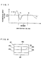
- the hologram unit 18 may be aligned in position in a manner overlapping a zero cross point (the point to which focus servo is effected) P1 of an S waveform (A - B) with a point Q as shown in Figure 7, so that the difference in output value between the light receiving elements 22a and 22b can be grasped as an S waveform (A - B) by the computer 36.
- the above-described embodiment employed the photo-detector 22 having five divided portions (light receiving elements).
- a photo-detector 48 as shown in Figures 8 and 9 may be used which is divided into six portions (light receiving elements).
- the photo-detector 48 includes six light receiving elements 48a, 48b, 48c1, 48c2, 48e, 48f.
- the light receiving elements 48a - 48f are connected with corresponding amplifiers 50a - 50f.
- the amplifiers 50a and 50b have output signals respectively given onto terminals 52a and 52b.
- the amplifiers 50c1 and 50c2 have output signals which are added together by an adder 54 and then given onto a terminal 52c.
- the output signals of the amplifiers 50c1 and 50c2 are respectively given onto terminals 52d and 52e, when the switches 56a and 56b are in a first state.
- the amplifiers 50e and 50f have output signals which are respectively given onto terminals 52d and 52e, when switches 56a and 56b are in a second state.
- the switches 56a and 56b are operated based on an output signal of a voltage comparator circuit 58 that is dependent upon a reference voltage applied to a terminal 52f.
- the hologram unit 18 is adjusted in position such that an intersection P1 (the point to which focus servo is effected) of between an output wave A of the light receiving element 48a taken out through the terminal 52a and an output waveform B of the light receiving element 48b taken through the terminal 52b is brought into overlap with an intersection P2 (the point at which the laser spot size assumes a minimum) of between an output waveform C1 of the light receiving element 48c1 - through the terminal 52d and an output waveform c2 of the light receiving element 48c2 - through the terminal 52e.
- intersection P1 the point to which focus servo is effected
- the switches 56a and 56b are put in the second state. Subtraction is made between an output signals of the light receiving element 50e taken through the terminal 52d and an output signal of the light receiving element 50f taken through the terminal 52e to thereby obtain a tracking error signal. The output signals through the terminals 52a, 52b and 52c are added together to thereby obtain a pit signal.
- the hologram unit 18 becomes easy to adjust of position depending on increased number of signals. Furthermore, because two or more signals can be selectively obtained by switching the switches 56a and 56b, it is possible to prevent against increase in the number of terminals and in package size.
- a photo-detector 60 as shown in Figure 11 may be used in place of the above-described photo-detector 22 ( Figure 2) or photo-detector 48 ( Figure 8, Figure 9).
- This photo-detector 60 includes six light receiving elements 60a, 60b, 60c1, 60c2, 60e, 60f.
- the light receiving elements 60a - 60f are connected with corresponding amplifiers 62a - 62f.
- the amplifiers 62a, 62b, 62c1 and 62c2 have output signals which are added together by an adder 64 and then taken as a pit signal Rf through a terminal 66a.
- the amplifiers 62a and 62b have output signals which are subjected to subtraction by a subtracter 68 and when taken through a terminal 66b. Also, the amplifiers 60e and 60f have output signals which are respectively taken through terminals 66c and 66d.
- the amplifiers 62c1 and 62c2 have output signals which are subjected to subtraction by a subtracter 72 when the switch 70e in the first state, while the amplifiers 62e and 62f have output signals which are subjected to subtraction by a subtracter 74 and taken through a terminal 66e when the switch 70 is in the second state.
- the switch 70 is operated based on an output signal of a voltage comparator circuit 76 that is dependent upon a reference voltage applied to a terminal 66f.
- the objective lens 20 may be vertically moved with the switch 70 placed in the first state.
- the hologram unit 18 may be adjusted in position such that a zero cross point (the point to which focussing servo is effected) P1 in an S waveform (A - B) taken through the terminal 66b is overlapped with zero cross point (the point at which the laser spot size assumes a minimum) P2 in an S waveform C1 - C2) taken through the terminal 66e.
- the switch 70 is put in the second state to obtain a tracking error signal TE through the terminal 66e and a pit signal RF through the terminal 66a.
- the hologram unit 18 can be easily adjusted in position without increasing the number of terminals in a manner similar to the case using the photo-detector 48.
- the above-described photo-detectors 48 ( Figure 8 and Figure 9) and 60 ( Figure 11) are one examples of a photo-detector having six light receiving element.
- the adders 54 and 64 and the subtracters 68, 72 and 74 may be arbitrarily combined to take other signals from the terminals.
Landscapes
- Physics & Mathematics (AREA)
- Optics & Photonics (AREA)
- Optical Head (AREA)
- Optical Recording Or Reproduction (AREA)
Abstract
Description
Claims (11)
- A method of adjusting an optical pickup having a laser device for emitting laser light, a lens for converging the laser light on a disc, a diffraction element divided into two of a first region and a second region to respectively cause diffraction in reflected light from said disc, and a photo-detector separated by a divisional line extending almost in a same direction as a direction of diffraction by said first region and including a first portion and a second portion onto which the reflected light diffracted by said first region converges and a third portion onto which the reflection light diffracted by said second region converges, said adjusting method comprising the steps of:placing a mirror in a position of said disc;grasping as a waveform a relationship between a position of said lens and respective output values of said first portion and said second portion; anddisplacing said diffraction element such that the waveform becomes a predetermined state.
- An adjusting method according to claim 1, wherein the relationship between the position of said lens and the respective output values of said first portion and said second portion is grasped as first and second waveforms, a relationship between the position of said lens and an output value of said third portion being grasped as a third waveform, and said diffraction element being displaced such that an intersection of the first waveform and the second waveform is brought into overlap with a center point of a maximum value range of the third waveform.
- An adjusting method according to claim 1, wherein a relationship between the position of said lens and a difference in output value between said first portion and said second portion is grasped as an S waveform, a relationship between the position of said lens and an output value of said third portion being grasped as a third waveform, and said diffraction element being displaced such that a zero cross point of the S waveform is brought into overlap with a center point of maximum value range of the third waveform.
- An adjusting method according to claim 1, wherein said third portion includes portions 3a and 3b separated by a divisional line extending almost in a same direction as a direction of diffraction by said second region to respectively converge the reflection light diffracted by said second region thereon, a relationship between the position of said lens and respective output values of said portions 3a and 3b being grasped as waveforms 3a and 3b, and said diffraction element being displaced such that an intersection of the first waveform and the second waveform is brought into overlap with an intersection of the waveform 3a and the waveform 3b.
- An adjusting method according to claim 1, wherein said third portion includes portions 3a and 3b separated by a divisional line extending almost in a same direction as a direction of diffraction by said second region to converge the reflection beam diffracted by said second region thereon, a relationship between the position of said lens and a difference in output value between said first portion and said second portion being grasped as a 1S waveform, a relationship between a positional change of said lens and a difference in output value between said portions 3a and 3b being grasped as a 2S waveform, and said diffraction element being displaced such that a zero cross point of the 1S waveform is brought into overlap with a zero cross point of the said 2S waveform.
- An optical pickup comprising:a lens for converging a laser beam from a laser device on a disc;a diffraction element divided into two of first and second regions for diffracting a reflection beam from said disc;four light receiving elements on which first and second reflection light respectively diffracted by said first and second regions converge; and a switch means for switching over between four output signals individually taken from said for light receiving elements and three output signals taken out by adding together two of four output signals.
- An optical pickup according to claim 6, further comprising an adder to output a bit signal by totaling the four output signals from said four light receiving elements.
- An optical pickup according to claim 6 or 7, further comprising a subtracter to determine a difference in output signal from two light receiving elements of said four light receiving elements.
- An optical pickup comprising:a first diffraction element for causing a laser beam from a laser device to be split into one main beam and two sub-beams;a lens for converging the main beam and the sub-beams on a disc;a second diffraction element divided into two of first and second regions to respectively cause diffraction in the reflection beams from said disc;a photo-detector having four light emitting elements to converge thereon reflection beams of the main beam respectively diffracted by said first region and said second region, and two light receiving elements for converging thereon reflection beams of the sub-beams; anda switching means for switching over between taking out an output signal associated with any of said four light receiving elements and taking out a tracking error signal by subtracting between output signals of said two light receiving elements.
- An optical pickup according to claim 9, further comprising an adder to output a pit signal by totaling for output signals from said four light receiving elements.
- An optical pickup according to claim 9 or 10, further comprising a subtracter to determine a difference in output signal from two light receiving elements of said four light receiving elements.
Priority Applications (1)
| Application Number | Priority Date | Filing Date | Title |
|---|---|---|---|
| EP06006046A EP1667135B1 (en) | 1998-01-23 | 1999-01-22 | Method of adjusting an optical pickup |
Applications Claiming Priority (2)
| Application Number | Priority Date | Filing Date | Title |
|---|---|---|---|
| JP10011356A JPH11213441A (en) | 1998-01-23 | 1998-01-23 | Optical pickup and its adjusting method |
| JP1135698 | 1998-01-23 |
Related Child Applications (1)
| Application Number | Title | Priority Date | Filing Date |
|---|---|---|---|
| EP06006046A Division EP1667135B1 (en) | 1998-01-23 | 1999-01-22 | Method of adjusting an optical pickup |
Publications (3)
| Publication Number | Publication Date |
|---|---|
| EP0932146A2 true EP0932146A2 (en) | 1999-07-28 |
| EP0932146A3 EP0932146A3 (en) | 1999-12-08 |
| EP0932146B1 EP0932146B1 (en) | 2006-05-24 |
Family
ID=11775761
Family Applications (2)
| Application Number | Title | Priority Date | Filing Date |
|---|---|---|---|
| EP99101265A Expired - Lifetime EP0932146B1 (en) | 1998-01-23 | 1999-01-22 | Optical pickup and method of adjusting same |
| EP06006046A Expired - Lifetime EP1667135B1 (en) | 1998-01-23 | 1999-01-22 | Method of adjusting an optical pickup |
Family Applications After (1)
| Application Number | Title | Priority Date | Filing Date |
|---|---|---|---|
| EP06006046A Expired - Lifetime EP1667135B1 (en) | 1998-01-23 | 1999-01-22 | Method of adjusting an optical pickup |
Country Status (5)
| Country | Link |
|---|---|
| US (1) | US6069863A (en) |
| EP (2) | EP0932146B1 (en) |
| JP (1) | JPH11213441A (en) |
| KR (1) | KR19990067909A (en) |
| DE (2) | DE69937696D1 (en) |
Cited By (1)
| Publication number | Priority date | Publication date | Assignee | Title |
|---|---|---|---|---|
| EP1746588A3 (en) * | 2005-07-12 | 2007-11-28 | Kabushi Kaisha Toshiba | Light receiving element circuit and optical disk device |
Families Citing this family (5)
| Publication number | Priority date | Publication date | Assignee | Title |
|---|---|---|---|---|
| US6483650B1 (en) * | 1998-08-04 | 2002-11-19 | Sony Corporation | Integrated optical element, optical pickup, and optical disk device |
| JP2002163831A (en) | 2000-11-27 | 2002-06-07 | Sharp Corp | Semiconductor laser device and optical pickup device |
| KR100432660B1 (en) * | 2001-08-17 | 2004-05-22 | 삼성전기주식회사 | Optical pickup device |
| KR100457944B1 (en) * | 2002-03-22 | 2004-11-18 | 삼성전기주식회사 | Optical pickup device |
| JP2005071462A (en) * | 2003-08-22 | 2005-03-17 | Victor Co Of Japan Ltd | Optical pickup device |
Family Cites Families (19)
| Publication number | Priority date | Publication date | Assignee | Title |
|---|---|---|---|---|
| JPS6132233A (en) * | 1984-07-23 | 1986-02-14 | Nec Home Electronics Ltd | Additional recording type optical head |
| JPS62121933A (en) * | 1985-11-21 | 1987-06-03 | Toshiba Corp | Diffraction grating adjustment device for optical pickup head |
| JPS6326836A (en) * | 1986-07-18 | 1988-02-04 | Fujitsu Ten Ltd | Tracking error detection circuit |
| JP2579494B2 (en) * | 1987-08-31 | 1997-02-05 | 富士通株式会社 | SOI wafer manufacturing method |
| JPH01227229A (en) * | 1988-03-07 | 1989-09-11 | Matsushita Electric Ind Co Ltd | Information recording and reproducing device |
| JPH01258240A (en) * | 1988-04-07 | 1989-10-16 | Sharp Corp | Optical information reader |
| US5062098A (en) * | 1988-10-19 | 1991-10-29 | Matsushita Electric Industrial Co., Ltd. | Optical pick-up device having holographic element |
| JPH0778904B2 (en) * | 1989-01-27 | 1995-08-23 | シャープ株式会社 | Optical pickup device |
| US5283772A (en) * | 1990-05-15 | 1994-02-01 | Sharp Kabushiki Kaisha | Optical head |
| JP2998807B2 (en) * | 1990-07-19 | 2000-01-17 | パイオニア株式会社 | Optical disc player |
| JPH04137232A (en) * | 1990-09-27 | 1992-05-12 | Sharp Corp | Optical pickup device |
| JP2807589B2 (en) * | 1992-02-13 | 1998-10-08 | シャープ株式会社 | Light source unit and optical head using the light source unit |
| JPH0689447A (en) * | 1992-09-07 | 1994-03-29 | Olympus Optical Co Ltd | Optical information recording and reproducing device |
| JP3274777B2 (en) * | 1994-10-13 | 2002-04-15 | シャープ株式会社 | How to adjust the pickup |
| JP3410869B2 (en) * | 1995-04-11 | 2003-05-26 | 株式会社リコー | Optical pickup device |
| JPH08329479A (en) * | 1995-05-31 | 1996-12-13 | Matsushita Electric Ind Co Ltd | Position detector and position control device |
| JPH0935291A (en) * | 1995-07-11 | 1997-02-07 | Nippon Columbia Co Ltd | Optical pickup device |
| JP3529937B2 (en) * | 1996-04-08 | 2004-05-24 | ローム株式会社 | Optical pickup device |
| JPH09288249A (en) * | 1996-04-19 | 1997-11-04 | Victor Co Of Japan Ltd | Optical axis adjustment device for hologram element |
-
1998
- 1998-01-23 JP JP10011356A patent/JPH11213441A/en not_active Withdrawn
-
1999
- 1999-01-15 KR KR1019990000920A patent/KR19990067909A/en not_active Withdrawn
- 1999-01-22 US US09/235,854 patent/US6069863A/en not_active Expired - Lifetime
- 1999-01-22 DE DE69937696T patent/DE69937696D1/en not_active Expired - Lifetime
- 1999-01-22 DE DE69931412T patent/DE69931412T2/en not_active Expired - Fee Related
- 1999-01-22 EP EP99101265A patent/EP0932146B1/en not_active Expired - Lifetime
- 1999-01-22 EP EP06006046A patent/EP1667135B1/en not_active Expired - Lifetime
Cited By (1)
| Publication number | Priority date | Publication date | Assignee | Title |
|---|---|---|---|---|
| EP1746588A3 (en) * | 2005-07-12 | 2007-11-28 | Kabushi Kaisha Toshiba | Light receiving element circuit and optical disk device |
Also Published As
| Publication number | Publication date |
|---|---|
| DE69931412T2 (en) | 2006-11-02 |
| JPH11213441A (en) | 1999-08-06 |
| EP1667135B1 (en) | 2007-12-05 |
| EP0932146A3 (en) | 1999-12-08 |
| EP0932146B1 (en) | 2006-05-24 |
| US6069863A (en) | 2000-05-30 |
| KR19990067909A (en) | 1999-08-25 |
| EP1667135A1 (en) | 2006-06-07 |
| DE69937696D1 (en) | 2008-01-17 |
| DE69931412D1 (en) | 2006-06-29 |
Similar Documents
| Publication | Publication Date | Title |
|---|---|---|
| EP0953974B1 (en) | Method and apparatus for aberration correction | |
| EP1553570B1 (en) | Optical head and optical disk unit | |
| JP3176544B2 (en) | Optical disk drive | |
| EP0992987B1 (en) | Optical pickup apparatus | |
| JP3889104B2 (en) | Optical pickup device | |
| KR100603869B1 (en) | Light pickup apparatus and optical recording medium driving apparatus using the same | |
| EP0951716B1 (en) | Optical scanning device | |
| US6069863A (en) | Focusing adjustment of an optical pickup | |
| US6208596B1 (en) | Optical pickup and optical disk unit | |
| EP1115111B1 (en) | Optical pickup | |
| US6392965B1 (en) | Optical pickup device | |
| EP1351227B1 (en) | Optical pickup and optical disc drive | |
| US7002893B2 (en) | Optical head with passive temperature compensation | |
| JP2788141B2 (en) | Error detection device for optical disk device | |
| CN1155958C (en) | Optical pickup and hologram device | |
| JPH05307760A (en) | Optical pickup | |
| US6212149B1 (en) | Modified light-receiving element in an optical pickup for reading optical discs | |
| JPH0795371B2 (en) | Optical head | |
| JP4190267B2 (en) | Optical information recording / reproducing head device | |
| JP3558843B2 (en) | Optical pickup | |
| JPS6339144A (en) | Optical head device | |
| JPH10241190A (en) | Optical pickup device and optical recording medium driving device equipped with the same | |
| JPH06124497A (en) | Optical head device | |
| JPH03216822A (en) | optical head device | |
| JPH11126346A (en) | Magneto-optical head device |
Legal Events
| Date | Code | Title | Description |
|---|---|---|---|
| PUAI | Public reference made under article 153(3) epc to a published international application that has entered the european phase |
Free format text: ORIGINAL CODE: 0009012 |
|
| AK | Designated contracting states |
Kind code of ref document: A2 Designated state(s): DE FR NL |
|
| AX | Request for extension of the european patent |
Free format text: AL;LT;LV;MK;RO;SI |
|
| PUAL | Search report despatched |
Free format text: ORIGINAL CODE: 0009013 |
|
| 17P | Request for examination filed |
Effective date: 19990824 |
|
| AK | Designated contracting states |
Kind code of ref document: A3 Designated state(s): AT BE CH CY DE DK ES FI FR GB GR IE IT LI LU MC NL PT SE |
|
| AX | Request for extension of the european patent |
Free format text: AL;LT;LV;MK;RO;SI |
|
| AKX | Designation fees paid |
Free format text: DE FR NL |
|
| 17Q | First examination report despatched |
Effective date: 20050429 |
|
| GRAP | Despatch of communication of intention to grant a patent |
Free format text: ORIGINAL CODE: EPIDOSNIGR1 |
|
| GRAS | Grant fee paid |
Free format text: ORIGINAL CODE: EPIDOSNIGR3 |
|
| GRAA | (expected) grant |
Free format text: ORIGINAL CODE: 0009210 |
|
| AK | Designated contracting states |
Kind code of ref document: B1 Designated state(s): DE FR NL |
|
| REF | Corresponds to: |
Ref document number: 69931412 Country of ref document: DE Date of ref document: 20060629 Kind code of ref document: P |
|
| ET | Fr: translation filed | ||
| PLBE | No opposition filed within time limit |
Free format text: ORIGINAL CODE: 0009261 |
|
| STAA | Information on the status of an ep patent application or granted ep patent |
Free format text: STATUS: NO OPPOSITION FILED WITHIN TIME LIMIT |
|
| 26N | No opposition filed |
Effective date: 20070227 |
|
| PGFP | Annual fee paid to national office [announced via postgrant information from national office to epo] |
Ref country code: NL Payment date: 20090115 Year of fee payment: 11 Ref country code: DE Payment date: 20090115 Year of fee payment: 11 |
|
| PGFP | Annual fee paid to national office [announced via postgrant information from national office to epo] |
Ref country code: FR Payment date: 20090113 Year of fee payment: 11 |
|
| REG | Reference to a national code |
Ref country code: NL Ref legal event code: V1 Effective date: 20100801 |
|
| REG | Reference to a national code |
Ref country code: FR Ref legal event code: ST Effective date: 20100930 |
|
| PG25 | Lapsed in a contracting state [announced via postgrant information from national office to epo] |
Ref country code: NL Free format text: LAPSE BECAUSE OF NON-PAYMENT OF DUE FEES Effective date: 20100801 Ref country code: FR Free format text: LAPSE BECAUSE OF NON-PAYMENT OF DUE FEES Effective date: 20100201 |
|
| PG25 | Lapsed in a contracting state [announced via postgrant information from national office to epo] |
Ref country code: DE Free format text: LAPSE BECAUSE OF NON-PAYMENT OF DUE FEES Effective date: 20100803 |