Technical Field
The present invention relates to a technology for
depositing an antireflection film whose film performance is
highly evaluated on the surface of plastic optical devices by
means of a sputtering method, to a technology for preventing
cracks from occurring on the antireflection film when the
plastic optical devices are used as a spectacles plastic lens
and to a technology for equalizing the thickness of the thin
film deposited by means of the sputtering method.
Background Art
Plastics are often used as a material of spectacles
lenses lately from the aspect of being light and excellent in
shock resistance. Antireflection films are coated on both
surfaces of the spectacles plastic lens. The antireflection
film is provided to prevent surface reflection on the
spectacles plastic lens because the surface reflection causes,
when it occurs, the drop of light transmittance in the optical
system, the increase of light which will not contribute in
forming an image and the drop of contrast of the image. The
antireflection film of the spectacles plastic lens has been
conventionally formed as a single-layer film or a
multi-layered film mainly by means of a vacuum evaporation
method.
Presently, highly productive methods and systems for
forming the antireflection film on an optical lens such as the
spectacles plastic lens by the simple arrangement utilizing
the sputtering method are being proposed. The sputtering film
deposition system is provided with a sputtering film
deposition chamber which allows different thin films to be
fabricated by exchanging targets in a vacuum container for the
chamber. The sputtering system allows a multi-layered
antireflection film to be deposited on the surface of the
spectacles plastic lens without exposing it to the atmosphere.
It also allows the films to be deposited on the both sides of
the spectacles plastic lens at the same time. The sputtering
film deposition system has a merit that it can form the
homogeneous films on the both sides of the lens because it can
form the films on the both sides of the lens at the same time
and film forming conditions are the same on the both sides of
the lens. Further, when a multi-layered film is deposited on
the surface of the lens and further the film is formed by
laminating two kinds of films having different qualities
repeatedly and alternately, for example, high-refractive
materials and low-refractive materials the sputtering film
deposition system has merits that it can form the
multi-layered film readily and can control the thickness of
each layer accurately because it just needs to prepare two
targets corresponding to the material of each film within the
sputtering film deposition chamber and to sputter by
exchanging the targets. The antireflection film having highly
evaluated film performance may be formed by accurately
controlling the thickness of each layer.
Then, as for the antireflection film of the plastic
optical devices such as the spectacles plastic lens fabricated
by utilizing the aforementioned new film forming method and
system utilizing sputtering, it becomes possible to propose
the antireflection film having the new multi-layered structure
and highly evaluated film performance.
An interference color is an important evaluation item in
the evaluation of the film performance of the spectacles lens.
The interference color is a color caused by interference of
white light, and in case of the spectacles plastic lens on
which the multi-layered antireflection film is formed, it is a
color of reflected light caused by interference when the
transparent thin films having different refractive indices are
coated on the surface of the lens. The interference colors of
the commercially available lens coated with the antireflection
film are divided roughly into three colors of bluish, purplish
and greenish colors in general. Although the greenish
interference color, among them, excels eye-physiologically and
aesthetically and in terms of commercial value in particular,
the technology for stably giving this interference color has
not been established yet because there have been various
technological problems in terms of the selection of raw
materials of the film, of setting of the thickness of the
film, of the film forming conditions and others. However, the
use of the above-mentioned sputtering method may allow this
problem to be solved.
There has been another problem that when the
high-refractive material is formed as the first layer of the
antireflection film on the spectacles plastic base material
which is an organic substance, the balance of stress at the
interface changes due to water absorption (moisture
absorption) and to pressure applied from the outside with an
elapse of time and the antireflection film is liable to crack
from the interface. For instance, when the spectacles plastic
lens on which the multi-layered antireflection film, in which
the high-refractive material is formed as the first layer, is
fitted into an spectacles frame while it is squeezed by
considerably strong force and is further caused to absorb
water, there is a case when the spectacles plastic lens cracks
from the edge portion thereof. The occurrence of cracks drops
its commercial value as an spectacles lens. Accordingly, it
has been required to think of measures for preventing the
occurrence of cracks.
In depositing the film on the optical lens by the
sputtering method presently proposed, normally a plurality of
lens base materials (in unit of lot) are set on a circular
plate holder (substrate holder or a lens tray) and the film
depositing process is carried out per lot while turning the
holder. While it is considered that the thickness of the film
formed by the sputtering method is well distributed, it is
required to have more accurate and uniform distribution of
thickness in utilizing the sputtering method for forming a
thin film of the optical lens. More strict uniformity is
required with regard to the thickness especially when the
antireflection film is to be formed on the surface of the
optical lens by utilizing the sputtering method as described
above. When the thickness of the antireflection film on the
surface of the lens is not uniform, its reflection color
varies, thus dropping the feeling of wearing and using the
optical lens and the commercial value thereof.
Furthers, as for the surfaces of the optical lens, one
surface thereof is formed to be a concave surface and the
other surface to be a convex surface, having curvatures,
respectively. According to the method of forming the
antireflection film on the surfaces of the optical lens by
utilizing the sputtering method, normally the optical lens is
disposed horizontally on the holder and upper and lower
targets are disposed so as to face to the both sides of the
optical lens, respectively, to carry out the sputtering film
deposition on the both sides at the same time. However, it is
difficult to deposit the films on the surfaces so as to have
uniform thickness because the both sides of the optical lens
have the curvatures peculiar to each and therefore distances
between the targets facing to the respective surfaces of the
optical lens and each part on the surfaces are different.
Accordingly, it is an object of the present invention to
provide plastic optical devices having an antireflection film
whose film performance is highly evaluated and having a new
multi-layered structure by fabricating an antireflection film
by utilizing the sputtering method.
Also, when the above-mentioned plastic optical device is
to be utilized for a spectacles plastic lens, it is arranged
so as to give a greenish interference color stably on the lens
to form the antireflection film which excels
eye-physiologically and aesthetically and is highly valuable
commercially.
Another object of the present invention is to provide a
spectacles plastic lens having an antireflection film which is
arranged so as to prevent occurrence of cracks by improving
the surface of the plastic base material, when forming the
multi-layered antireflection film on the spectacles plastic
base material which is an organic substance by depositing a
high-refractive material as a first layer.
A further object of the present invention is to provide a
mechanism which can uniform distribution of thickness of a
film on the surface of the optical lens base material in
forming the film thereon by the sputtering method.
Disclosure of Invention
Plastic optical devices of the present invention are
plastic optical devices in which an antireflection film is
coated at least on one surface of a plastic base material.
The antireflection film is a multi-layered film formed by
depositing a first layer on the side of the plastic base
material substantially by a high-refractive material and the
next layer by a low-refractive material and by alternately
laminating those high-refractive materials and low-refractive
materials. The antireflection film is formed so as to have a
dominant wavelength range of 480 to 550 nm, an excitation
purity range of 10 to 30 % and luminous reflectance of 0.7 to
1.8 % and so as to have a greenish interference color.
Because the multi-layered antireflection film is designed and
fabricated so as to have the greenish interference color in
the plastic optical devices, a lens which is excellent
eye-physiologically and aesthetically and is highly valuable
commercially may be realized when the above-mentioned plastic
optical devices is used as an spectacles plastic lens.
Further, in the plastic optical devices of the present
invention, the antireflection film is formed as a
multi-layered film by depositing a first layer on the side of
the plastic base material substantially by the high-refractive
material and the next layer by the low-refractive material and
by alternately laminating those high-refractive materials and
low-refractive materials; and the thickness of the
low-refractive material positioned in the intermediate area of
the multi-layered film is relatively thickened so that
required hardness and durability as the antireflection film
can be obtained. The above-mentioned antireflection film is
formed by depositing the first layer by the high-refractive
film and the second layer by the low-refractive film and by
depositing the high-refractive films and low-refractive films
alternately. The thin film of each layer forming the
antireflection film is controlled adequately so that the
thickness and quality of the film satisfy desirable
conditions. As a result, the antireflection film having the
high film performance may be realized. The desirable
antireflection film may be fabricated readily in view of also
film designing. The film performance such as the hardness and
durability may be enhanced by increasing the thickness of the
low-refractive film positioned at the intermediate area as the
antireflection film applied to the plastic base material.
In the above-mentioned plastic optical devices,
preferably the high-refractive material is metal oxide formed
by a sputtering process by using a target made from any one of
zirconium (Zr), titanium (Ti) and tantalum (Ta) or from alloys
of two or more of those and the low-refractive material is
metal oxide formed by a sputtering process by using a target
of silicon (Si). More preferably, the target of the
high-refractive material is made so as to contain Si.
Thereby, the high-refractive film is formed to contain Si and
the hardness and durability of the film may be improved.
Preferably, in forming the high-refractive material, a target
of Si is provided beside the target of the high-refractive
material to form the high-refractive material as a mixed film
by sputtering the two kinds of targets in the same time. The
hardness and the like of the film may be improved also in this
case by containing Si within the high-refractive film.
In the plastic optical devices described above, the total
thickness of the antireflection film is within the range of
4800 to 5800 angstrom and the total thickness of the
low-refractive materials therein is 3500 angstrom or more.
When the plastic base material has curvature, the
antireflection film is formed as a wide band film. Thereby,
it is possible to reduce non-uniformity of interference color
caused by a difference of distribution of thickness dependent
on the curvature in depositing the film by the sputtering and
change of the interference color caused by oblique incidence.
It is preferable that the plastic base material is applied to
be a base material of an spectacles plastic lens and the
antireflection film having the multi-layered structure is
formed on the both sides of the plastic base material.
Further preferably, the antireflection film is composed of ten
layers and the thickness of the low-refractive material at the
sixth layer positioned at the middle is increased.
The spectacles plastic lens of the present invention is
one example of the above-mentioned plastic optical devices,
and the antireflection film is formed on the plastic base
material by using the sputtering method, which is a
multi-layered film formed by depositing a first layer on the
side of the plastic base material by a high-refractive
material and the next layer by a low-refractive material and
by alternately laminating those high-refractive materials and
low-refractive materials, and further a super-thin film of
SiO(2-x) is formed as a pre-treatment layer on the plastic base
material. Because the super-thin film as the pre-treatment
layer is provided between the high-refractive film at the
first layer of the antireflection film having the
multi-layered structure and the plastic base material, the
pre-treatment layer can prevent cracks from occurring in the
antireflection film.
Preferably, the thickness of the super-thin film is
within the range of 15 to 50 angstrom.
Preferably, the high-refractive material is metal oxide
formed by the sputtering method by using a target made from
any one of Zr, Ti and Ta or from alloys of two or more of
those and the low-refractive material is metal oxide formed by
the sputtering method by using a target of Si also in the
spectacles plastic lens.
Preferably, the target of the high-refractive material is
made so as to contain Si also in the spectacles plastic lens.
Thereby, the high-refractive film is formed to contain Si and
the hardness and durability of the film may be improved.
A target of Si is provided beside the target of the
high-refractive material in forming the high-refractive
material to form the high-refractive material as a mixed film
by sputtering the two kinds of targets in the same time also
in the spectacles plastic lens. The hardness of the film and
the like are improved because the high-refractive film
contains Si also in this case. Preferably, the antireflection
film is composed of ten layers and the thickness of the
low-refractive material at the sixth layer positioned at the
middle is increased also in the spectacles plastic lens.
A thickness correcting mechanism for equalizing the
distribution of thickness of the antireflection film is
provided in a sputtering system for depositing the
antireflection film on the surface of the plastic optical
devices. The thickness correcting mechanism comprises a
thickness correcting plate for correcting the difference of
thickness of the thin film when depositing the thin film on
the surface of the optical lens base material by means of the
sputtering method. The thickness correcting plate is disposed
at a preferable position between the target and the substrate
holder and thereby, act so as to reduce or disperse the direct
influence of the sputtered particles to the optical lens base
material. Thereby, the difference of thickness of the thin
film formed on the plurality of optical lens base materials on
the substrate holder is reduced and the uniformity of the
distribution of the thin film thickness is improved.
In the sputtering system in which a plurality of optical
lens base materials having curvature on the surface thereof
are disposed horizontally on a rotatable circular plate holder
at the positions of concentric circles, and in which targets
facing to the surfaces of the optical lens base materials are
provided, each of the thickness correcting plates functions as
a mask member for regulating the difference of film thickness,
which is disposed between each of the targets and the holder
in the direction from the peripheral edge to the center part
of the holder. This arrangement allows, as to the large
number of optical lens base materials disposed on the
substrate holder at the positions of the three concentric
circles for example, the film thickness difference among the
optical lens base materials at the different concentric
circles to be reduced, and the distribution of the film
thickness to be uniform. It is noted that the thickness
correcting plate which functions as the mask member is mounted
at one or both of the upper and lower sides of the optical
lens base material.
The targets are composed of upper and lower targets
facing respectively to the both sides of the optical lens base
material and the mask members are composed of the mask member
for a concave surface disposed between the upper target and
the substrate holder and the mask member for a convex surface
disposed between the lower target and the substrate holder.
In the mask member for the concave surface, the size in the
circumferential direction of the sections corresponding to the
positions where the optical lens base materials exist is
greater than the size in the circumferential direction of the
other sections, and in the mask member for the convex surface,
the size in the circumferential direction of the sections
corresponding to the boundaries between the optical lens base
materials is greater than the size in the circumferential
direction of the other sections. The mask members have also
an action of interfering particles flying from non-erosion
portions created in the targets.
Brief Description of Drawings
FIG. 1 is a section view showing the structure of an
antireflection film according to the present invention;
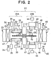
FIG. 2 is a diagram showing the structure of a sputtering
film deposition system for fabricating the antireflection
film;
FIG. 3 is a graph showing a spectral reflectance curve of
the antireflection film;
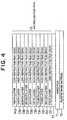
FIG. 4 is a section view showing the structure of an
spectacles plastic lens having a multi-layered antireflection
film;
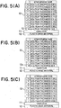
FIGs. 5(A), 5(B) and 5(C) are section views for comparing
a pre-treated spectacles plastic lens (A), an spectacles
plastic lens (B) with a pre-treatment layer having a thickness
out of a predetermined range, and an spectacles plastic lens
(C) on which no pre-treatment has been implemented;
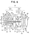
FIG. 6 is a diagram showing the structure of the main
part of a sputtering film deposition system to which a
thickness correcting mechanism is attached;
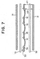
FIG. 7 is a longitudinal section view showing the state
of disposition of plastic base materials in a substrate holder
and the positional relationship among the substrate holder,
targets and thickness correcting plates;
FIG. 8 is a plan view showing a planar shape of the upper
thickness correcting plate;
FIG. 9 is a plan view showing a planar shape of the lower
thickness correcting plate; and
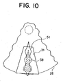
FIG. 10 is a diagram showing an non-erosion part in the
target.
Best Mode for Carrying Out the Invention
Preferred embodiments of the present invention will be
explained below based on the appended drawings.
An example of spectacles plastic lens will be cited as
plastic optical devices and an antireflection film formed on
the both sides of the spectacles plastic lens will be
explained in the present embodiment. Although the spectacles
plastic lens is suited most as the optical devices on which
the antireflection film of the present invention is formed,
the present invention is not limited only to that.
FIG. 1 is a diagrammatic section view showing a typical
example of the structure of the antireflection film and FIG. 2
is a structure diagram showing one example of a sputtering
film deposition system. Although the antireflection film is
formed on the both sides of the lens, FIG. 1 shows the
sectional structure of the antireflection film of only one
side for convenience of the explanation. The antireflection
film having the similar structure is formed also on the other
side of the lens.
A plastic base material 10 shown in FIG. 1 is a base
material of the spectacles plastic lens. CR-39 (diethylene
glycol bisallyl carbonate polymer nd = 1.499) is used for
example as the material of the plastic base material 10. A
hard film 11 is coated on the surface of the plastic base
material 10 in order to enhance the hardness thereof. Organic
silicon resin containing colloidal silica for example is used
for the hard film 11. The detail of the composition thereof
is described in Japanese Patent Publication No. Hei. 4-55615
for example.
It is noted that normally the plastic base material of
the spectacles plastic lens has curvature and has a curved
shape. However, FIG. 1 shows it in the form of a flat plate
for convenience of explanation. When the plastic base
material is curved, the film deposited thereon is curved along
the surface of the base material in general.
The antireflection film 13 to be coated on the plastic
base material 10 is formed on the hard film 11 because the
hard film 11 is coated thereon in the present embodiment. As
shown in FIG. 1, the antireflection film 13 of the present
embodiment is formed as a multi-layered film of ten layers for
example. Within the antireflection film 13, a film 131 at the
lowermost layer positioned on the side of the plastic base
material 10 is a high-refractive film. What is formed next on
the high-refractive film 131 is a low-refractive film 132.
Thereafter, films 133 through 140 are formed in serial order
while repeating the order of the high-refractive film and the
low-refractive film alternately. As a result, the films 131,
133, 135, 137 and 139 of the first, third, fifth, seventh and
ninth layers are laminated as the high-refractive films and
the films 132, 134, 136, 138 and 140 of the second, fourth,
sixth, eighth and tenth layers are laminated as the
low-refractive films, thus forming the antireflection film 13
having the multi-layered structure. The outside of the
low-refractive film 140 of the tenth layer is atmosphere.
In case of the present embodiment, the high-refractive
material constituting the above-mentioned high-refractive film
is metal oxide ZrO2 of zirconium (Zr) for example and the
low-refractive material constituting the above-mentioned
low-refractive film is metal oxide SiO2 of silicon (Si) for
example. Beside zirconium, metal oxides (TiO2, Ta2O5 and the
like) of titanium (Ti) and tantalum (Ta) may be used.
Further, metal oxide made from two or more alloys among
zirconium (Zr), titanium (Ti) and tantalum (Ta) may be used as
the high-refractive material. The high- and low-refractive
films are fabricated by utilizing the sputtering method as
described later. Therefore, targets of the high- and
low-refractive materials are prepared.
The high-refractive film may be also formed as a mixed
film containing the above-mentioned high-refractive material
and Si. The performance of the film such as the hardness and
durability may be improved by containing Si within the
high-refractive film. Such mixed film may be fabricated by
using the following two methods for example. The first method
is to include Si within the target of the high-refractive
material. The high-refractive film containing Si may be
deposited by the sputtering process using such target. The
second method is to provide a target of Si beside the target
of the high-refractive material. The mixed film may be formed
by sputtering the target of the high-refractive material and
that of the Si in the same time. The target of Si may be used
also as target of the low-refractive material.
In the antireflection film 13 having the multi-layered
structure formed as described above, preferably the thickness
of the high-refractive and low-refractive films of the
respective layers is set as follows, where λ is 500 nm
(nanometer).
The thickness of the high-refractive film of the first
layer is set so as to be included within the range from 0.075
λ to 0.085 λ, the thickness of the low-refractive film of the
second layer to be included within the range from 0.115 λ to
0.130 λ, the thickness of the high-refractive film of the
third layer to be included within the range from 0.177 λ to
0.199 λ, the thickness of the low-refractive film of the
fourth layer to be included within the range from 0.101 λ to
0.114 λ, the thickness of the high-refractive film of the
fifth layer to be included within the range from 0.102 λ to
0.115 λ, the thickness of the low-refractive film of the sixth
layer to be included within the range from 0.471 λ to 0.511 λ,
the thickness of the high-refractive film of the seventh layer
to be included within the range from 0.102 λ to 0.115 λ, the
thickness of the low-refractive film of the eighth layer to be
included within the range from 0.045 λ to 0.060 λ, the
thickness of the high-refractive film of the ninth layer to be
included within the range from 0.270 λ to 0.304 λ, and the
thickness of the low-refractive film of the tenth layer to be
included within the range from 0.244 λ to 0.275 λ. Within
those values, the most preferable value of the thickness of
each layer is the center value in each range.
The total thickness of the above-mentioned antireflection
film 13 is preferred to be included within the range of 4800
to 5800 angstrom and the total thickness of the low-refractive
films therein is preferred to be 3500 angstrom or more in
order to assure the durability such as the hardness and
abrasion resistance required as the antireflection film, the
adhesion as a film and others. In case of the present
embodiment, the thickness of the low-refractive film 136 of
the sixth layer positioned at the intermediate area is
thickened as compared to other films to achieve the required
thickness of the antireflection film 13 to satisfy the
requirements such as the hardness and durability. The film
positioned at the middle among the plurality of low-refractive
films is thickened based on the reason that such structure is
appropriate in view of stress and others of the film.
It is noted that a number of layers in the antireflection
film 13 is not limited to ten as described above. While the
number of layers in the antireflection film having the
multi-layered structure is preferred to be less from the
aspect of production of the film, it is set arbitrarily in
connection with the required film performance.
The plastic base material of the normal spectacles
plastic lens has curvature and a curved shape as described
before. When the antireflection film 13 having the
multi-layered structure shown in FIG. 1 is to be fabricated on
the curved plastic base material by using the sputtering
method as described later, a difference of distribution of
thickness is produced depending on the curvature of each part
of the plastic base material, thus causing non-uniformity of
the interference color and change in the interference color
due to oblique incidence. Then, in order to reduce such
troubles, it is preferred to design the antireflection film 13
as a film having a wide band characteristic.
Next, one example of a system for fabricating the
antireflection film 13 described above by utilizing the
sputtering method and a fabrication process will be explained
in outline with reference to FIG. 2. FIG. 2 shows a
longitudinal section view of the main part of the sputtering
film deposition system. This sputtering film deposition
system is capable of depositing the antireflection films 13
having the multi-layered structure on the both sides of the
plastic base material 10 in the same time.
The sputtering film deposition system may be roughly
divided into an introducing chamber 21 for carrying in an
object to be processed, a vacuum processing chamber
(sputtering film deposition chamber) 22 for depositing the
high-refractive films and low-refractive films alternately on
the both sides of the plastic base material 10 and a
preliminary processing chamber 23. The introducing chamber
21, the vacuum processing chamber 22 and the preliminary
processing chamber 23 are parted by gate valves 24 and 25.
The gate valves 24 and 25 are opened/closed at appropriate
timing in carrying in/out the object.
A substrate holder 26 carried into the inside of the
sputtering film deposition system via the introducing chamber
21 is set within the vacuum processing chamber 22 via the gate
valve 24. It is noted that a carriage mechanism for
transporting the substrate holder 26 is not shown in FIG. 2.
The substrate holder 26 has a shape of a disc for example. A
large number of base material holding holes 26a are formed in
the substrate holder 26. The plastic base materials 10 used
for the spectacles plastic lenses are disposed in those holes
26a. Because the base material holding holes 26a are opened
to the upper and lower sides, the plastic base materials 10
held by the base material holding holes 26a face to the spaces
above and under the substrate holder 26. As a result, the
above-mentioned antireflection films 13 may be formed on the
both sides of the plastic base material 10 by the sputtering
method.
The sputtering film deposition process in the vacuum
processing chamber 22 comprises a sputtering step for
depositing a metallic thin film and a transforming step for
transforming the metallic thin film deposited in the
sputtering step into an oxide thin film. Therefore, the
vacuum processing chamber 22 is provided with a sputtering
step area 22A and a transforming step area 22B in constructing
the system.
The substrate holder 26 is disposed horizontally by
supporting the center thereof with upper and lower supporting
members 27 and 28 within the vacuum processing chamber 22.
The upper and lower supporting members 27 and 28 are driven
vertically by a hydraulic cylinder or the like not shown and
can be freely rotated by a motor rotating mechanism built
therein. The substrate holder 26 is rotated at predetermined
speed by the rotating operation of the upper and lower
supporting members 27 and 28 in depositing the antireflection
film 13 on the plastic base material 10. Accordingly, while
the large number of plastic base materials 10 disposed on the
substrate holder 26 pass through the sputtering step area 22A
and the transforming step area 22B, the plastic base materials
10 are processed by the sputtering in the sputtering step area
22A and by the transforming in the transforming step area 22B.
Sputtering units are disposed above and below the
substrate holder 26 in the sputtering step area 22A. Each
sputtering unit comprises a target 31, a sputter electrode 32,
a sputter power supply 33, a sputter gas bottle 34, and a mass
flow (controller) 35. When the substrate holder 26 rotates
and the plastic base material 11 comes between the upper and
lower targets 31, the target substance emitted from the target
31 in the sputtering condition deposits on the both sides of
the plastic base material 11, thus forming thin films of the
target substance on the both surfaces of the plastic base
material 11. At this time, sputtering gas such as argon gas
is introduced from the sputter gas bottle 34 via the mass flow
35 so as to regulate the sputtering atmosphere.
In order to fabricate the aforementioned antireflection
film 13 in the sputtering film deposition process in the
vacuum processing chamber 22, the metal oxide ZrO2 is deposited
as the high-refractive film of the first layer and the metal
oxide SiO2 is deposited as the low-refractive film of the
second layer based on the above-mentioned sputtering step and
the transforming step described later Thereafter, the
high-refractive films ZrO2 and the low-refractive films SiO2
are formed alternately up to the tenth layer. In the
sputtering step area 22A, metal which is the source of each
metal oxide is deposited. In the first sputtering step for
depositing the high-refractive film 131 of the first layer,
the target made from zirconium Zr is prepared and Zr films are
formed on the both sides of the plastic base material 10. In
the sputtering step for depositing the low-refractive film 132
of the second layer, the target is exchanged to the other
target made from silicon Si and Si films are formed on the
both sides of the plastic base material 10 after the
sputtering. The antireflection film 13 may be thus formed by
laminating the high-refractive films and low-refractive films
alternately by exchanging the target to the high-refractive
material or to the low-refractive material. It is noted that
a mechanism for exchanging the targets is not shown in FIG. 2.
In the transforming step area 22B, induction coupled
plasma generating units are disposed above and below the
substrate holder 26. The induction coupled plasma generating
unit comprises a high-frequency discharging chamber 41, a
high-frequency coil 42, a matching box 43, a high-frequency
power supply 44, a reactive gas bottle 45 and a mass flow 46.
When the substrate holder 26 rotates and the plastic base
material 11 to be processed comes between the upper and lower
induction coupled plasma generating units, the plastic base
material 10 is exposed to plasma of oxygen introduced from the
reactive gas bottle 45 via the mass flow 46 to oxidize the
metal (Zr or Si) deposited in the sputtering step to transform
into oxide (ZrO2 or SiO2).
As described above, the antireflection films 13 having
the multi-layered structure composed of the ZrO2
(high-refractive film) and SiO2 (low-refractive film) films
shown in FIG. 1 are formed on the both sides of the plastic
base material 10 by repeating the sputtering step and the
transforming step while exchanging the targets on the both
sides of the large number of plastic base materials 10 on the
substrate holder 26 set to be freely rotatable within the
vacuum processing chamber 22.
It is noted that a shielding member 47 for separating the
sputtering step area 22A from the transforming step area 22B
is provided within the vacuum processing chamber 22.
The following is one example as to conditions for forming
the ZrO
2 film, i.e., the high-refractive film, in the
sputtering step in the sputtering film deposition system:
The following is one example as to conditions for forming
the SiO
2 film, i.e., the low-refractive film, in the sputtering
step in the sputtering film deposition system:
The following is the performance of the antireflection
film 13 thus obtained on the spectacles plastic lens having
such antireflection film in the initial period after its
formation and the performance thereof after one month in
constant temperature and humidity.
As the performance of the film, its abrasion resistance,
adhesion, alkali resistance, heat resistance, acid resistance,
artificial perspiration resistance and interference color were
measured and evaluated by the following methods:
The following is the performance of the
antireflection
film 13 in the initial period after its formation based on the
foregoing measurement and evaluation:
The following is the performance of the
antireflection
film 13 after one month in the environment of constant
temperature and humidity based on the foregoing measurement
and evaluation,
FIG. 3 shows a measured example of a spectral reflectance
curve of the antireflection film 13. As it is apparent from
this spectral reflectance curve, the low reflectance has been
achieved in a wide wavelength range of about 420 to 740 nm,
i.e., the wide band antireflection film has been realized.
The reflectance is relatively high in the wavelength range of
about 480 to 550 nm in particular.
Further, the above-mentioned antireflection film has the
greenish interference color by setting its dominant wavelength
range as 480 to 550 nm, excitation purity range as 10 to 30 %
and luminous reflectance as 0.7 to 1.8 %. While luminous
reflectance and chromaticity are used in general in indicating
a color of a reflecting object (the interference color of the
antireflection film on the surface of the lens in case of the
present embodiment), dominant wavelength and excitation
purity are used in monochromatically indicating the
chromaticity. Here, the luminous reflectance is expressed by
the ratio of luminous flux reflected from an object to
luminous flux incident on the object, corresponds to the
Y-value of the tristimulus values and is given by the
following expression:
R = 380 780 Pλ Rλ Vλ dλ / 380 780 Pλ Vλ dλ
where, R is the luminous reflectance, Pλ is spectral
composition of incident light, Vλ is relative luminous
efficiency and Rλ is spectral reflectance.
It becomes the criterion for judging how bright the light
having the spectral composition Pλ looks when it enters a lens.
The dominant wavelength and the excitation purity are
both elements for indicating the chromaticity by monochromatic
representation. The wavelength corresponding to a point where
a line connecting a point represented by chromaticity
coordinates on a chromaticity diagram and a light source
intersects with a spectrum locus is called the dominant
wavelength specifically.
The antireflection film of the present embodiment having
the spectral reflectance curve shown in FIG. 3 has had 508 nm
of dominant wavelength, 22 % of excitation purity, 0.963 % of
luminous reflectance and the greenish interference color.
Although the method for forming the antireflection film
by using the sputtering method has been explained above, the
similar antireflection film having the multi-layered structure
may be fabricated by other methods such as a vacuum
evaporation method and a CVD method.
Further, although the antireflection films having the
multi-layered structure have been formed on the both sides of
the base material of the spectacles plastic lens in the
present embodiment, the antireflection film may be formed only
one side in case of other plastic optical devices.
Still more, although the first layer of the
antireflection film 13 has been the high-refractive film 131
in the present embodiment, it needs not be the first layer
strictly. For instance, another film may be present between
the hard film 12 and the high-refractive film 131.
Accordingly, it will do if the high-refractive film 131 is
substantially the first layer in the antireflection film 13.
This point will be detailed further in a second embodiment.
According to the plastic optical devices described above,
the antireflection film having the multi-layered structure is
formed by depositing the high-refractive material as the first
layer and the low-refractive material as the second layer and
by laminating the high-refractive materials and low-refractive
materials alternately on the both sides of the plastic base
material for example by using the sputtering method and the
thickness of the low-refractive material at the middle of the
antireflection film is thickened relatively, so that the
antireflection film having the highly evaluated film
performance may be realized. Further, because the
antireflection film is formed as the wide band film, it can
reduce the non-uniformity of interference color which is
caused by the difference of distribution of thickness
dependent on the curvature in the deposition by the sputtering
method and the change in the interference color caused by
oblique incidence, when the plastic base material has the
curvature. Still more, it allows the greenish interference
color to be obtained stably and the antireflection film which
is excellent eye-physiologically and aesthetically and highly
valuable commercially to be fabricated.
Next, the second embodiment will be explained with
reference to FIGs. 4 and 5. In this present embodiment, the
plastic optical devices is limited to be the spectacles
plastic lens. The film structure formed on the surface of the
plastic base material 10 is improved in order to prevent the
occurrence of cracks. The elements in FIGs. 4 and 5
substantially identical with those elements explained in FIG.
1 will be denoted by the same reference numerals and the
repeated detailed explanation thereof will be omitted here.
In FIG. 4, the reference numeral (10) denotes a plastic
base material, (11) a hard film, and (13) an antireflection
film. The plastic base material 10, the hard film 11 and the
antireflection film 13 are the same ones with those explained
in the foregoing embodiment. The antireflection film 13 is
actually formed on the hard film 11. More specifically, a
super-thin film 12 of SiO(2-x) (x = 0, 1) is formed as a
pre-treatment layer between the hard film 11 and the
antireflection film 13. That is, the SiO(2-x) super-thin film
12 is formed as the pre-treatment layer when forming the
antireflection film 13 having the multi-layered structure on
the plastic base material 10. The thickness of the super-thin
film 12 is preferred to be included within the range from 15
to 50 angstrom. Stress balance between the interface of the
plastic base material 10 and the high-refractive film 131
changes appropriately by providing the super-thin film 12 as
the pre-treatment layer. As a result, it becomes possible to
prevent cracks from occurring on the antireflection film 13
caused by humidity and pressure and to keep the appearance as
the spectacles plastic lens well. Further, the adhesion
between the antireflection film 13 and the plastic base
material 10 may be kept high naturally. It is noted that
there arises a problem that the adhesion drops when the
thickness of the super-thin film 12 exceeds 50 angstrom.
Next, the antireflection film (A) having the
above-mentioned structure will be compared with two
antireflection films (B) and (C) having other structures with
reference to FIG. 5. The antireflection film 13 having the
multi-layered structure in FIG. 5(A) comprises ten layers of
high-refractive films and low-refractive films. Numerals 1
through 10 at the left edge of the figure of the
antireflection film 13 indicate the layer Nos. The thickness
of the respective layers from the high-refractive film of the
first layer to the low-refractive film of the tenth layer are
0.08 λ , 0.12 λ, 0.19 λ, 0.11 λ, 0.11 λ, 0.49 λ, 0.11 λ, 0.05
λ, 0.29 λ and 0.26 λ as described in the figure. These
thicknesses are included within the aforementioned ranges of
thickness of the respective layers. The above-mentioned
structure of the antireflection film 13 is the same also in
the antireflection films in FIGs. 5(B) and (C).
In the arrangement in FIG. 5(A), the antireflection film
13 is formed on the plastic base material 10 on whose surface
the hard film 11 is coated via the SiO(2-x) super-thin film 12
having the thickness of 15 angstrom. That is, the SiO(2-x)
super-thin film 12 is formed as the pre-treatment film. It is
noted that the upper side of the low-refractive film of the
tenth layer is atmosphere.
In the arrangement in FIG. 5(B), an SiO(2-x) super-thin
film 12a is formed in the same manner as the pre-treatment
film between the antireflection film 13 and the plastic base
material 10 on whose surface the hard film 11 is coated.
However, the thickness of the super-thin film 12a is 80
angstrom, which is greater than 50 angstrom and is not
included within the aforementioned range.
In the arrangement in FIG. 5(C), no SiO(2-x) super-thin
film is formed between the antireflection film 13 and the
plastic base material 10 on whose surface the hard film 11 is
coated. That is, no pre-treatment by means of the
above-mentioned super-thin film is implemented. The
antireflection film 13 is formed directly on the plastic base
material 10 on which the hard film 11 is coated.
Next, the comparison result of the film performance of
the respective spectacles plastic lenses having the structures
shown in FIGs. 5(A), 5(B) and 5(C) will be explained. In this
comparison, the spectacles plastic lenses having the
respective structures shown in FIGs. 5(A), 5(B) and 5(C) were
fabricated, were fitted into spectacles frames and were left
for 24 hours within a constant temperature and humidity
furnace at 90 % of humidity and 40°C of temperature. Then,
the adhesion of the antireflection film and the appearance
(whether or not cracks have occurred) of the spectacles
plastic lenses were checked. It is noted that the "adhesion"
was evaluated by crosscutting the surface of the spectacles
plastic lens with the antireflection film into 100 divisions
at intervals of 1 mm, pasting cellophane tape strongly, and
then peeling it off rapidly to check whether or not the
antireflection film is peeled off.
As a result, the adhesion was 100/100, no peeling was
seen and the appearance did not change in the spectacles
plastic, lens having the structure shown in FIG. 5(A). In the
spectacles plastic lens having the structure shown in FIG.
5(B), the adhesion was 0/100, all of the antireflection films
were peeled and the performance was extremely bad. However,
the appearance did not change. In the spectacles plastic lens
having the structure shown in FIG. 5(C), although the adhesion
was 100/100 and was good, it caused a problem as for the
appearance that cracks occur from the edge portion of the
lens.
As it is apparent from the above comparison, the
antireflection film 13 having the super-thin film 12 coated as
the pre-treatment film on the spectacles plastic lens (the
plastic base material 10) had the high performance in terms of
the adhesion and appearance. In addition to that, the
antireflection film 13 exhibits the excellent performance also
in terms of the abrasion resistance, alkali resistance, heat
resistance, acid resistance and artificial perspiration
resistance. This antireflection film also achieves the low
reflectance in a wide wavelength range of about 420 to 740 nm
in the spectral reflectance curve, thus realizing the wide
band antireflection film. The reflectance is relatively high
in the wavelength range of about 480 to 550 nm in particular.
Further, the above-mentioned super-thin film and the
antireflection film present the greenish interference color by
setting the dominant wavelength to be 480 to 550 nm, the
excitation purity to be 10 to 30 % and the luminous
reflectance to be 0.7 to 1.8 %.
According to the spectacles plastic lens described above,
because the SiO(2-x) super-thin film 12 is formed as the
pre-treatment layer when forming the multi-layered
antireflection film whose first layer is the high-refractive
film, it is possible to prevent cracks from occurring and to
improve the appearance as the spectacles plastic lens. It is
also possible to obtain the greenish interference color stably
by the super-thin film and others and to fabricate the
spectacles plastic lens which is excellent eye-physiologically
and aesthetically and highly valuable commercially.
Next, a third embodiment will be explained with reference
to FIGs. 6 through 10. In the present embodiment, a mechanism
for enhancing the uniformity of the thickness of the thin
films formed on the both sides of the plastic base material 10
is added in the arrangement of the second sputtering film
deposition system described above. The elements in FIG. 6
substantially the same with those elements explained in FIG. 2
will be denoted by the same reference numerals and their
detailed repeated explanation will be omitted here. It is
noted that the material of the base material 10 is not limited
to plastic and may be glass for example.
The plastic base material 10 is the base material of the
spectacles plastic lens having a meniscus shape. The
antireflection film is deposited on the both sides of the
plastic base material 10 as the spectacles plastic lens. The
antireflection film is the multi-layered film in which the
high-refractive films (e.g., ZrO2) and the low-refractive films
(e.g., SiO2) are laminated alternately as described before.
Because the plastic base material 10 is an spectacles plastic
lens, the both sides thereof have curvature. In concrete, one
surface of the plastic base material 10 is a concave surface
and the other surface is a convex surface. The plastic base
material 10 is set horizontally in the substrate holder 26.
In this state, normally the plastic base material 10 is set
while facing the concave surface up and the convex surface
down.
The structure and operation of the sputtering film
deposition system are the same as described before. The
structure specific to the sputtering film deposition system
shown in FIG. 6 is that a thickness correcting mechanism is
provided within the sputtering step area 22A of the vacuum
processing chamber 22.
The thickness correcting mechanism comprises thickness
correcting plates 51 and 52 disposed between the respective
targets 31 and the substrate holder 26 in the sputtering step
area 22A. It is noted that in FIG. 6, structures for
supporting the thickness correcting plates 51 and 52 are not
shown. An arbitrary structure may be adopted for the
supporting structure by utilizing the empty space.
Functionally, the thickness correcting plates 51 and 52 are
mask members for covering the plastic base material 10 which
has come to the position facing to the center part of the
target 31 by the rotating operation of the substrate holder 26
by a desirable shape (covering pattern). Sputtering particles
from the target 31 may be shielded partly, the thickness of
the thin film deposited on the surface of the respective
plastic base materials 10 may be corrected and the thickness
of the film on the surface may be equalized by covering the
several plastic base materials 10 by the thickness correcting
plates which function as the mask members having the desirable
covering pattern.
The thickness correcting plate will be explained in
detail below with reference to FIGs. 7 through 9. FIG. 7 is
an enlarged view showing the disposition of the plastic base
materials 10 set on the substrate holder 26 and the
relationship between the upper and lower targets 31 and the
thickness correcting plates 51 and 52 more concretely, FIG. 8
shows one example of the planar shape of the thickness
correcting plate 51 and FIG. 9 shows one example of the planar
shape of the thickness correcting plate 52.
In FIG. 7, the direction indicated by an arrow 53 is the
direction toward the center of rotation of the substrate
holder 26, d1 is a distance between the substrate holder 26
and the lower target 31 and d2 is a distance between the
plastic base material 10 and the lower target 31. As it is
apparent from the figure, the plastic base materials 10 are
disposed on the base material holding holes 26a created
through the substrate holder 26 via fittings 54 while facing
the concave surface up and facing the convex surface down.
The disposition of the plastic base material 10 is set so that
the lowermost point of the convex surface of the plastic base
material 10 comes to the position almost at the middle between
the upper and lower targets 31, and thereby, the position of
the substrate holder 26 is determined. Accordingly, the
above-mentioned distance d2 is set between the lower target 31
and the lowermost point of the lower face of the plastic base
material 10. Further, the distance d1 between the substrate
holder 26 and the lower target 31 is slightly greater than the
distance between the substrate holder 26 and the upper target
31.
The plurality of plastic base materials 10 are disposed
on concentric circles 55, 56 and 57 in the substrate holder 26
as shown in FIG. 8. The three concentric circles are utilized
in the present embodiment. Further, as it is apparent from
FIGs. 8 and 9, the planar shape of the upper and lower targets
31 preferably have a trapezoidal shape having a short edge at
the center side and a long edge at the peripheral side.
The above-mentioned thickness correcting plate 51 having
the planar shape as shown in FIG. 8 is disposed between the
upper target 31 and the plurality of plastic base materials 10
set on the substrate holder 26 in the arrangement as described
above. The thickness correcting plate 51 is disposed so that
its longitudinal direction is oriented to the direction (the
radial direction) of a straight line connecting the center
part and the peripheral part in the substrate holder 26. In
the thickness correcting plate 51, preferably, length in the
circumferential direction of devices corresponding to the
concentric circles 55-57 (where the plastic base materials are
disposed or present) is longer than length in the
circumferential direction of the other devices, and further
the length of the devices corresponding to the concentric
circles 55-57 in the thickness correcting plate 51 is set so
as to become small gradually from the peripheral part to the
center part. Thereby, a predetermined range of the upper
faces (concave surfaces) of the plastic base materials 10
which have come to the position facing almost to the center
part of the upper target 31 by the rotatable substrate holder
26 are covered by the thickness correcting plate 51. As a
result, the thickness of the thin film deposited on the upper
faces (concave surfaces) of the plastic base materials 10 are
equalized, because they are corrected by the masking action of
the thickness correcting plate 51. It is noted that the
planar shape of the thickness correcting plate 51 is not
limited only to that shown in FIG. 8.
Similarly, the above-mentioned thickness correcting plate
52 having the planar shape as shown in FIG. 9 is disposed
between the lower target 31 and the plurality of plastic base
materials 10 the substrate holder 26. The thickness
correcting plate 52 is disposed so that its longitudinal
direction is oriented to in the direction (the radial
direction) of a straight line connecting the center part and
the peripheral part in the substrate holder 26, and
preferably, length in the circumferential direction of parts
corresponding to the intermediate portions of the concentric
circles 55-57 (boundaries between the plastic base materials)
is longer than length in the circumferential direction of the
other parts. Thereby, a predetermined range of the lower
faces (convex surfaces) of the plastic base materials 10 which
have come to the position facing almost to the center part of
the lower target 31 by the rotatable substrate holder 26 are
covered by the thickness correcting plate 52. As a result,
the thickness of the thin film deposited on the lower faces
(convex surfaces) of the plastic base materials 10 are
equalized, because they are corrected by the masking action of
the thickness correcting plate 52. It is noted that the
planar shape of the thickness correcting plate 52 is not
limited only to that shown in FIG. 9.
In another point of view, the thickness correcting plates
51 and 52 function as the mask members having the following
actions. That is, the target 31 having the trapezoidal shape
is normally provided with a peculiar magnet structure (not
shown) and creates an non-erosion part 58 similar to the shape
of isosceles triangle at the center part of the target
according to the film deposition action based on the
sputtering. When such non-erosion part 58 exists on the
target 31, abnormal discharge is liable to occur due to
reaction products deposited on the target surface in the
non-erosion part 58. As a result, the reaction products fly
as particles from the non-erosion part 58 and arrive and
adhere on the surface of the plastic base material 10.
However, because the thickness correcting plates 51 and 52 are
disposed between the substrate holder 26 and the upper and
lower targets 31 as described above in the above-mentioned
sputtering film deposition system so that the thickness
correcting plates cover the plastic base materials 10 facing
to the targets, they interfere the particles flying from the
non-erosion part 58 and prevent the particles from arriving to
the surfaces of the plastic base materials 10.
The above-mentioned thickness correcting mechanism allows
the thickness of the thin film on the surface of the optical
lens base material to be equalized and the favorable
distribution of thickness to be realized in depositing the
thin films on the both sides or on one side of the optical
lens base material by the sputtering film deposition system by
using the sputtering method. Further, the thickness
correcting plates allow the particles flying from the
non-erosion portion of the targets to be interfered.
Industrial Applicability
The present invention is suitable for coating the
antireflection film having the highly evaluated film
performance on the plastic optical devices. The
antireflection film is formed as a wide band film and reduces
the non-uniformity of interference color caused by the
difference of distribution of thickness and the change in the
interference color caused by oblique incidence when the
plastic base material has curvature. The present invention
allows the greenish interference color to be obtained stably
and the antireflection film which is excellent
eye-physiologically and aesthetically and is highly valuable
commercially to be fabricated. In case of the spectacles
plastic lens, the super-thin film of SiO(2-x) prevents cracks
from occurring on the antireflection film as the pre-treatment
layer. The thickness correcting plates of the thickness
correcting mechanism equalize the thickness of the thin film
deposited on the surface of the plastic base material by the
sputtering method.