EP0928084A2 - Universal modem for digital video, audio and data communications - Google Patents
Universal modem for digital video, audio and data communications Download PDFInfo
- Publication number
- EP0928084A2 EP0928084A2 EP98124048A EP98124048A EP0928084A2 EP 0928084 A2 EP0928084 A2 EP 0928084A2 EP 98124048 A EP98124048 A EP 98124048A EP 98124048 A EP98124048 A EP 98124048A EP 0928084 A2 EP0928084 A2 EP 0928084A2
- Authority
- EP
- European Patent Office
- Prior art keywords
- modulation
- format
- modem
- channel
- demodulator
- Prior art date
- Legal status (The legal status is an assumption and is not a legal conclusion. Google has not performed a legal analysis and makes no representation as to the accuracy of the status listed.)
- Withdrawn
Links
Images



Classifications
-
- H—ELECTRICITY
- H04—ELECTRIC COMMUNICATION TECHNIQUE
- H04B—TRANSMISSION
- H04B1/00—Details of transmission systems, not covered by a single one of groups H04B3/00 - H04B13/00; Details of transmission systems not characterised by the medium used for transmission
- H04B1/005—Details of transmission systems, not covered by a single one of groups H04B3/00 - H04B13/00; Details of transmission systems not characterised by the medium used for transmission adapting radio receivers, transmitters andtransceivers for operation on two or more bands, i.e. frequency ranges
-
- H—ELECTRICITY
- H04—ELECTRIC COMMUNICATION TECHNIQUE
- H04B—TRANSMISSION
- H04B1/00—Details of transmission systems, not covered by a single one of groups H04B3/00 - H04B13/00; Details of transmission systems not characterised by the medium used for transmission
- H04B1/38—Transceivers, i.e. devices in which transmitter and receiver form a structural unit and in which at least one part is used for functions of transmitting and receiving
- H04B1/40—Circuits
- H04B1/403—Circuits using the same oscillator for generating both the transmitter frequency and the receiver local oscillator frequency
- H04B1/406—Circuits using the same oscillator for generating both the transmitter frequency and the receiver local oscillator frequency with more than one transmission mode, e.g. analog and digital modes
-
- H—ELECTRICITY
- H04—ELECTRIC COMMUNICATION TECHNIQUE
- H04L—TRANSMISSION OF DIGITAL INFORMATION, e.g. TELEGRAPHIC COMMUNICATION
- H04L1/00—Arrangements for detecting or preventing errors in the information received
- H04L1/0001—Systems modifying transmission characteristics according to link quality, e.g. power backoff
- H04L1/0002—Systems modifying transmission characteristics according to link quality, e.g. power backoff by adapting the transmission rate
- H04L1/0003—Systems modifying transmission characteristics according to link quality, e.g. power backoff by adapting the transmission rate by switching between different modulation schemes
-
- H—ELECTRICITY
- H04—ELECTRIC COMMUNICATION TECHNIQUE
- H04L—TRANSMISSION OF DIGITAL INFORMATION, e.g. TELEGRAPHIC COMMUNICATION
- H04L1/00—Arrangements for detecting or preventing errors in the information received
- H04L1/0001—Systems modifying transmission characteristics according to link quality, e.g. power backoff
- H04L1/0023—Systems modifying transmission characteristics according to link quality, e.g. power backoff characterised by the signalling
- H04L1/0025—Transmission of mode-switching indication
-
- H—ELECTRICITY
- H04—ELECTRIC COMMUNICATION TECHNIQUE
- H04L—TRANSMISSION OF DIGITAL INFORMATION, e.g. TELEGRAPHIC COMMUNICATION
- H04L1/00—Arrangements for detecting or preventing errors in the information received
- H04L1/0001—Systems modifying transmission characteristics according to link quality, e.g. power backoff
- H04L1/0023—Systems modifying transmission characteristics according to link quality, e.g. power backoff characterised by the signalling
- H04L1/0032—Without explicit signalling
-
- H—ELECTRICITY
- H04—ELECTRIC COMMUNICATION TECHNIQUE
- H04L—TRANSMISSION OF DIGITAL INFORMATION, e.g. TELEGRAPHIC COMMUNICATION
- H04L27/00—Modulated-carrier systems
- H04L27/0008—Modulated-carrier systems arrangements for allowing a transmitter or receiver to use more than one type of modulation
-
- H—ELECTRICITY
- H04—ELECTRIC COMMUNICATION TECHNIQUE
- H04L—TRANSMISSION OF DIGITAL INFORMATION, e.g. TELEGRAPHIC COMMUNICATION
- H04L27/00—Modulated-carrier systems
- H04L27/0012—Modulated-carrier systems arrangements for identifying the type of modulation
-
- H—ELECTRICITY
- H04—ELECTRIC COMMUNICATION TECHNIQUE
- H04L—TRANSMISSION OF DIGITAL INFORMATION, e.g. TELEGRAPHIC COMMUNICATION
- H04L27/00—Modulated-carrier systems
- H04L27/26—Systems using multi-frequency codes
- H04L27/2601—Multicarrier modulation systems
Definitions
- This invention relates to modulators and demodulators and, more particularly, to a universal modem which is configurable to process one of a number of modulation formats.
- programm material in video, data or audio form is formatted by a channel encoder so as to be transmittable by Vestigial Side Band modulation or VSB which is typical for over-the-air television transmissions.
- VSB Vestigial Side Band modulation
- Quadrature Amplitude Modulation or QAM is typically used for cable transmission
- Quadrature Phase Shift Keying of QPSK is generally used in satellite communication.
- discrete multitone or DMT techniques are typically used for telephone landline signaling such as with Asymmetric Digital Subscriber Lines or ADSL.
- the source coding unit is set up to code the video source material in one of the four above-mentioned modulation formats.
- the receive side in order for a receiver to decode all of the above-mentioned formats discrete VLSI chips or detectors can be provided in parallel, with the outputs going to source decoding.
- Modulation format can be determined in some instances by the channel to which the receiver is tuned, although this can vary from country to country.
- VSB modulation is used, with the VSB demodulator switched to source decoding.
- QAM modulation is used, with the output of the QAM demodulator switched to source decoding.
- QPSK modulation is used, with the QPSK demodulator switched to source decoding, whereas for telephone line usage, assuming a channel indicating landline transmission, it is the DMT output of a demodulator which is switched to source decoding.
- duplicating modulators are likewise expensive and error-prone in much the same way as described above with respect to demodulators.
- specialty services such as date to be provided on different channels, oftentimes the modulation format is different from that of the main transmission. To provide such additional services ordinarily would require separate modulators having the expected cost impact.
- a universal modem is provided which is based on reconfigurable logic for its demodulator as well as its modulator.
- a controller is used to control the modulation type on both the transmit and receive side with means provided to sense channel noise and change the modulation type accordingly.
- a host computer at the receive side detects the modulation type and reconfigures the demodulator in universal modem to demoulate the format of the incoming signal.
- a host computer detects the modulation type of the incoming signal by detecting the channel to which the receiver is tuned and setting the demodulator to the expected format.
- the universal modem is reconfigured to the expected format of signals on that channel. This is done on an a priori basis since different groups of channels have different standardized formats.
- the host computer can detect the format of the incoming signal by detecting a flag in the header of the incoming data stream indicating modulation type, assuming one is loaded into the header at the transmit side.
- This type of demodulation selection does not require a priori knowledge of the correlation of channel with modulation type.
- different channels are assigned to different types of service which makes this alternative method of ascertaining the channel modulation type attractive.
- the above requires that a modulation type flag be generated in the source coding at the transmit side.
- Video information is source coded in MPEG in which 188 bytes of information are transmitted as a packet.
- Channel coding which defines the modulation format is imposed on top of the source coding to provide error correction which adds typically 20 more bytes of information to the data stream.
- the universal modem is also applicable to such diverse areas as cellular, PCS and other wireless services to provide automatic reconfiguring of a transceiver to permit its use across different formats.
- This is especially useful with cellular phone formats CDPD, CDMA, TDMA, FDMA and GSM referring respectively to cellular digital packet data, code division multiplexing, time-division multiplexing, frequency-division multiplexing, and the global mobile system type of modulation.
- a universal modem within the phone can detect the change and reconfigure the demodulator side of the modem.
- the universal modem can be reconfigured in the transmit mode to appropriately format the cellular transmission. It will of course be appreciated that the universal modem can be used with any type of RF transceiver roaming from one area to another where different formats are used, regardless of the type of service that is authorized.
- the universal modem is applicable to any kind of digital modulation method. For instance, it can be applied to digital terrestrial broadcasting utilizing the OFDM or Orthogonal Frequency Division Multiplexing method scheduled for use in Europe Japan and/or other countries.
- the demodulation section of the modem involves an analog-to-digital converter to provide a digital bit stream to a demodulator which is software-reconfigured in accordance with the out-put of a configuration RAM.
- circuit blocks, elements or modules within the demodulator are linked up to provide a particular type of carrier recovery in accordance with the output of the configuration RAM.
- the demodulator is layered, with each layer containing a different carrier recovery circuit. The configuration RAM can call for a given type of demodulation merely by activating one of the layers.
- the configuration of the demodulator can be fixed by providing it with blocks, elements or modules that are connected in a particular way on the fly in response to the output of a configuration RAM under the control of a configuration controller.
- the software-configurable demodulator can be implemented in software using a general purpose microprocessor. Note that the above software reconfiguration techniques utilized for the demodulator can likewise be used for a software-configurable modulator.
- the output of the configuration RAM may also be utilized to reconfigure an equalizer coupled to the output of the demodulator.
- the demodulator when no follow-on signal processing is required, the only element that is to be reconfigured is the demodulator. It will be noted that equalizers are in general used to correct intersymbol interference, whereas in television application, equalizers are used to cancel ghost images.
- flags can be used on the transmission which are detected at the receive side.
- the channel to which the receiver is tuned can be detected.
- a smart card or other similar device can be used to set the modulation type or format at the receive side.
- An additional way of detecting modulation type is to demodulate an incoming data stream using all possible formats, detecting the error and setting the demodulator to the modulation type having the lowest error.
- a universal modem has a software-configurable modulator/demodulator which accommodates different modulation formates such as those associated with terrestrial, cable, phone line, satellite and wireless communications to be transmitted and received through a single device in which the modem has reconfigurable logic to accommodate the format of the signals being received or transmitted.
- the system tracks channel noise and changes modulation format at both the transmit and receive sides of the system through the use of a controller that controls both sides.
- the modulator or demodulator can be used separately or the two units can be combined and used for transceivers, with either the same software configuring both the modulator and demodulator, or with different software used for the two units.
- the universal modem detects the modulation format of the incoming signal and reconfigures the logic of this software-configurable demodulator to output demodulated digital data for further processing.
- the transmit mode information to be transmitted is provided with the appropriate modulation format by setting a software-configurable modulator in the universal modem to the particular format.
- the incoming signal in the receive mode is A-D converted, with a host processor utilized to detect the type of modulation associated with the incoming signal and through a configuration controller configures a random access memory which is coupled to the software-configurable demodulator.
- the demodulated signal is passed through an equalizer, a Trellis Decoder and Reed-Solomon Decoder to provide an appropriate filtered and level-adjusted digital signal that is coupled to the next processing stage.
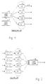
- source coding 10 takes video content from a video source 12 and encodes it into bit streams, whereupon the output of source coding unit 10 is applied in parallel to modulators 14, 16, 18 and 20 respectively VSB, QAM, QPSK and DMT modulators.
- modulators 14, 16, 18 and 20 respectively VSB, QAM, QPSK and DMT modulators.
- the formats for VSB, QAM and QPSK modulation techniques are described in K. Blair Benson, Television Engineering Handbook, Revised Edition, MCGraw-Hill, 1992.
- VSB was the format originally used to transmit over-the-air video signals.
- Vestigial Side Band Modulation was deemed to be most efficient modulation method, whereas, with respect to cable, Quadrature Amplitude Modulation gave superior performance.
- modulation format there exist numerous modulation schemes which must be accommodated by a universal modem.
- an incoming signal is down converted by RF-IF converters, here illustrated by reference characters 22, 24, 26 and 28, coupled to respective demodulators 32, 34 and 36.
- the VSB and QAM modulators are available from major television manufacturers, as well as being under development in a joint development program between Mitsubishi Electronics America and Lucent Technologies, Inc.
- QPSK demodulators are available from Philips Semiconductors, Part No. TDA8040T, among others.
- DMT-based ADSL equipment is described in "Notice to the Industry: ADSL Equipment", Bellcore Digest of Technical Information, June, 1993, p. 40.
- the outputs of these demodulators are switched to a source decoding unit 38, such as the Mitsubishis MH-1000D.
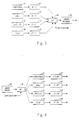
- a universal modem 40 which is software-reconfigurable has an input either a terrestrial signal 42, a cable signal 44, a satellite signal 46 or a landline signal 48, each with its own unique modulation format.
- the signals are coupled to respective RF-IF converters, 50,52, 54 and 56.
- the output of the universal modulator is in turn coupled to conventional source decoding 58.
- the universal modem is reconfigurable depending either on the channel to which the receiver is turned, or on detection of format flags.
- the universal modem is thus provided with configuration control signals derived either through a priori knowledge of the modulation type associated with a channel or actual detection of format flags.
- source coding 60 is coupled to universal modem 40 which in turn configures the modulator in the modem to output bit streams having the required modulation format dependent on the media, namely, terrestrial 42, cable, 44, satellite 46 and landline 48.
- the modulator is software-configurable, which eliminates the requirement for a plurality of modulators.
- modem 40 reformats the program material or video source from source coding 60 so as to put the material into a modulation format which is compatible with the particular medium over which the information is to be transmitted.
- modem 40 performs function of channel coding, with the channel dictating the particular modulation format.
- the output of modem 40 is provided to that IF-RF converter 62, 64, 66 and 68 required for the associated media.
- the role of the universal modem is of a network interface module.
- it allows the user to send signals, such as request for data or audio/video services, via different return channels having different modulation platforms. This not only increases the flexibility and mobility of the device, it also benefits the optimization of return channel bandwidth and utilization efficiency.
- the universal modem when used in broadcast services, provides a low cost modulation platform which can be changed under software control from one modulation format to another. This benefits regional stations which typically have a small number of channels to provide service with, but obtain their programs from more than one service provider and network involving multiple modulation types.
- the advantages for PCS referred to hereinabove include the ability to instantly switch from one format to another when roaming, depending on the area the cell phone is in, thus to switch from TDMA to CDMA and vice versa as an example.
- the CDMA system is described in U.S. Patent 5,103,459 entitled SYSTEM AND METHOD FOR GENERATING SIGNAL WAVE FORMS IN A CDMA CELLULAR TELEPHONE SYSTEM.
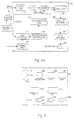
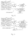
- the receive side of the universal modem includes an input 70 from tuner 71 which is coupled to a front end 72 whose primary purpose is level adjustment, amplification and filtering of the incoming signals from the tuner.
- the tuner is set to a given channel by channel select 73.
- the output of front end 72 is coupled to A-D converter 82, and thence to software-configurable demodulator 84.
- the header of the input signal is stripped off and provided to a host processor 74 which determines from flags in the header the modulation format type.
- the host processor can determine the modulation format through channel input 76 from the channel select 73. In either event, the output of the host processor specifies the modulation format to a configuration controller 78, the purpose of which is to select from a configuration RAM 80 the appropriate demodulation mode to be downloaded to demodulator 84.
- demodulator 84 is provided with an array of gates, arithmetic logic units or ALUs, registers and other circuit blocks, elements or modules which can be connected together to provide a circuit to recover the associated carrier.
- the demodulator is configured in layers, with each layer containing gates and logic as well as filtering to provide a circuit specially tailored for carrier recovery of a different modulation format type.
- the configuration RAM therefore merely selects which of the layers is to be activated, thereby, taking advantage of the embedded logic in each of the layers.
- the universal modem hardware is realized in a VLSI chip, using the logic implemented with DRAM technology and hardware-software codesign.
- the communication between the configuration control an the host processor is provided by an I 2 C bus.
- the configuration RAM can be implemented with either DRAM- or SDRAM technology, with the latter ensuring faster execution, which is desirable if the amount of data to be stored is very large.
- the building blocks, elements or modules within the demodulator are quite similar across the entire spectrum of modulation formats. This being the case, these blocks, elements or modules are capable of being connected together in a different manner for each of the modulation types.
- the configuration RAM 80 instructs demodulator 84 as to how it is to be reconfigured for the particular modulation type.
- the output of demodulator 84 is coupled to an equalizer 86 which, in one application, is utilized for ghost cancellation or to reject inter-symbol interference.
- the output of equalizer 86 is coupled to a Trellis Decoder, the purpose of which is to eliminate errors in the bit level of the incoming signal, whereas a Reed-Solomon Decoder 90 is utilized to remove byte level errors.
- the output of decoder 90 is coupled to I/O 92 which forms the output of the demodulation section of the subject universal modem.
- the universal modem in one embodiment, has an input 71 coupled to an I/O stage 73, which is in turn coupled to an R-S encoder 75. This encoder is in turn coupled to a Trellis encoder 77 which is then coupled to a software-configurable modulator 79. The output of modulator 79 is coupled to a digital-to-analog converter 81 and thence to an UP converter 83 under the control of a channel select unit 75. The channel assigned to the transmitted signal is selected and the output of O/A converter 81 is upconverted to the appropriate carrier frequency.
- the modulation type or format is corrrelatable to the transmit channel.
- the software-configurable modulator is set in accordance with the selected channel by use of a host processor 87 which reads out channel select 85.
- Host processor 87 outputs the channel to a configuration controller 89 which drives a configuration RAM 91 to configure modulator 79 to the appropriate format.
- Configuration RAM 91 also sets Trellis encoder 77 to the appropriate channel.
- the modulation section of the universal modem is software-configurable to a predetermined format, in one instance, correlated to the transmit channel.
- the software-configurable modulator is then quite flexible.
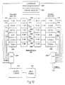
- demodulator 84 typically includes blocks, elements or modules such as arithmetic logic unit 94, a number of registers 96, at least on First-In-First-Out or FIFO memory 98, multiplexers 99, one or more finite impulse response filters 100, and one or more infinite impulse response filters 101 as well as numerous gates 102, 104 and 105 which may be NOR gates, AND gates, OR gates or any of the typical logic level devices.
- demodulator It is the purpose of the demodulator to extract carrier and timing information. How this is accomplished is in major part due to the particular type of finite impulse response filter employed.
- the combination of ALU registers, FIFO's multiplexers, and gates as well as finite impulse response and infinite impulse response filters is that which successfully demodulates the signal, with interconnection of these devices being under the control of configuration RAM 80 of Figure 5.
- FIG. 7 a typical squaring loop carrier recovery system is illustrated in which the functions performed by the low pass filter and the voltage control oscillator as well as the divide-by-two circuit, the mixer and the squaring circuit can be replicated in a single reconfigurable chip so that all of these blocks can be connected together on the fly.
- phase shifter likewise in Costas loop carrier recovery, the phase shifter, low pass filter, VCO, loop filter as well as the mixer elements are available as blocks in the demodulator which, when connected as illustrated, provides for the carrier recovery functions.
- this circuit is a typical Costas loop device for tracking the phase of a double-sided surpressed-carrier signal which is equivalent to the squarer/Phase Lock Loop System of Figure 7.
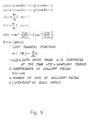
- this drawing shows an embodiment of the demodulation algorithm for demodulator 84 of Figure 5A for demodulating QPSK/QAM signals. It will be appreciated that this algorithm can be broken down into elements of blocks which form demodulator 84 in Figure 5A. However, this algorithm can also be implemented in software such that the demodulator is software-configurable. Moreover, equalizer 86, Trellis decoder 86 and R-S decoder 90 can be implemented in software and appropriately configured. Note that an advantage of the software implementation is flexibility.
- FIG. 12 a technique for detection of modulation types by the receiver involving the control of both the transmit side and the receive side and the use of modulation flags is presented.
- a transmit side 200 and a receive side 202 each having respective universal modems 204 and 206.
- a controller 208 is used to control universal modems 204 and 206 to set modulation type as illustrated at 210-220.
- Signals with the indicated modulation type are coupled to respective IF-RF stages 222.
- a video source 224 is coupled to source coding 226 which is coupled to universal modem 204 to provide source material for transmission.
- IF-RF stages 228 receive the transmission, with the received signals having formats 210-220. These signals are coupled to universal modem 206, with the decoded output placed on a bus 230, in one embodiment a 1394 bus.
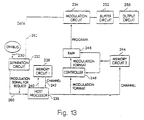
- the universal modulation of Figure 12 is one embodiment contains a separation circuit 232 coupled to modulation circuit 234 and a host processor 236.
- a Memory Circuit #1, memory 238, is coupled to host processor 236 over modulation signal line 240 and channel line 242 to provide, channel, format and frequency bandwidth.
- Host processor 236 provides channel information to Memory Circuit #2, memory 244 and format information to controller 246 and RAM 248.
- Memory Circuit #2 is coupled to controller 246 and RAM 248 to provide channel information, with RAM 248 providing a program to demodulator 250 coupled to modulation circuit 234, the output of which is buffered at 252 and outputted at 256.
- the universal modem when used in receivers, the universal modem needs to first detect the modulation type used by the incoming signals so that it can correctly choose the corresponding demodulator configurations. In one embodiment, this is done by adding modulation flag bits to the beginning of the transmitted data stream. Note that 3 bits allows up to 8 different modulation types. In what follows these bits are designated as modulation header words.
- the header is always modulated using QPSK, and it is repeated periodically during the transmission of the data signal. Therefore, it is always possible for a receiver to properly demodulate the header.
- this design requires that the above mentioned receiver configures into a QPSK demodulation mode upon power up and reconfigures itself, if necessary, after successful detection of the header word.
- the reconfigurable nature of the universal modem has the potential of improving reliability of communications by switching to a different modulator type when a predetermined noise level is detected. This is achieved in the following way.
- a channel noise detector 258 coupled to controller 208 that detects noise on the channel. Controller 208 then specifies the appropriate modulation format, frequency and bandwidth to provide more reliable communication over the channel.
- the universal modem covers VSB, QAM, QPSK, DMT, CDMA and TDMA modulations and includes the 1394 bus 230 to provide a fast protocol for video data communications and a frame of signals in the aforementioned CDMA format.
- a controller such as controller 208 controls the modulation type of universal modem 204 or 206 at both the transmitter and the receiver sides.
- each modulation type is predetermined between each transmitter and receiver.
- VSB for Channel 1 QAM for Channel 2
- QSPK for Channel 3
- DMT for Channel 4
- CDMA for Channel 5
- TDMA for Channel 6.
- Universal modem 204 at the transmitter side inputs a modulation request signal over line 260 and data signal over line 262 such as voice or image outputted from source coding 226.
- the modulation request signal and data signal are transmitted as a frame such when they are transmitted to universal modem 204 through 1394 bus 230.
- the frame signal is divided into a modulation request signal and a data signal by separation circuit 232.
- the data signal is outputted to modulation circuit 234.
- the modulation request signal is outputted to host processor 236.
- Processor 236 accesses a Memory Circuit #1 after receiving the modulation request signal.
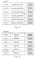
- Memory Circuit #1 has the information reflecting the modulation form for each Channel as illustrated in Figure 14, such as VSB for Channel 11, QAM for Channel 12, QSPK for channel 13, DMT for Channel 14 and TDMA for Channel 16.
- Controller 208 can change the information contained in Memory Circuit #1 freely, and gives the same order to the receiver. For example, controller 208 can increase channels, with increasing of modulation forms, or it can also change the number of a modulation form. In other words, controller 208 changes the contents of at least one memory, e.g., Memory Circuit #1, Memory Circuit #2 or any other Memory Circuit such as those associates with the receive side, it must change all of those memories. To accomplish this, processor 236 outputs a modulation format to controller 246. The frequency and the bandwidth for each channel are memorized in advance, as shown in Figure 15. Note, one can change the content of all memories in accordance with the output from controller 208. When controller 208 changes, it also conveys these changes to the memory in universal modem 206 of the receiver. For example, the frequency can be established to be 25 MHz and the bandwidth 10 Khz, with CDMA being the modulation type.
- controller 246 transmits a modulation format to RAM 248.
- RAM 248 has a program to configure modulation circuit 234 for every modulation form, e.g., VSB, QAM, QPSK, DMT, CDMA, TDMA, or other modulation type.
- controller 246 calls the program for the modulation circuit for the particular modulation format selected and outputs this format to DEMOD unit 250.
- RAM 240 configures a modulation logic circuit in demodulator 250 according to the modulation frequency information and the program. The modulation logic circuit above is then coupled to a modulation circuit 234/.
- a typical TDMA modulation logic circuit 270 is shown in Figure 16 as an example.
- Circuit 270 modulates an input data signal 272 divided by the separation associated with the modulation logic circuit of DEMOD unit 250 and the modulation frequency information from Memory Circuit #2. This is accomplished by coupling the input data signal to two filter circuits 274 and 276 respectively. The outputs of filters 274 and 276 are mixed at 278 and 280 respectively with a phase shifted signal from phase shifter 284, with the mixer circuit outputs added at adder 286.
- a typical CDMA modulation circuit is shown in Figure 17 as an example.
- a CDMA circuit 288 includes a Walsh encoder 289 coupled to an NOR gate 290 having its other input coupled to a pseudo noise or PN generator 291 having an output Pn u coupled to NOR gate 290 and a mobile unit address 292 is coupled.
- the output of NOR gate 290 is coupled in parallel to NOR gates 293 and 294 having their other inputs coupled respectively to pseudo noise or PN generator 295 and 296.
- a signal 297 from USEP digital baseband is coupled to an encoder 298 to an interleaver 299 coupled to Walsh encoder 289.
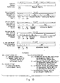
- a signal of CDMA form is shown in Figure 18 as an example of a framed signal.
- the signals from the modulator of the transmitting side are inputted to the receiving side.
- the receiver side detects the type of modulation and configures the demodulating logic circuit and outputs this for further processing.
- the demodulating is done with universal modem 206 in the receiver.
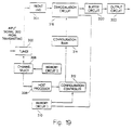
- the structure of universal modem 206 is shown in Figure 19, with the operation thereof explained hereinafter.
- an input signal 300 is coupled to a tuner 302.
- Tuner 302 couples input signal 300 to a FRONTEND unit 304.
- the functions of the FRONTEND unit are level adjustment, amplification, filtering and A/D conversion of the incoming signals from the tuner.
- the detailed description of the function of FRONTEND unit 304 is conventional and is therefore omitted.
- Tuner 302 is connected to a channel select unit 306.
- the channel select is for adjusting the tuner to the desired frequency.
- tuner 302 changes the frequency in the fixed interval according to the singals selected from 6 channels, with the interval being set in accordance with the bandwidth associated with six channels.
- tuner 302 capture the channel of incoming signals 300, the changing of the frequency is stopped and the frequency of the captured incoming signal is coupled to host processor 308.
- Channel select unit 306 inputs the frequency information stored in Memory Circuit #2 which is similar to Memory Circuit #2, 244 of Figure 13.
- the tuner searches the range of the frequency. Note that the content of Memory Circuit #2 in the receiver is the same as the content of Memory 2 in the transmitter. The content of Memory Circuit #2 in the receiver is changeable by controller 208/.
- Host processor 308 detects the demodulation type corresponding to the channel from the channel select 306, with the demodulation format being coupled to a configuration controller 312.
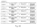
- Configuration controller 312 access memory Circuit #3 to obtain the frequency and the bandwidth, with the demodulation type, the frequency and the bandwidth subsequently coupled to RAM 314.
- Memory Circuit #3 is shown in Figure 20, with the content of Memory Circuit #3 in the receiver being changeable by the controller.
- RAM 314 stores a different kind of program for a modulation logic circuit in DEMOD unit 316 corresponding to the demodulation format, for example, VSB, QAM, QPSK, DMT, CDMA, and TDMA.
- the program for the modulation logic circuit is extracted from the RAM 314 and outputted to the DEMOD.
- DEMOD unit 316 constructs the demodulation logic circuit based on both the frequency information and the program.
- the constructed demodulation circuit 318 the output of which is coupled to buffer 320 and thence to output circuit 232.
Landscapes
- Engineering & Computer Science (AREA)
- Signal Processing (AREA)
- Computer Networks & Wireless Communication (AREA)
- Quality & Reliability (AREA)
- Digital Transmission Methods That Use Modulated Carrier Waves (AREA)
- Communication Control (AREA)
- Radio Relay Systems (AREA)
- Compression Or Coding Systems Of Tv Signals (AREA)
- Television Systems (AREA)
Abstract
Description
Claims (7)
- In a network communications system in which information is transmitted from a send side to a receive side over a communications channel, apparatus for improving system performance including means for sensing a channel parameter and for changing the modulation format of the transmitted information responsive thereto.
- The apparatus of Claim 1, wherein said means includes a universal modem at each of said sides, each universal modem providing different modulation formats for use in the modulation and demodulation of a signal, the universal modem at the transmit side including a modulator and the universal modem at the receive side including a demodulator, said modulator and demodulator each having software-configurable logic means for respectively providing modulation and demodulation of a signal,means for generating as an output configuration instructions for said software-configurable logic means;means for coupling said output to said software configurable logic means to configure said modems for the modulation format specified by said configuration instructions;means coupled to said channel for detecting said parameter; and,means responsive to the detecting of said parameter for causing said instruction generating means to change the modulation format generated by the universal modem at said send side and the demodulation format of the universal modem at said receive side to a predetermined format.
- The apparatus of Claim 2, wherein said detected parameter is channel noise, and wherein said predetermined format is one which minimizes the effects of channel noise.
- The apparatus of Claim 3, wherein said software-configurable logic means includes a number of elements, each performing a different modulation/demodulation function and means for interconnecting said elements to perform in accordance with said configuration instructions.
- The apparatus of Claim 4, wherein said elements are taken from the group consisting of arithmetic logic units, registers, fifo buffers, gates, finite impulse response filters and infinite impulse response filters.
- The apparatus of Claim 2, wherein said demodulator includes a software-configurable equalizer wherein said coupling means includes means for coupling said configuration I instructions to said equalizer.
- The apparatus of Claim 2, wherein said parameter detecting an modulation format changing means includes,means for generating a control signal for specifying modulation formats, each of said modems coupled to said control signal and providing respectively modulation and demodulatin in accordance with the format specified by said control signal;means for generating as an output different instructions for different modulation formats, said instructions including modulation format configuration data based on the modulation format specified by said control signal;a memory for storing said modulation format configuration data, said memory being coupled to an associated modem for supplying said configuration data thereto; and,means responsive to said control signal to download said modulation format configuration data from said memory to configure the associated modem for one of said different modulation formats in accordance with the associated stored configuration data.
Priority Applications (4)
| Application Number | Priority Date | Filing Date | Title |
|---|---|---|---|
| EP00122532A EP1071237A3 (en) | 1998-01-02 | 1998-12-17 | Universal modem for digital video, audio and data communications |
| EP00122530A EP1071235A3 (en) | 1998-01-02 | 1998-12-17 | Universal modem for digital video, audio and data communications |
| EP00122531A EP1071236A3 (en) | 1998-01-02 | 1998-12-17 | Universal modem for digital video, audio and data communications |
| EP00122533A EP1071238A3 (en) | 1998-01-02 | 1998-12-17 | Universal modem for digital video, audio and data communications |
Applications Claiming Priority (2)
| Application Number | Priority Date | Filing Date | Title |
|---|---|---|---|
| US2438 | 1993-01-08 | ||
| US09/002,438 US6192070B1 (en) | 1998-01-02 | 1998-01-02 | Universal modem for digital video, audio and data communications |
Related Child Applications (4)
| Application Number | Title | Priority Date | Filing Date |
|---|---|---|---|
| EP00122532A Division EP1071237A3 (en) | 1998-01-02 | 1998-12-17 | Universal modem for digital video, audio and data communications |
| EP00122530A Division EP1071235A3 (en) | 1998-01-02 | 1998-12-17 | Universal modem for digital video, audio and data communications |
| EP00122533A Division EP1071238A3 (en) | 1998-01-02 | 1998-12-17 | Universal modem for digital video, audio and data communications |
| EP00122531A Division EP1071236A3 (en) | 1998-01-02 | 1998-12-17 | Universal modem for digital video, audio and data communications |
Publications (2)
| Publication Number | Publication Date |
|---|---|
| EP0928084A2 true EP0928084A2 (en) | 1999-07-07 |
| EP0928084A3 EP0928084A3 (en) | 2001-11-21 |
Family
ID=21700762
Family Applications (5)
| Application Number | Title | Priority Date | Filing Date |
|---|---|---|---|
| EP98124048A Withdrawn EP0928084A3 (en) | 1998-01-02 | 1998-12-17 | Universal modem for digital video, audio and data communications |
| EP00122533A Withdrawn EP1071238A3 (en) | 1998-01-02 | 1998-12-17 | Universal modem for digital video, audio and data communications |
| EP00122530A Withdrawn EP1071235A3 (en) | 1998-01-02 | 1998-12-17 | Universal modem for digital video, audio and data communications |
| EP00122532A Withdrawn EP1071237A3 (en) | 1998-01-02 | 1998-12-17 | Universal modem for digital video, audio and data communications |
| EP00122531A Withdrawn EP1071236A3 (en) | 1998-01-02 | 1998-12-17 | Universal modem for digital video, audio and data communications |
Family Applications After (4)
| Application Number | Title | Priority Date | Filing Date |
|---|---|---|---|
| EP00122533A Withdrawn EP1071238A3 (en) | 1998-01-02 | 1998-12-17 | Universal modem for digital video, audio and data communications |
| EP00122530A Withdrawn EP1071235A3 (en) | 1998-01-02 | 1998-12-17 | Universal modem for digital video, audio and data communications |
| EP00122532A Withdrawn EP1071237A3 (en) | 1998-01-02 | 1998-12-17 | Universal modem for digital video, audio and data communications |
| EP00122531A Withdrawn EP1071236A3 (en) | 1998-01-02 | 1998-12-17 | Universal modem for digital video, audio and data communications |
Country Status (3)
| Country | Link |
|---|---|
| US (1) | US6192070B1 (en) |
| EP (5) | EP0928084A3 (en) |
| JP (5) | JPH11284688A (en) |
Cited By (28)
| Publication number | Priority date | Publication date | Assignee | Title |
|---|---|---|---|---|
| WO2000069086A1 (en) * | 1999-05-10 | 2000-11-16 | Sirius Communications N.V. | Method and apparatus for high-speed software reconfigurable code division multiple access communication |
| FR2799596A1 (en) * | 1999-10-11 | 2001-04-13 | Canon Kk | Equipment for optimising a multicarrier modulation transmission system, comprises one multicarrier modulator which favors a minimum error rate and a second which favors maximum information flow |
| WO2001008314A3 (en) * | 1999-07-23 | 2001-05-31 | Sirius Comm N V | Method and apparatus for high-speed software reconfigurable code division multiple access communication |
| WO2001065848A1 (en) * | 2000-03-02 | 2001-09-07 | Koninklijke Philips Electronics N.V. | System and method for improving video transmission over a wireless network. |
| WO2002017524A1 (en) * | 2000-08-25 | 2002-02-28 | Sony Corporation | Digital broadcast system |
| GB2367215A (en) * | 2000-09-25 | 2002-03-27 | Ogier Electronics Ltd | In a point to multipoint system establishing a reference frequency at the hub and transmitting it to all subscribers as a common reference |
| GB2370476A (en) * | 2000-12-22 | 2002-06-26 | Ubinetics | Combined demodulation of OFDM and CDMA signals using reduced area on an ASIC by sharing FFT hardware |
| GB2343815B (en) * | 1998-11-12 | 2003-10-22 | Sony Uk Ltd | Digital receiver |
| GB2392354A (en) * | 2002-08-23 | 2004-02-25 | Samsung Electronics Co Ltd | Integrated modulators and demodulators |
| WO2004062304A3 (en) * | 2003-01-02 | 2005-04-28 | Qualcomm Inc | Method and apparatus for broadcast services in a communication system |
| WO2005062193A2 (en) | 2003-12-15 | 2005-07-07 | Intel Corporation | Apparatus, systems, and methods for data transmission |
| US7039120B1 (en) | 1998-11-30 | 2006-05-02 | Canon Kabushiki Kaisha | Device and method for the dynamic allocation of frequencies for multicarrier modulation systems |
| US7269126B2 (en) | 1998-05-06 | 2007-09-11 | Agilent Technologies, Inc. | Method for code division multiple access communication with increased capacity through self-noise reduction |
| EP1881661A1 (en) * | 2006-07-20 | 2008-01-23 | Abilis Systems Sarl | Method and device to process a received analog signal and to extract digital data there from according to a plurality of protocols |
| US7327779B1 (en) | 1999-07-23 | 2008-02-05 | Agilent Technologies, Inc. | Method and apparatus for high-speed software reconfigurable code division multiple access communication |
| EP1244233A3 (en) * | 2001-03-22 | 2008-02-20 | Grundig Multimedia B.V. | Apparatus and method for receiving radio broadcast signals of different transmission systems |
| US7372888B1 (en) | 1999-05-10 | 2008-05-13 | Agilent Technologies Inc. | Method and apparatus for software reconfigurable communication transmission/reception and navigation signal reception |
| CN1771680B (en) * | 2003-04-08 | 2010-06-09 | 摩托罗拉公司 | method and device for transmitting and receiving data |
| US8077679B2 (en) | 2001-03-28 | 2011-12-13 | Qualcomm Incorporated | Method and apparatus for providing protocol options in a wireless communication system |
| US8098818B2 (en) | 2003-07-07 | 2012-01-17 | Qualcomm Incorporated | Secure registration for a multicast-broadcast-multimedia system (MBMS) |
| US8130781B2 (en) | 2005-02-28 | 2012-03-06 | Intellectual Ventures I Llc | Method and apparatus for providing dynamic selection of carriers |
| US8571119B2 (en) | 2011-04-01 | 2013-10-29 | Saankhya Labs Pvt. Ltd | Software defined radio for modulation and demodulation of multiple communication standards |
| US8713400B2 (en) | 2001-10-12 | 2014-04-29 | Qualcomm Incorporated | Method and system for reduction of decoding complexity in a communication system |
| US8718279B2 (en) | 2003-07-08 | 2014-05-06 | Qualcomm Incorporated | Apparatus and method for a secure broadcast system |
| US8724803B2 (en) | 2003-09-02 | 2014-05-13 | Qualcomm Incorporated | Method and apparatus for providing authenticated challenges for broadcast-multicast communications in a communication system |
| US8983065B2 (en) | 2001-10-09 | 2015-03-17 | Qualcomm Incorporated | Method and apparatus for security in a data processing system |
| CN104635513A (en) * | 2013-11-06 | 2015-05-20 | 宁夏新航信息科技有限公司 | Device and system for wireless remote measuring and control |
| US9100457B2 (en) | 2001-03-28 | 2015-08-04 | Qualcomm Incorporated | Method and apparatus for transmission framing in a wireless communication system |
Families Citing this family (128)
| Publication number | Priority date | Publication date | Assignee | Title |
|---|---|---|---|---|
| DE19737850A1 (en) * | 1997-08-29 | 1999-04-08 | Siemens Ag | Method and communication system for the synchronization of two devices on a predeterminable data transmission method |
| CA2242857A1 (en) * | 1998-07-09 | 2000-01-09 | Erik H. Boch | Combining qam and qpsk to optimize license capacity in cellular, multipoint wireless access systems |
| US7079584B2 (en) * | 1998-08-10 | 2006-07-18 | Kamilo Feher | OFDM, CDMA, spread spectrum, TDMA, cross-correlated and filtered modulation |
| US6470055B1 (en) | 1998-08-10 | 2002-10-22 | Kamilo Feher | Spectrally efficient FQPSK, FGMSK, and FQAM for enhanced performance CDMA, TDMA, GSM, OFDN, and other systems |
| US6757334B1 (en) * | 1998-08-10 | 2004-06-29 | Kamilo Feher | Bit rate agile third-generation wireless CDMA, GSM, TDMA and OFDM system |
| US7548787B2 (en) | 2005-08-03 | 2009-06-16 | Kamilo Feher | Medical diagnostic and communication system |
| US7415066B2 (en) * | 1998-08-10 | 2008-08-19 | Kamilo Feher | Mis-matched modulation-demodulation format selectable filters |
| US7593481B2 (en) * | 1998-08-31 | 2009-09-22 | Kamilo Feher | CDMA, W-CDMA, 3rd generation interoperable modem format selectable (MFS) systems with GMSK modulated systems |
| US8050345B1 (en) | 1999-08-09 | 2011-11-01 | Kamilo Feher | QAM and GMSK systems |
| EP1035660B1 (en) * | 1999-01-05 | 2008-02-27 | Motorola, Inc. | Portable communication device |
| WO2000045328A1 (en) * | 1999-01-26 | 2000-08-03 | Koninklijke Philips Electronics N.V. | Data carrier provided with at least two decoding stages |
| US6463107B1 (en) * | 1999-07-01 | 2002-10-08 | Telefonaktiebolaget Lm Ericsson (Publ) | Methods and apparatuses for synchronization and modulation type detection |
| US7260369B2 (en) * | 2005-08-03 | 2007-08-21 | Kamilo Feher | Location finder, tracker, communication and remote control system |
| US9373251B2 (en) | 1999-08-09 | 2016-06-21 | Kamilo Feher | Base station devices and automobile wireless communication systems |
| US9813270B2 (en) | 1999-08-09 | 2017-11-07 | Kamilo Feher | Heart rate sensor and medical diagnostics wireless devices |
| US9307407B1 (en) | 1999-08-09 | 2016-04-05 | Kamilo Feher | DNA and fingerprint authentication of mobile devices |
| JP2001127810A (en) * | 1999-10-28 | 2001-05-11 | Sony Corp | Modulation method recognition apparatus and method |
| US6442129B1 (en) * | 1999-12-06 | 2002-08-27 | Intellon Corporation | Enhanced channel estimation |
| US6801495B1 (en) * | 2000-02-28 | 2004-10-05 | Nortel Networks Limited | High capacity robust modem for multiple classes of services |
| EP1267508A1 (en) * | 2000-02-29 | 2002-12-18 | Fujitsu Limited | Encoding method for multicarrier transmission and encoder using the same |
| US6389359B1 (en) * | 2000-07-12 | 2002-05-14 | Links Point, Inc. | Methods for automatically detecting GPS hardware |
| US6742071B1 (en) * | 2000-07-25 | 2004-05-25 | Cypress Semiconductor Corp. | Real-time I/O processor used to implement bus interface protocols |
| US6785556B2 (en) | 2000-08-11 | 2004-08-31 | Novatel Wireless, Inc. | Method and apparatus for a software configurable wireless modem adaptable for multiple modes of operation |
| AU2001284795A1 (en) * | 2000-08-11 | 2002-02-25 | Novatel Wireless, Inc. | Method and apparatus for a software configurable wireless modem adaptable for multiple modes of operation |
| US9094226B2 (en) * | 2000-08-30 | 2015-07-28 | Broadcom Corporation | Home network system and method |
| US8724485B2 (en) * | 2000-08-30 | 2014-05-13 | Broadcom Corporation | Home network system and method |
| EP1346513B1 (en) * | 2000-08-30 | 2010-10-20 | Tmt Coaxial Networks Inc. | A home network system and method |
| FR2820564B1 (en) * | 2001-02-02 | 2003-04-18 | Nortel Networks Ltd | MODULE SIGNAL TRANSMISSION AND RECEPTION DEVICES |
| JP3881959B2 (en) * | 2001-03-05 | 2007-02-14 | 三菱電機株式会社 | Transmission format judgment method |
| US6940827B2 (en) | 2001-03-09 | 2005-09-06 | Adaptix, Inc. | Communication system using OFDM for one direction and DSSS for another direction |
| US6836839B2 (en) * | 2001-03-22 | 2004-12-28 | Quicksilver Technology, Inc. | Adaptive integrated circuitry with heterogeneous and reconfigurable matrices of diverse and adaptive computational units having fixed, application specific computational elements |
| US7752419B1 (en) | 2001-03-22 | 2010-07-06 | Qst Holdings, Llc | Method and system for managing hardware resources to implement system functions using an adaptive computing architecture |
| US7653710B2 (en) | 2002-06-25 | 2010-01-26 | Qst Holdings, Llc. | Hardware task manager |
| US7489779B2 (en) * | 2001-03-22 | 2009-02-10 | Qstholdings, Llc | Hardware implementation of the secure hash standard |
| US7249242B2 (en) | 2002-10-28 | 2007-07-24 | Nvidia Corporation | Input pipeline registers for a node in an adaptive computing engine |
| US7400668B2 (en) * | 2001-03-22 | 2008-07-15 | Qst Holdings, Llc | Method and system for implementing a system acquisition function for use with a communication device |
| US7962716B2 (en) * | 2001-03-22 | 2011-06-14 | Qst Holdings, Inc. | Adaptive integrated circuitry with heterogeneous and reconfigurable matrices of diverse and adaptive computational units having fixed, application specific computational elements |
| US7027530B2 (en) * | 2001-04-11 | 2006-04-11 | Atheros Communications, Inc. | Method and apparatus for maximizing receiver performance utilizing mid-packet gain changes |
| US8498368B1 (en) | 2001-04-11 | 2013-07-30 | Qualcomm Incorporated | Method and system for optimizing gain changes by identifying modulation type and rate |
| US6577678B2 (en) * | 2001-05-08 | 2003-06-10 | Quicksilver Technology | Method and system for reconfigurable channel coding |
| US20020184291A1 (en) * | 2001-05-31 | 2002-12-05 | Hogenauer Eugene B. | Method and system for scheduling in an adaptable computing engine |
| JP2003070056A (en) * | 2001-08-28 | 2003-03-07 | Ntt Docomo Inc | Communication channel setting method, communication control device, and wireless communication system |
| KR100800807B1 (en) * | 2001-11-20 | 2008-02-01 | 삼성전자주식회사 | Method and apparatus for determining modulation scheme of retransmission in communication system supporting retransmission |
| US7046635B2 (en) | 2001-11-28 | 2006-05-16 | Quicksilver Technology, Inc. | System for authorizing functionality in adaptable hardware devices |
| US6986021B2 (en) | 2001-11-30 | 2006-01-10 | Quick Silver Technology, Inc. | Apparatus, method, system and executable module for configuration and operation of adaptive integrated circuitry having fixed, application specific computational elements |
| US8412915B2 (en) | 2001-11-30 | 2013-04-02 | Altera Corporation | Apparatus, system and method for configuration of adaptive integrated circuitry having heterogeneous computational elements |
| US7602740B2 (en) * | 2001-12-10 | 2009-10-13 | Qst Holdings, Inc. | System for adapting device standards after manufacture |
| US7215701B2 (en) * | 2001-12-12 | 2007-05-08 | Sharad Sambhwani | Low I/O bandwidth method and system for implementing detection and identification of scrambling codes |
| US7088825B2 (en) * | 2001-12-12 | 2006-08-08 | Quicksilver Technology, Inc. | Low I/O bandwidth method and system for implementing detection and identification of scrambling codes |
| US7403981B2 (en) | 2002-01-04 | 2008-07-22 | Quicksilver Technology, Inc. | Apparatus and method for adaptive multimedia reception and transmission in communication environments |
| JP3711078B2 (en) * | 2002-02-27 | 2005-10-26 | 日本電信電話株式会社 | Multi-rate group modem, multi-rate group transmitter, receiver and transmitter / receiver |
| US7493375B2 (en) | 2002-04-29 | 2009-02-17 | Qst Holding, Llc | Storage and delivery of device features |
| US7328414B1 (en) * | 2003-05-13 | 2008-02-05 | Qst Holdings, Llc | Method and system for creating and programming an adaptive computing engine |
| US7660984B1 (en) | 2003-05-13 | 2010-02-09 | Quicksilver Technology | Method and system for achieving individualized protected space in an operating system |
| US7907669B2 (en) * | 2002-08-02 | 2011-03-15 | Omnitek Partners, Llc | Low-detectability communication between a transmitter and receiver |
| US20040037311A1 (en) * | 2002-08-07 | 2004-02-26 | Phonex Broadband Corporation | Digital narrow band power line communication system |
| US8108656B2 (en) | 2002-08-29 | 2012-01-31 | Qst Holdings, Llc | Task definition for specifying resource requirements |
| US7937591B1 (en) | 2002-10-25 | 2011-05-03 | Qst Holdings, Llc | Method and system for providing a device which can be adapted on an ongoing basis |
| US7478031B2 (en) | 2002-11-07 | 2009-01-13 | Qst Holdings, Llc | Method, system and program for developing and scheduling adaptive integrated circuity and corresponding control or configuration information |
| US8276135B2 (en) | 2002-11-07 | 2012-09-25 | Qst Holdings Llc | Profiling of software and circuit designs utilizing data operation analyses |
| US7225301B2 (en) | 2002-11-22 | 2007-05-29 | Quicksilver Technologies | External memory controller node |
| US7424039B2 (en) * | 2003-03-28 | 2008-09-09 | Nortel Networks Limited | Method and apparatus for processing multiple common frequency signals through a single cable |
| US7782827B2 (en) * | 2003-03-28 | 2010-08-24 | Nortel Networks Limited | Method and apparatus for processing multiple common frequency signals through a single cable using circulators |
| US7715350B2 (en) | 2003-06-12 | 2010-05-11 | Broadcom Corporation | Classifier for communication device |
| US7609297B2 (en) * | 2003-06-25 | 2009-10-27 | Qst Holdings, Inc. | Configurable hardware based digital imaging apparatus |
| DE10351286B4 (en) * | 2003-10-31 | 2009-12-31 | Sennheiser Electronic Gmbh & Co. Kg | Infrared headphone / hearing aid |
| US7365680B2 (en) * | 2004-02-10 | 2008-04-29 | Sirf Technology, Inc. | Location services system that reduces auto-correlation or cross-correlation in weak signals |
| US7729726B2 (en) * | 2004-03-26 | 2010-06-01 | Nortel Networks Limited | Feeder cable reduction |
| US7430263B1 (en) | 2004-05-06 | 2008-09-30 | Batzer Patricia F | System and method for timing correction for fast PN acquisition |
| US7443312B2 (en) * | 2004-06-08 | 2008-10-28 | Halliburton Energy Services, Inc. | Downhole telemetry system having discrete multi-tone modulation with QAM fallback |
| KR100621571B1 (en) * | 2004-06-25 | 2006-09-14 | 삼성전자주식회사 | Network repeater and relay method |
| US8135086B1 (en) | 2004-08-09 | 2012-03-13 | Rockstar Bidco, LP | Cable reduction |
| US7440517B1 (en) * | 2004-09-17 | 2008-10-21 | Henrie Roland R | Method and apparatus for switching between multiple waveforms |
| US7421004B2 (en) * | 2004-10-05 | 2008-09-02 | Kamilo Feher | Broadband, ultra wideband and ultra narrowband reconfigurable interoperable systems |
| US7359449B2 (en) * | 2004-10-05 | 2008-04-15 | Kamilo Feher | Data communication for wired and wireless communication |
| US20060176966A1 (en) * | 2005-02-07 | 2006-08-10 | Stewart Kenneth A | Variable cyclic prefix in mixed-mode wireless communication systems |
| US7822139B2 (en) * | 2005-03-02 | 2010-10-26 | Rohde & Schwarz Gmbh & Co. Kg | Apparatus, systems, methods and computer products for providing a virtual enhanced training sequence |
| WO2006094054A2 (en) * | 2005-03-02 | 2006-09-08 | Rohde & Schwarz Gmbh & Co.Kg | Apparatus, systems and methods for providing enhancements to atsc networks using synchronous vestigial sideband (vsb) frame slicing |
| US20060245516A1 (en) * | 2005-03-02 | 2006-11-02 | Rohde & Schwarz, Inc. | Apparatus, systems and methods for providing in-band atsc vestigial sideband signaling or out-of-band signaling |
| US20060245384A1 (en) * | 2005-05-02 | 2006-11-02 | Talukdar Anup K | Method and apparatus for transmitting data |
| JP2007013403A (en) * | 2005-06-29 | 2007-01-18 | Agilent Technol Inc | Time difference measurement method, synchronization method, measurement method, time difference measurement device, synchronization device, and measurement device |
| US7764741B2 (en) * | 2005-07-28 | 2010-07-27 | Broadcom Corporation | Modulation-type discrimination in a wireless communication network |
| US7738604B2 (en) * | 2005-07-28 | 2010-06-15 | Broadcom Corporation | Modulation-type discrimination in a wireless local area network |
| US10009956B1 (en) | 2017-09-02 | 2018-06-26 | Kamilo Feher | OFDM, 3G and 4G cellular multimode systems and wireless mobile networks |
| US7280810B2 (en) | 2005-08-03 | 2007-10-09 | Kamilo Feher | Multimode communication system |
| US8009605B1 (en) * | 2005-08-08 | 2011-08-30 | Rockwell Collins, Inc. | Low power, programmable modem for software defined radio applications |
| US8452333B2 (en) * | 2005-12-12 | 2013-05-28 | Apple Inc. | Feeder cable reduction |
| JP4674190B2 (en) * | 2006-07-13 | 2011-04-20 | Okiセミコンダクタ株式会社 | Multimode receiver circuit |
| US8400998B2 (en) | 2006-08-23 | 2013-03-19 | Motorola Mobility Llc | Downlink control channel signaling in wireless communication systems |
| US7782850B2 (en) | 2006-11-20 | 2010-08-24 | Broadcom Corporation | MAC to PHY interface apparatus and methods for transmission of packets through a communications network |
| US7742495B2 (en) * | 2006-11-20 | 2010-06-22 | Broadcom Corporation | System and method for retransmitting packets over a network of communication channels |
| US8090043B2 (en) | 2006-11-20 | 2012-01-03 | Broadcom Corporation | Apparatus and methods for compensating for signal imbalance in a receiver |
| MX2009007049A (en) | 2007-02-01 | 2009-08-13 | Rohde & Schwarz | Systems, apparatus, methods and computer program products for providing atsc interoperability. |
| KR100907705B1 (en) | 2007-04-02 | 2009-07-14 | (주)디티브이인터랙티브 | IF signal generator and modulation device of digital broadcasting signal generator |
| US8345553B2 (en) | 2007-05-31 | 2013-01-01 | Broadcom Corporation | Apparatus and methods for reduction of transmission delay in a communication network |
| DE102008017290A1 (en) * | 2007-12-11 | 2009-06-18 | Rohde & Schwarz Gmbh & Co. Kg | Method and device for forming a common data stream, in particular according to the ATSC standard |
| DE102007059959B4 (en) * | 2007-12-12 | 2020-01-02 | Rohde & Schwarz Gmbh & Co. Kg | Method and system for transmitting data between a central radio station and at least one transmitter |
| DE102008056703A1 (en) * | 2008-07-04 | 2010-01-07 | Rohde & Schwarz Gmbh & Co. Kg | Method and system for time synchronization between a central office and multiple transmitters |
| US8355458B2 (en) | 2008-06-25 | 2013-01-15 | Rohde & Schwarz Gmbh & Co. Kg | Apparatus, systems, methods and computer program products for producing a single frequency network for ATSC mobile / handheld services |
| US9112717B2 (en) | 2008-07-31 | 2015-08-18 | Broadcom Corporation | Systems and methods for providing a MoCA power management strategy |
| DE102008059028B4 (en) * | 2008-10-02 | 2021-12-02 | Rohde & Schwarz GmbH & Co. Kommanditgesellschaft | Method and device for generating a transport data stream with image data |
| MX2011004645A (en) * | 2008-11-06 | 2011-05-30 | Rohde & Schwarz | Method and system for synchronized mapping of data packets in an atsc data stream. |
| US8254413B2 (en) * | 2008-12-22 | 2012-08-28 | Broadcom Corporation | Systems and methods for physical layer (“PHY”) concatenation in a multimedia over coax alliance network |
| US8238227B2 (en) | 2008-12-22 | 2012-08-07 | Broadcom Corporation | Systems and methods for providing a MoCA improved performance for short burst packets |
| US8213309B2 (en) * | 2008-12-22 | 2012-07-03 | Broadcom Corporation | Systems and methods for reducing latency and reservation request overhead in a communications network |
| US20100238932A1 (en) * | 2009-03-19 | 2010-09-23 | Broadcom Corporation | Method and apparatus for enhanced packet aggregation |
| US8982745B2 (en) * | 2009-03-21 | 2015-03-17 | Rohde & Schwarz Gmbh & Co. Kg | Method for improving the data rate of mobile/handheld data and the quality of channel estimation in an ATSC-M/H transport data stream |
| US8553547B2 (en) * | 2009-03-30 | 2013-10-08 | Broadcom Corporation | Systems and methods for retransmitting packets over a network of communication channels |
| US20100254278A1 (en) | 2009-04-07 | 2010-10-07 | Broadcom Corporation | Assessment in an information network |
| DE102009025219A1 (en) * | 2009-04-07 | 2010-10-14 | Rohde & Schwarz Gmbh & Co. Kg | Method and device for continuously adapting coding parameters to a variable payload data rate |
| US8730798B2 (en) * | 2009-05-05 | 2014-05-20 | Broadcom Corporation | Transmitter channel throughput in an information network |
| US8867355B2 (en) | 2009-07-14 | 2014-10-21 | Broadcom Corporation | MoCA multicast handling |
| US8537004B2 (en) * | 2009-09-30 | 2013-09-17 | Carefusion 303, Inc. | Verification of dispensed items |
| US8942250B2 (en) | 2009-10-07 | 2015-01-27 | Broadcom Corporation | Systems and methods for providing service (“SRV”) node selection |
| DE102009057363B4 (en) | 2009-10-16 | 2013-04-18 | Rohde & Schwarz Gmbh & Co. Kg | Method and device for the efficient transmission of nationwide and regionally broadcast program and service data |
| JP5990466B2 (en) | 2010-01-21 | 2016-09-14 | スビラル・インコーポレーテッド | Method and apparatus for a general purpose multi-core system for implementing stream-based operations |
| US8611327B2 (en) | 2010-02-22 | 2013-12-17 | Broadcom Corporation | Method and apparatus for policing a QoS flow in a MoCA 2.0 network |
| US8514860B2 (en) * | 2010-02-23 | 2013-08-20 | Broadcom Corporation | Systems and methods for implementing a high throughput mode for a MoCA device |
| US8989021B2 (en) | 2011-01-20 | 2015-03-24 | Rohde & Schwarz Gmbh & Co. Kg | Universal broadband broadcasting |
| US8948596B2 (en) | 2011-07-01 | 2015-02-03 | CetusView Technologies, LLC | Neighborhood node mapping methods and apparatus for ingress mitigation in cable communication systems |
| GB2496164B (en) * | 2011-11-03 | 2014-01-01 | Renesas Mobile Corp | Method and apparatus for radio receiver equalization |
| CN103595673B (en) * | 2012-06-16 | 2017-04-19 | 天地融科技股份有限公司 | Audio data transmission method |
| CN103595672B (en) * | 2012-06-16 | 2017-06-06 | 天地融科技股份有限公司 | Audio data transmission method |
| CN102769591B (en) * | 2012-06-21 | 2015-04-08 | 天地融科技股份有限公司 | Self-adaptive method, self-adaptive system and self-adaptive device for audio communication modulation modes and electronic signature implement |
| US9615401B2 (en) | 2012-12-11 | 2017-04-04 | Qualcomm Incorporated | Methods and apparatus for updating a device configuration |
| GB2529092A (en) | 2013-03-15 | 2016-02-10 | Certusview Technologies Llc | Electro-optical apparatus and methods for upstream alignment of cable communication systems |
| CN109889365B (en) * | 2019-01-04 | 2022-02-01 | 烽火通信科技股份有限公司 | OTN transmission method based on modulation mode switching |
| CN114650077B (en) * | 2020-12-17 | 2023-07-14 | 航天科工惯性技术有限公司 | Communication circuit for sending and receiving self-controlled RS485 interface |
Family Cites Families (24)
| Publication number | Priority date | Publication date | Assignee | Title |
|---|---|---|---|---|
| JPS5963845A (en) * | 1982-10-01 | 1984-04-11 | Matsushita Graphic Commun Syst Inc | Controlling method of transmission |
| US4679227A (en) * | 1985-05-20 | 1987-07-07 | Telebit Corporation | Ensemble modem structure for imperfect transmission media |
| JP2906462B2 (en) * | 1989-07-18 | 1999-06-21 | ソニー株式会社 | Television receiver |
| US5040192A (en) * | 1990-02-06 | 1991-08-13 | Hayes Microcomputer Products, Inc. | Method and apparatus for optimally autocorrelating an FSK signal |
| US5289476A (en) * | 1991-05-10 | 1994-02-22 | Echelon Corporation | Transmission mode detection in a modulated communication system |
| JP3193378B2 (en) * | 1991-06-03 | 2001-07-30 | ブリテイッシュ・テレコミュニケーションズ・パブリック・リミテッド・カンパニー | QAM system in which constellation is changed according to channel quality |
| US5331672A (en) * | 1991-07-09 | 1994-07-19 | General Datacomm, Inc. | Automatic detector and selector of RS-232 or V.35 interface |
| JP2776094B2 (en) * | 1991-10-31 | 1998-07-16 | 日本電気株式会社 | Variable modulation communication method |
| US5249218A (en) * | 1992-04-06 | 1993-09-28 | Spectrum Information Technologies, Inc. | Programmable universal interface system |
| WO1994011955A1 (en) * | 1992-11-06 | 1994-05-26 | Pericle Communications Company | Adaptive data rate modem |
| JPH06343085A (en) * | 1993-04-07 | 1994-12-13 | Hitachi Ltd | Method and device for signal decoding demodulation |
| JPH0775099A (en) * | 1993-05-07 | 1995-03-17 | Philips Electron Nv | Multiplex quadrature amplitude modulation television transmission system, transmitter and receiver |
| US5764699A (en) * | 1994-03-31 | 1998-06-09 | Motorola, Inc. | Method and apparatus for providing adaptive modulation in a radio communication system |
| US5533004A (en) * | 1994-11-07 | 1996-07-02 | Motorola, Inc. | Method for providing and selecting amongst multiple data rates in a time division multiplexed system |
| US5550881A (en) * | 1995-04-13 | 1996-08-27 | Motorola, Inc. | Automatic modulation mode selecting unit and method for modems |
| US5671253A (en) * | 1995-07-12 | 1997-09-23 | Thomson Consumer Electronics, Inc. | Apparatus for demodulating and decoding video signals encoded in different formats |
| US6442145B1 (en) * | 1996-01-03 | 2002-08-27 | International Business Machines Corporation | Robust method and apparatus enabling multi-mode wireless optical communication |
| US5706428A (en) * | 1996-03-14 | 1998-01-06 | Lucent Technologies Inc. | Multirate wireless data communication system |
| WO1997048191A1 (en) * | 1996-06-13 | 1997-12-18 | Broadband Networks Inc. | Wide-area wireless distribution system |
| US6366326B1 (en) * | 1996-08-01 | 2002-04-02 | Thomson Consumer Electronics Inc. | System for acquiring, processing, and storing video data and program guides transmitted in different coding formats |
| US5982819A (en) * | 1996-09-23 | 1999-11-09 | Motorola, Inc. | Modulation format adaptive messaging receiver and method thereof |
| US5940438A (en) * | 1997-02-18 | 1999-08-17 | Mitsubishi Electric Information Technology Center America, Inc (Ita) | Universal modem for digital video, audio and data communications |
| US5982807A (en) * | 1997-03-17 | 1999-11-09 | Harris Corporation | High data rate spread spectrum transceiver and associated methods |
| US5991337A (en) * | 1997-11-24 | 1999-11-23 | 3Com Corporation | Method and apparatus for improving the signal-to-noise ratio of low-magnitude input signals in modems |
-
1998
- 1998-01-02 US US09/002,438 patent/US6192070B1/en not_active Expired - Fee Related
- 1998-12-17 EP EP98124048A patent/EP0928084A3/en not_active Withdrawn
- 1998-12-17 EP EP00122533A patent/EP1071238A3/en not_active Withdrawn
- 1998-12-17 EP EP00122530A patent/EP1071235A3/en not_active Withdrawn
- 1998-12-17 EP EP00122532A patent/EP1071237A3/en not_active Withdrawn
- 1998-12-17 EP EP00122531A patent/EP1071236A3/en not_active Withdrawn
- 1998-12-28 JP JP10373317A patent/JPH11284688A/en active Pending
-
2000
- 2000-05-26 JP JP2000156914A patent/JP2001007888A/en active Pending
- 2000-05-26 JP JP2000156913A patent/JP2001007883A/en active Pending
- 2000-05-26 JP JP2000156916A patent/JP2001007881A/en active Pending
- 2000-05-26 JP JP2000156915A patent/JP2001036598A/en not_active Abandoned
Cited By (40)
| Publication number | Priority date | Publication date | Assignee | Title |
|---|---|---|---|---|
| US7269126B2 (en) | 1998-05-06 | 2007-09-11 | Agilent Technologies, Inc. | Method for code division multiple access communication with increased capacity through self-noise reduction |
| GB2343815B (en) * | 1998-11-12 | 2003-10-22 | Sony Uk Ltd | Digital receiver |
| US7039120B1 (en) | 1998-11-30 | 2006-05-02 | Canon Kabushiki Kaisha | Device and method for the dynamic allocation of frequencies for multicarrier modulation systems |
| US7372888B1 (en) | 1999-05-10 | 2008-05-13 | Agilent Technologies Inc. | Method and apparatus for software reconfigurable communication transmission/reception and navigation signal reception |
| US7386005B2 (en) | 1999-05-10 | 2008-06-10 | Agilent Technologies Inc. | Method and system for high-speed software reconfigurable code division multiple access communication |
| WO2000069086A1 (en) * | 1999-05-10 | 2000-11-16 | Sirius Communications N.V. | Method and apparatus for high-speed software reconfigurable code division multiple access communication |
| US7327779B1 (en) | 1999-07-23 | 2008-02-05 | Agilent Technologies, Inc. | Method and apparatus for high-speed software reconfigurable code division multiple access communication |
| WO2001008314A3 (en) * | 1999-07-23 | 2001-05-31 | Sirius Comm N V | Method and apparatus for high-speed software reconfigurable code division multiple access communication |
| FR2799596A1 (en) * | 1999-10-11 | 2001-04-13 | Canon Kk | Equipment for optimising a multicarrier modulation transmission system, comprises one multicarrier modulator which favors a minimum error rate and a second which favors maximum information flow |
| WO2001065848A1 (en) * | 2000-03-02 | 2001-09-07 | Koninklijke Philips Electronics N.V. | System and method for improving video transmission over a wireless network. |
| US6798838B1 (en) | 2000-03-02 | 2004-09-28 | Koninklijke Philips Electronics N.V. | System and method for improving video transmission over a wireless network |
| US7697411B2 (en) | 2000-08-25 | 2010-04-13 | Sony Corporation | OFDM broadcast system for transporting streams of data |
| AU784822B2 (en) * | 2000-08-25 | 2006-06-29 | Sony Corporation | Digital broadcast system |
| WO2002017524A1 (en) * | 2000-08-25 | 2002-02-28 | Sony Corporation | Digital broadcast system |
| GB2367215A (en) * | 2000-09-25 | 2002-03-27 | Ogier Electronics Ltd | In a point to multipoint system establishing a reference frequency at the hub and transmitting it to all subscribers as a common reference |
| GB2370476A (en) * | 2000-12-22 | 2002-06-26 | Ubinetics | Combined demodulation of OFDM and CDMA signals using reduced area on an ASIC by sharing FFT hardware |
| EP1244233A3 (en) * | 2001-03-22 | 2008-02-20 | Grundig Multimedia B.V. | Apparatus and method for receiving radio broadcast signals of different transmission systems |
| US9100457B2 (en) | 2001-03-28 | 2015-08-04 | Qualcomm Incorporated | Method and apparatus for transmission framing in a wireless communication system |
| US8077679B2 (en) | 2001-03-28 | 2011-12-13 | Qualcomm Incorporated | Method and apparatus for providing protocol options in a wireless communication system |
| US8983065B2 (en) | 2001-10-09 | 2015-03-17 | Qualcomm Incorporated | Method and apparatus for security in a data processing system |
| US8713400B2 (en) | 2001-10-12 | 2014-04-29 | Qualcomm Incorporated | Method and system for reduction of decoding complexity in a communication system |
| US8730999B2 (en) | 2001-10-12 | 2014-05-20 | Qualcomm Incorporated | Method and system for reduction of decoding complexity in a communication system |
| GB2392354B (en) * | 2002-08-23 | 2006-02-01 | Samsung Electronics Co Ltd | Integrated modulators and demodulators |
| GB2392354A (en) * | 2002-08-23 | 2004-02-25 | Samsung Electronics Co Ltd | Integrated modulators and demodulators |
| WO2004062304A3 (en) * | 2003-01-02 | 2005-04-28 | Qualcomm Inc | Method and apparatus for broadcast services in a communication system |
| US7599655B2 (en) | 2003-01-02 | 2009-10-06 | Qualcomm Incorporated | Method and apparatus for broadcast services in a communication system |
| CN1771680B (en) * | 2003-04-08 | 2010-06-09 | 摩托罗拉公司 | method and device for transmitting and receiving data |
| US8098818B2 (en) | 2003-07-07 | 2012-01-17 | Qualcomm Incorporated | Secure registration for a multicast-broadcast-multimedia system (MBMS) |
| US8718279B2 (en) | 2003-07-08 | 2014-05-06 | Qualcomm Incorporated | Apparatus and method for a secure broadcast system |
| US8724803B2 (en) | 2003-09-02 | 2014-05-13 | Qualcomm Incorporated | Method and apparatus for providing authenticated challenges for broadcast-multicast communications in a communication system |
| US8243753B2 (en) | 2003-12-15 | 2012-08-14 | Intel Corporation | Data definition apparatus, systems, and methods |
| US8605746B2 (en) | 2003-12-15 | 2013-12-10 | Intel Corporation | Data definition apparatus, systems, and methods |
| US7583694B2 (en) | 2003-12-15 | 2009-09-01 | Intel Corporation | Data definition apparatus, systems, and methods |
| WO2005062193A3 (en) * | 2003-12-15 | 2005-09-29 | Intel Corp | Apparatus, systems, and methods for data transmission |
| WO2005062193A2 (en) | 2003-12-15 | 2005-07-07 | Intel Corporation | Apparatus, systems, and methods for data transmission |
| US8130781B2 (en) | 2005-02-28 | 2012-03-06 | Intellectual Ventures I Llc | Method and apparatus for providing dynamic selection of carriers |
| WO2008009595A1 (en) * | 2006-07-20 | 2008-01-24 | Abilis Systems Sarl | Method and device to process a received analog signal and to extract digital data therefrom according to a plurality of protocols |
| EP1881661A1 (en) * | 2006-07-20 | 2008-01-23 | Abilis Systems Sarl | Method and device to process a received analog signal and to extract digital data there from according to a plurality of protocols |
| US8571119B2 (en) | 2011-04-01 | 2013-10-29 | Saankhya Labs Pvt. Ltd | Software defined radio for modulation and demodulation of multiple communication standards |
| CN104635513A (en) * | 2013-11-06 | 2015-05-20 | 宁夏新航信息科技有限公司 | Device and system for wireless remote measuring and control |
Also Published As
| Publication number | Publication date |
|---|---|
| JP2001007888A (en) | 2001-01-12 |
| EP1071236A3 (en) | 2002-10-23 |
| EP1071237A2 (en) | 2001-01-24 |
| JPH11284688A (en) | 1999-10-15 |
| EP1071238A2 (en) | 2001-01-24 |
| EP1071237A3 (en) | 2002-05-02 |
| JP2001007881A (en) | 2001-01-12 |
| EP1071235A2 (en) | 2001-01-24 |
| EP0928084A3 (en) | 2001-11-21 |
| EP1071235A3 (en) | 2002-10-23 |
| US6192070B1 (en) | 2001-02-20 |
| EP1071236A2 (en) | 2001-01-24 |
| EP1071238A3 (en) | 2001-11-14 |
| JP2001036598A (en) | 2001-02-09 |
| JP2001007883A (en) | 2001-01-12 |
Similar Documents
| Publication | Publication Date | Title |
|---|---|---|
| US6192070B1 (en) | Universal modem for digital video, audio and data communications | |
| US5940438A (en) | Universal modem for digital video, audio and data communications | |
| CA2344117C (en) | Method and system for tiered digital television terrestrial broadcasting services using multi-bit-stream frequency interleaved ofdm | |
| US7653415B2 (en) | Method and system for increasing data rate in a mobile terminal using spatial multiplexing for DVB-H communication | |
| EP2254299B1 (en) | OFDM reception device | |
| CN101325471B (en) | Method and apparatus for transmitting multimedia data | |
| KR100497478B1 (en) | Method for acquiring data transmitted on a transmission channel | |
| US8027704B2 (en) | Method and system for increasing data rate in a mobile terminal using spatial multiplexing for DVB-H communication | |
| US8670372B2 (en) | System and method for scheduling and transferring data through a transmission system | |
| JPH1032557A (en) | Relay system, transmission device and relay device used for the same | |
| US8520756B2 (en) | PHY sub-channel processing | |
| US7346074B2 (en) | Communication system, signal receiving device, signal transmitting device, and communication method | |
| US7440517B1 (en) | Method and apparatus for switching between multiple waveforms | |
| JPH08265295A (en) | Orthogonal frequency division multiplex transmission system and transmitter and receiver thereof | |
| JP2004015494A (en) | Hierarchy modulation broadcast receiving system and method therefor | |
| CN1359204A (en) | Stereo data broadcasting system | |
| KR100665532B1 (en) | Terrestrial and cable composite broadcasting receiver and method | |
| KR100786400B1 (en) | DMX Receiver Reduces Channel Change Time | |
| MXPA97005810A (en) | System to receive variable coding formats and number of transmis channels | |
| MXPA97005811A (en) | System for acquiring and processing video data and program guides transmitted in different coding formats |
Legal Events
| Date | Code | Title | Description |
|---|---|---|---|
| PUAI | Public reference made under article 153(3) epc to a published international application that has entered the european phase |
Free format text: ORIGINAL CODE: 0009012 |
|
| AK | Designated contracting states |
Kind code of ref document: A2 Designated state(s): AT BE CH CY DE DK ES FI FR GB GR IE IT LI LU MC NL PT SE Kind code of ref document: A2 Designated state(s): DE FI FR GB NL |
|
| AX | Request for extension of the european patent |
Free format text: AL;LT;LV;MK;RO;SI |
|
| PUAL | Search report despatched |
Free format text: ORIGINAL CODE: 0009013 |
|
| AK | Designated contracting states |
Kind code of ref document: A3 Designated state(s): AT BE CH CY DE DK ES FI FR GB GR IE IT LI LU MC NL PT SE |
|
| 17P | Request for examination filed |
Effective date: 20020122 |
|
| 17Q | First examination report despatched |
Effective date: 20020517 |
|
| AKX | Designation fees paid |
Free format text: DE FI FR GB NL |
|
| STAA | Information on the status of an ep patent application or granted ep patent |
Free format text: STATUS: THE APPLICATION HAS BEEN WITHDRAWN |
|
| 18W | Application withdrawn |
Effective date: 20040105 |