EP0928065B1 - Multiported register file for coefficient use in filters - Google Patents
Multiported register file for coefficient use in filters Download PDFInfo
- Publication number
- EP0928065B1 EP0928065B1 EP98309987A EP98309987A EP0928065B1 EP 0928065 B1 EP0928065 B1 EP 0928065B1 EP 98309987 A EP98309987 A EP 98309987A EP 98309987 A EP98309987 A EP 98309987A EP 0928065 B1 EP0928065 B1 EP 0928065B1
- Authority
- EP
- European Patent Office
- Prior art keywords
- latch
- register file
- memory
- computation
- coefficient value
- Prior art date
- Legal status (The legal status is an assumption and is not a legal conclusion. Google has not performed a legal analysis and makes no representation as to the accuracy of the status listed.)
- Expired - Lifetime
Links
Images
Classifications
-
- H—ELECTRICITY
- H03—ELECTRONIC CIRCUITRY
- H03H—IMPEDANCE NETWORKS, e.g. RESONANT CIRCUITS; RESONATORS
- H03H21/00—Adaptive networks
- H03H21/0012—Digital adaptive filters
-
- H—ELECTRICITY
- H03—ELECTRONIC CIRCUITRY
- H03H—IMPEDANCE NETWORKS, e.g. RESONANT CIRCUITS; RESONATORS
- H03H17/00—Networks using digital techniques
- H03H17/02—Frequency selective networks
- H03H17/0223—Computation saving measures; Accelerating measures
- H03H17/0227—Measures concerning the coefficients
-
- H—ELECTRICITY
- H03—ELECTRONIC CIRCUITRY
- H03H—IMPEDANCE NETWORKS, e.g. RESONANT CIRCUITS; RESONATORS
- H03H17/00—Networks using digital techniques
- H03H17/02—Frequency selective networks
- H03H17/0248—Filters characterised by a particular frequency response or filtering method
- H03H17/0264—Filter sets with mutual related characteristics
- H03H17/0266—Filter banks
- H03H17/0269—Filter banks comprising recursive filters
Definitions
- This invention relates to multiported register files, and to methods of using a multiported register file in connection with an adaptive FIR filter.
- Prior art adaptive finite impulse response (FIR) filters employ fixed delay lines for recirculating the coefficients. Such delay lines are implemented using a series of edge triggered flip flops. As a result, in operation, the prior art delay lines consume more power than is desirable.
- FIR finite impulse response
- multiported register files are employed to implement the coefficient storage and to provide the delays in the coefficients that are necessary for filter operation.
- a multiported register file is a memory, typically small, e.g., having a capacity for four words, with at least one read port and one write port. Data written into the multiported register file may be read out therefrom in any desired order.
- the multiported register file may have additional output ports from which the data stored therein may be read out, also in any desired order, and independent from the order of any other output port.
- each multiported register file feeds data from one output port to the multiply-add portion of its associated stage of the FIR filter.
- each multiported register file feeds data from another output to the update unit for that coefficient. Note that these output ports may be the same, and if not, the data supplied to them may be the same. For coefficient use, there is no need to operate the multiported register file in the lookthrough mode described in the copending application.
- an update unit which computes new coefficient values.
- Such an update unit incorporates, or is associated with, an overflow/underflow detection and/or saturation unit, which is used in the prevention of catastrophic errors in the filter that could occur when overflow or underflow takes place.
- Such errors can occur because of the nature of conventional techniques for performing arithmetic using binary numbers. For example, when two large positive numbers represented using two's complement representation are added the result could appear to be a negative number, which clearly is erroneous.
- An overflow/underflow detection unit and/or saturation prevents this problem by supplying as an output, depending upon its incarnation, one of the following: a) flags indicating whether overflow or underflow has occurred; b) a value representing the maximum positive or negative number that can be represented as a saturation value; or c) the actual result of the calculation.
- This overflow/underflow detection and/or saturation unit lies in the critical path of coefficient updating circuitry, i.e., it is in the path that determines the maximum speed at which the updating can be performed. Thus, the speed at which the overflow/underflow detection and/or saturation process can be performed limits the speed of the updating process.
- Patent Abstracts of Japan shows a use of a multiport memory in a digital filter.
- multiported register files may be used for storing coefficients in adaptive FIR filters.
- the multiported register files of the prior copending application are improved by incorporating therein computational ability, e.g., the ability to perform computation on coefficient values or derivatives thereof, or to control the operations performed thereon.
- the multiported register file incorporates therein an overflow/underflow detection and/or saturation unit
- the multiported register file incorporates therein a special encoder which is used to speed up the multiplication process, e.g., the so-called "Booth" encoder.
- the multiported register file incorporates therein a converter for changing the representation of the coefficients e.g., a two's complement to sign-magnitude converter.
- All computation performed in the multiported register file may be performed outside of the critical path of the filtering or of the coefficient updating.
- adaptive FIR filters can be constructed which operate faster, and with lower power consumption, than those of the prior copending application.
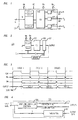
- FIG. 1 shows an exemplary multiported register file which may be used to store coefficients in a stage of a finite impulse response filter (FIR).
- FIR finite impulse response filter
- a multiported register file is a memory, typically small, e.g., having a capacity for four words, with at least one read port and one write port. Data written into the multiported register file may be read out therefrom in any desired order.
- the multiported register file may have additional output ports from which the data stored therein may be read out, also in any desired order, and independent from the order of any other output port.
- FIG. 1 shows multiported register file 101, including memory 103, which has memory locations 103-1 through 103-H, computation unit 105, and latches 107, including latches 107-1 through 107-K.
- the number of memory locations in the multiported register file is typically a small number, e.g., 4. Having a small value of H allows efficient FIR filter implementation-compared with other alternatives for implementing FIR filters-for processing signals having a sample rate that is within an order of magnitude of the fastest clock frequencies in the system, such as is found in modems for use in broadband access.
- Data is written to multiported register file 101 via write port W, which includes N data lines.
- the particular one of memory locations 103 to which data presented at write port W is written to is specified by write address port WA.
- Data is read from multiported register file 101 via any of read ports R, including read ports R 1 through R k .
- Each of read ports R 1 through R k includes a respective number of data lines M 1 through M k . If desired, a less precise representation of a value stored in multiported register file 101 may be read out therefrom.
- the particular one of memory locations 103 from which data is read for presentation to any one of read ports R 1 through R k is specified by an address supplied to the corresponding, e.g., like numbered, one of read address ports RA 1 through RA k . No read enable signal is necessary to cause an output to appear at any of read ports R 1 through R k . Simply supplying the appropriate read address is sufficient to generate the corresponding output.
- write address WA, and read address RA 1 through RA k have the same number of address lines, L.
- When and whether data is written to multiported register file 101 is a function of the value of write enable signal WE.
- WE has a first value data is written to multiported register file 101.
- WE has the complementary value of the first value data is not written to multiported register file 101.
- Data may be written to and read from multiported register file 101 at the same time. More specifically, data may be written to and read from the same particular one of memory locations 103 at the same time. Thus, a first value may be written to a particular one of memory locations 103 while at the same time a different value may be read from that very same particular location and supplied to one, or more, of read ports R 1 through R k .
- Latches 107 are conventional level sensitive latches such as are described by N. Weste and K. Eshraghian on pages 19-21 of Principles of CMOS VLSI Design, 2 nd Ed., Addison Wesley, 1992. Thus, any one of memory locations 103 may act as a master latch while any one of latches 107 may act as a slave latch to form an edge triggered flip-flop, with computation unit 105 interposed therebetween.
- FIG. 2 shows a simplified view of multiported register file 101, where only two memory locations 103 are shown with only a single read port and a single write port. Also shown is the clock signal (CLK) which is used to control operation and data transfer between memory 103 and latches 107 and coefficient update unit 109.
- CLK clock signal
- memory 103 is positive level sensitive while latch 107 is negative level sensitive. Together they form a negative edge triggered flip-flop.
- Computation unit 105 takes at least one coefficient value and performs some type of transformation on it, or passes the coefficient value unchanged. Computation unit 105 is interposed between memory locations 103 and latches 107, so that computation unit 105 may a) receive coefficient values from memory locations 103 and b) supply its output to one or more of latches 107. All computation performed in the multiported register file is performed outside of the critical path of the filtering or of the coefficient updating.
- Computation unit 105 is outside of the critical path of the filtering or of the coefficient updating because it performs its function in the so-called "dead time" between the time that the master latch, which herein is the currently addressed location in memory 103, contains the stored information and the time that the slave latch, herein latch 107, latches the information from the master latch. This is made possible because the read address signal is supplied to read address ports RA 1 through RA k earlier than the clock signal is supplied to latches 107.
- FIG. 3 shows a timing diagram for the operation of the simplified view of multiported register file 101 shown in FIG. 2.
- FIG. 3 shows signals CLK, RA, WA and OUTPUT from latch 107. Note that signals CLK, RA, and WA are supplied to multiported register file 101, which generates signal OUTPUT.
- Read address signal RA is supplied to multiported register file 101 one half cycle ahead of write address signal WA.
- signal RA which changes shortly after every positive edge of CLK, data comes out of memory 103 and is processed by computation unit 105 prior to the negative edge of CLK. Note that by shortly it is meant that there is enough time for computation unit 105 to perform its required calculation.
- latch 107 latches the processed data supplied as the output of computation unit 105. This data is then made available as OUTPUT, the output of multiported register file 101. This data is supplied to update unit 109, as well as to the multiplier of the filter (not shown) which is being implemented using multiported register file 101. Shortly after the next positive edge, RA changes and another coefficient is read out from one of memory locations 103. Meanwhile, the output data that was latched on the previous negative edge is still available from latch 107. On the next negative edge of CLK, the updated data which is supplied as the output of update unit 109 is written back into memory 103 to a location specified by WA, which changes only a short time after the negative edge of CLK.
- computation unit 105 is an overflow/underflow detection and/or saturation unit.
- FIG. 4 shows an exemplary embodiment in which computation unit 105 is implemented as overflow/underflow detection and/or saturation unit 211.
- Overflow/underflow saturation unit 211 includes overflow/underflow detection unit 501 connected to saturation detection unit 601.
- Overflow/underflow detection unit 501 may operate, for example, in a conventional, well known manner, such as by determining whether a received input a number with G bits of precision can be represented with Y bits of precision, where Y is less than G. If the received input is a number with G bits of precision and that input can be represented with Y bits of precision, no underflow or overflow is determined to occur. Therefore, the value of the input number is supplied as the output of overflow/underflow detection and/or saturation unit 211 but using only Y bits of precision. Otherwise, if the magnitude of the number is too large to be represented with only Y bits of precision, underflow, or overflow, is determined to have occurred. If overflow or underflow has occurred, the corresponding flag is set and supplied as an output. Which of overflow or underflow has occurred is determined by whether or not the input is greater than the maximum value that can be represented with Y bits of precision or less than the minimum value that can be represented with Y bits of precision.
- Saturation detection unit 601 may operate, for example, in a conventional, well known manner. For example, saturation detection unit 601 receives as inputs a number with Y bits of precision, and the values of an overflow flag and an underflow flag. If the overflow flag is set, saturation detection unit 601 supplies as an output the maximum value that can be represented using Y bits of precision. If the underflow flag is set, saturation detection unit 601 supplies as an output the minimum value that can be represented using Y bits of precision. If neither the overflow flag nor the underflow flag is set, saturation detection unit 601 supplies as an output the input value, but only using Y bits of precision.
- overflow/underflow detection and/or saturation unit 211 receives as an input a number with G bits of precision and supplies as an output a) the actual value of G using Y bits of precision, where Y is less than G, when G can be represented with Y bits of precision, or b) the maximum or minimum value that can be represented using Y bits of precision when the magnitude of the number is too large to be represented with only Y bits of precision. Whether the maximum or minimum value is supplied as an output is determined as a function of whether or not the input is greater than the maximum value that can be represented with Y bits of precision or less than the minimum value that can be represented with Y bits of precision.
- overflow flag and/or underflow flag may be supplied as outputs from computation unit 105, and they may even be supplied externally as an output from multiported register file 101. If the values of overflow flag and/or underflow flag are supplied externally from multiported register file 101, then it is necessary that latches 107 be augmented to be able to transmit this information as well.
- computation unit 105 is a data converter.
- computation unit 105 may be a special encoder which is used to speed up the multiplication process, e.g., the so-called "Booth" encoder.
- Booth encoders are described by N. Weste and K. Eshraghian on pages 547-554 of Principles of CMOS VLSI Design, 2 nd Ed., Addison Wesley, 1992.
- Booth encoders are referred to therein as Booth recoders.
- the multiported register file incorporates therein a converter for changing the representation of the coefficients, e.g., a two's complement to sign-magnitude converter.
- computation unit 105 there may be multiple functions performed by computation unit 105 and these functions may be performed on different ones of the coefficients, either at substantially the same time, or sequentially so long as the computation is completed during the dead time.
- the functions performed may also change from dock cycle to clock cycle.
Description
- This invention relates to multiported register files, and to methods of using a multiported register file in connection with an adaptive FIR filter.
- Prior art adaptive finite impulse response (FIR) filters employ fixed delay lines for recirculating the coefficients. Such delay lines are implemented using a series of edge triggered flip flops. As a result, in operation, the prior art delay lines consume more power than is desirable.
- In copending United States Patent Application Serial No.081937665 (corresponding to EP 98307221.6), multiported register files are employed to implement the coefficient storage and to provide the delays in the coefficients that are necessary for filter operation. A multiported register file is a memory, typically small, e.g., having a capacity for four words, with at least one read port and one write port. Data written into the multiported register file may be read out therefrom in any desired order. The multiported register file may have additional output ports from which the data stored therein may be read out, also in any desired order, and independent from the order of any other output port. In regards to coefficients, each multiported register file feeds data from one output port to the multiply-add portion of its associated stage of the FIR filter. In regards to an adaptive filter, each multiported register file feeds data from another output to the update unit for that coefficient. Note that these output ports may be the same, and if not, the data supplied to them may be the same. For coefficient use, there is no need to operate the multiported register file in the lookthrough mode described in the copending application.
- When the FIR filter is an adaptive filter with updatable coefficients, it is necessary to have an update unit which computes new coefficient values. Such an update unit incorporates, or is associated with, an overflow/underflow detection and/or saturation unit, which is used in the prevention of catastrophic errors in the filter that could occur when overflow or underflow takes place. Such errors can occur because of the nature of conventional techniques for performing arithmetic using binary numbers. For example, when two large positive numbers represented using two's complement representation are added the result could appear to be a negative number, which clearly is erroneous. An overflow/underflow detection unit and/or saturation prevents this problem by supplying as an output, depending upon its incarnation, one of the following: a) flags indicating whether overflow or underflow has occurred; b) a value representing the maximum positive or negative number that can be represented as a saturation value; or c) the actual result of the calculation. This overflow/underflow detection and/or saturation unit lies in the critical path of coefficient updating circuitry, i.e., it is in the path that determines the maximum speed at which the updating can be performed. Thus, the speed at which the overflow/underflow detection and/or saturation process can be performed limits the speed of the updating process.
- Patent Abstracts of Japan, publication number 62284512, shows a use of a multiport memory in a digital filter.
- According to one aspect of this invention there is provided a multiported register file as claimed in
claim 1. - According to another aspect of this invention there is provided a method as claimed in claim 5.
- We have recognized that improved multiported register files may be used for storing coefficients in adaptive FIR filters. The multiported register files of the prior copending application are improved by incorporating therein computational ability, e.g., the ability to perform computation on coefficient values or derivatives thereof, or to control the operations performed thereon. In one embodiment, the multiported register file incorporates therein an overflow/underflow detection and/or saturation unit In another embodiment, the multiported register file incorporates therein a special encoder which is used to speed up the multiplication process, e.g., the so-called "Booth" encoder. In yet another embodiment, the multiported register file incorporates therein a converter for changing the representation of the coefficients e.g., a two's complement to sign-magnitude converter. All computation performed in the multiported register file may be performed outside of the critical path of the filtering or of the coefficient updating. Advantageously, using such improved multiported register files, adaptive FIR filters can be constructed which operate faster, and with lower power consumption, than those of the prior copending application.
- In the drawing:
- FIG. 1 shows an exemplary multiported register file which may be used to store coefficients in a finite impulse response filter (FIR);
- FIG. 2 shows a simplified view of the multiported register file of FIG. 1, 5 along with a coefficient update unit and coefficient clocking;
- FIG. 3 shows a timing diagram for the operation of the simplified view of the multiported register file shown in FIG. 1; and
- FIG. 4 shows an embodiment of overflow/underflow detection and/or saturation unit for use in the multiported register file of FIG. 1
-
- FIG. 1 shows an exemplary multiported register file which may be used to store coefficients in a stage of a finite impulse response filter (FIR).
- A multiported register file is a memory, typically small, e.g., having a capacity for four words, with at least one read port and one write port. Data written into the multiported register file may be read out therefrom in any desired order. The multiported register file may have additional output ports from which the data stored therein may be read out, also in any desired order, and independent from the order of any other output port.
- More specifically, FIG. 1 shows multiported
register file 101, includingmemory 103, which has memory locations 103-1 through 103-H,computation unit 105, andlatches 107, including latches 107-1 through 107-K. - Although arbitrarily selectable at the discretion of the filter designer, H, the number of memory locations in the multiported register file is typically a small number, e.g., 4. Having a small value of H allows efficient FIR filter implementation-compared with other alternatives for implementing FIR filters-for processing signals having a sample rate that is within an order of magnitude of the fastest clock frequencies in the system, such as is found in modems for use in broadband access.
- Data is written to multiported
register file 101 via write port W, which includes N data lines. The particular one ofmemory locations 103 to which data presented at write port W is written to is specified by write address port WA. - Data is read from multiported
register file 101 via any of read ports R, including read ports R1 through Rk. Each of read ports R1 through Rk includes a respective number of data lines M1 through Mk. If desired, a less precise representation of a value stored in multiportedregister file 101 may be read out therefrom. The particular one ofmemory locations 103 from which data is read for presentation to any one of read ports R1 through Rk is specified by an address supplied to the corresponding, e.g., like numbered, one of read address ports RA1 through RAk. No read enable signal is necessary to cause an output to appear at any of read ports R1 through Rk. Simply supplying the appropriate read address is sufficient to generate the corresponding output. Typically, write address WA, and read address RA1 through RAk have the same number of address lines, L. - When and whether data is written to multiported
register file 101 is a function of the value of write enable signal WE. When WE has a first value data is written to multiportedregister file 101. When WE has the complementary value of the first value data is not written to multiportedregister file 101. - Data may be written to and read from multiported
register file 101 at the same time. More specifically, data may be written to and read from the same particular one ofmemory locations 103 at the same time. Thus, a first value may be written to a particular one ofmemory locations 103 while at the same time a different value may be read from that very same particular location and supplied to one, or more, of read ports R1 through Rk. -
Latches 107 are conventional level sensitive latches such as are described by N. Weste and K. Eshraghian on pages 19-21 of Principles of CMOS VLSI Design, 2nd Ed., Addison Wesley, 1992. Thus, any one ofmemory locations 103 may act as a master latch while any one oflatches 107 may act as a slave latch to form an edge triggered flip-flop, withcomputation unit 105 interposed therebetween. - FIG. 2 shows a simplified view of multiported
register file 101, where only twomemory locations 103 are shown with only a single read port and a single write port. Also shown is the clock signal (CLK) which is used to control operation and data transfer betweenmemory 103 andlatches 107 andcoefficient update unit 109. In FIG. 2,memory 103 is positive level sensitive whilelatch 107 is negative level sensitive. Together they form a negative edge triggered flip-flop. -
Computation unit 105 takes at least one coefficient value and performs some type of transformation on it, or passes the coefficient value unchanged.Computation unit 105 is interposed betweenmemory locations 103 andlatches 107, so thatcomputation unit 105 may a) receive coefficient values frommemory locations 103 and b) supply its output to one or more oflatches 107. All computation performed in the multiported register file is performed outside of the critical path of the filtering or of the coefficient updating.Computation unit 105 is outside of the critical path of the filtering or of the coefficient updating because it performs its function in the so-called "dead time" between the time that the master latch, which herein is the currently addressed location inmemory 103, contains the stored information and the time that the slave latch, hereinlatch 107, latches the information from the master latch. This is made possible because the read address signal is supplied to read address ports RA1 through RAk earlier than the clock signal is supplied tolatches 107. - FIG. 3 shows a timing diagram for the operation of the simplified view of
multiported register file 101 shown in FIG. 2. FIG. 3 shows signals CLK, RA, WA and OUTPUT fromlatch 107. Note that signals CLK, RA, and WA are supplied tomultiported register file 101, which generates signal OUTPUT. Read address signal RA is supplied tomultiported register file 101 one half cycle ahead of write address signal WA. In response to signal RA, which changes shortly after every positive edge of CLK, data comes out ofmemory 103 and is processed bycomputation unit 105 prior to the negative edge of CLK. Note that by shortly it is meant that there is enough time forcomputation unit 105 to perform its required calculation. - On the negative edge of CLK, latch 107 latches the processed data supplied as the output of
computation unit 105. This data is then made available as OUTPUT, the output ofmultiported register file 101. This data is supplied to updateunit 109, as well as to the multiplier of the filter (not shown) which is being implemented usingmultiported register file 101. Shortly after the next positive edge, RA changes and another coefficient is read out from one ofmemory locations 103. Meanwhile, the output data that was latched on the previous negative edge is still available fromlatch 107. On the next negative edge of CLK, the updated data which is supplied as the output ofupdate unit 109 is written back intomemory 103 to a location specified by WA, which changes only a short time after the negative edge of CLK. - In one embodiment of the invention,
computation unit 105 is an overflow/underflow detection and/or saturation unit. FIG. 4 shows an exemplary embodiment in whichcomputation unit 105 is implemented as overflow/underflow detection and/orsaturation unit 211. Overflow/underflow saturation unit 211 includes overflow/underflow detection unit 501 connected tosaturation detection unit 601. - Overflow/
underflow detection unit 501 may operate, for example, in a conventional, well known manner, such as by determining whether a received input a number with G bits of precision can be represented with Y bits of precision, where Y is less than G. If the received input is a number with G bits of precision and that input can be represented with Y bits of precision, no underflow or overflow is determined to occur. Therefore, the value of the input number is supplied as the output of overflow/underflow detection and/orsaturation unit 211 but using only Y bits of precision. Otherwise, if the magnitude of the number is too large to be represented with only Y bits of precision, underflow, or overflow, is determined to have occurred. If overflow or underflow has occurred, the corresponding flag is set and supplied as an output. Which of overflow or underflow has occurred is determined by whether or not the input is greater than the maximum value that can be represented with Y bits of precision or less than the minimum value that can be represented with Y bits of precision. -
Saturation detection unit 601 may operate, for example, in a conventional, well known manner. For example,saturation detection unit 601 receives as inputs a number with Y bits of precision, and the values of an overflow flag and an underflow flag. If the overflow flag is set,saturation detection unit 601 supplies as an output the maximum value that can be represented using Y bits of precision. If the underflow flag is set,saturation detection unit 601 supplies as an output the minimum value that can be represented using Y bits of precision. If neither the overflow flag nor the underflow flag is set,saturation detection unit 601 supplies as an output the input value, but only using Y bits of precision. - The resulting operation of overflow/underflow detection and/or
saturation unit 211 is that it receives as an input a number with G bits of precision and supplies as an output a) the actual value of G using Y bits of precision, where Y is less than G, when G can be represented with Y bits of precision, or b) the maximum or minimum value that can be represented using Y bits of precision when the magnitude of the number is too large to be represented with only Y bits of precision. Whether the maximum or minimum value is supplied as an output is determined as a function of whether or not the input is greater than the maximum value that can be represented with Y bits of precision or less than the minimum value that can be represented with Y bits of precision. - The values of overflow flag and/or underflow flag, may be supplied as outputs from
computation unit 105, and they may even be supplied externally as an output frommultiported register file 101. If the values of overflow flag and/or underflow flag are supplied externally frommultiported register file 101, then it is necessary that latches 107 be augmented to be able to transmit this information as well. - In another embodiment of the invention,
computation unit 105 is a data converter. For example,computation unit 105 may be a special encoder which is used to speed up the multiplication process, e.g., the so-called "Booth" encoder. Booth encoders are described by N. Weste and K. Eshraghian on pages 547-554 of Principles of CMOS VLSI Design, 2nd Ed., Addison Wesley, 1992. - Note that Booth encoders are referred to therein as Booth recoders.
- In another exemplary embodiment of the invention, the multiported register file incorporates therein a converter for changing the representation of the coefficients, e.g., a two's complement to sign-magnitude converter.
- Note that there may be multiple functions performed by
computation unit 105 and these functions may be performed on different ones of the coefficients, either at substantially the same time, or sequentially so long as the computation is completed during the dead time. The functions performed may also change from dock cycle to clock cycle. - The foregoing merely illustrates the invention. It will thus be appreciated that those skilled in the art will be able to devise various arrangements which, although not explicitly described or shown herein, embody the invention and are included within its scope as defined by the appended claims.
Claims (11)
- A multiported register file [101] for storing coefficients comprising:at least two memory locations [103], each memory location storing a coefficient value;said multiported register file being CHARACTERIZED BY:at least one output latch [107]; andcomputation means [105] for performing operations on said coefficient values, or derivatives thereof, wherein at least one of said memory locations acts as a master latch and said at least one output latch acts a slave latch, said master latch and said slave latch together forming a bank of edge triggered flip-flops, said bank having one flip-flop for each bit of the width of one of said coefficient values, with said computation means being interposed between said master latch and said slave latch.
- A multiported register file as claimed in claim 1 wherein said computation means comprises one of the group consisting of: at least an overflow/underflow detection and/or saturation unit, an encoder, a Booth encoder, a converter for converting said coefficients from a first representation to a second representation, a two's complement to sign-magnitude converter, and an adder for converting carry-save format representation of said coefficient to a two's complement representation.
- A multiported register file as claimed in claim 1 wherein said computation means is coupled between said memory and said output latch.
- A multiported register file as claimed in claim 1 wherein said memory and said latch form a register.
- A method of using a multiported register file [101] in connection with an adaptive FIR filter, the method comprising the steps of:supplying a coefficient value as an output from a memory [103];performing a computation on said coefficient value to produce a transformed coefficient value; andlatching said transformed coefficient value in a latch [107];the method being CHARACTERIZED IN THATsaid memory acts as a master latch and said latch acts as a slave latch, said master latch and said slave latch together form a bank of edge triggered flip-flops, said bank having one flip-flop for each bit of the width of said coefficient value; andcomputation means [105] for performing said computation is interposed between said master latch and said slave latch.
- A method as claimed in claim 5 wherein said steps of supplying, performing, and latching are performed external to a critical path of said register file.
- A method as claimed in claim 5 comprising the step of storing said latched transformed coefficient value into the same location of said memory from which said coefficient value was supplied in said supplying step.
- A method as claimed in claim 5 comprising the step of storing said latched transformed coefficient value into the same location of said memory from which said coefficient value was supplied in said supplying step, and wherein said steps of supplying, performing, latching, and storing are performed external to a critical path of said register file.
- A method as claimed in claim 5 wherein said computation comprises at least one computation from the group of computations consisting of Booth encoding, overflow/underflow detection, and saturation detection.
- A method as claimed in claim 5 wherein said supplying step is substantially performed when a clock has a first value and said latching is performed when said clock has a second value.
- A method as claimed in claim 5 wherein said computation is performed in the dead time of said register.
Applications Claiming Priority (2)
| Application Number | Priority Date | Filing Date | Title |
|---|---|---|---|
| US996868 | 1997-12-23 | ||
| US08/996,868 US6542539B1 (en) | 1997-12-23 | 1997-12-23 | Multiported register file for coefficient use in filters |
Publications (3)
| Publication Number | Publication Date |
|---|---|
| EP0928065A2 EP0928065A2 (en) | 1999-07-07 |
| EP0928065A3 EP0928065A3 (en) | 1999-07-21 |
| EP0928065B1 true EP0928065B1 (en) | 2001-03-14 |
Family
ID=25543385
Family Applications (1)
| Application Number | Title | Priority Date | Filing Date |
|---|---|---|---|
| EP98309987A Expired - Lifetime EP0928065B1 (en) | 1997-12-23 | 1998-12-04 | Multiported register file for coefficient use in filters |
Country Status (8)
| Country | Link |
|---|---|
| US (1) | US6542539B1 (en) |
| EP (1) | EP0928065B1 (en) |
| JP (1) | JP3540179B2 (en) |
| KR (1) | KR100617388B1 (en) |
| CN (1) | CN1235414A (en) |
| BR (1) | BR9804969A (en) |
| CA (1) | CA2254545A1 (en) |
| DE (1) | DE69800593T2 (en) |
Families Citing this family (4)
| Publication number | Priority date | Publication date | Assignee | Title |
|---|---|---|---|---|
| US6542539B1 (en) | 1997-12-23 | 2003-04-01 | Agere Systems Guardian Corp. | Multiported register file for coefficient use in filters |
| US20110241744A1 (en) * | 2008-08-28 | 2011-10-06 | Aspen Acquisition Corporation | Latch-based implementation of a register file for a multi-threaded processor |
| GB2580160B (en) * | 2018-12-21 | 2021-01-06 | Graphcore Ltd | Hardware module for converting numbers |
| US11301542B2 (en) * | 2019-05-15 | 2022-04-12 | Nxp B.V. | Methods and apparatuses involving fast fourier transforms processing of data in a signed magnitude form |
Family Cites Families (11)
| Publication number | Priority date | Publication date | Assignee | Title |
|---|---|---|---|---|
| US3723911A (en) | 1971-09-13 | 1973-03-27 | Codex Corp | Training adaptive linear filters |
| JPH0795671B2 (en) | 1986-06-03 | 1995-10-11 | ソニー株式会社 | Digital Filter |
| US5313551A (en) | 1988-12-28 | 1994-05-17 | North American Philips Corporation | Multiport memory bypass under software control |
| JPH02222317A (en) * | 1989-02-23 | 1990-09-05 | Lsi Rojitsuku Kk | Digital filter |
| US4995031A (en) * | 1989-06-19 | 1991-02-19 | Northern Telecom Limited | Equalizer for ISDN-U interface |
| US5477534A (en) * | 1993-07-30 | 1995-12-19 | Kyocera Corporation | Acoustic echo canceller |
| US5930231A (en) * | 1995-06-30 | 1999-07-27 | Scientific-Atlanta, Inc. | Block spectrum receiver for a broadband communications system |
| US5721696A (en) * | 1995-08-28 | 1998-02-24 | Motorola Inc. | Method and system for performing an FIR filtering operation |
| US5657291A (en) | 1996-04-30 | 1997-08-12 | Sun Microsystems, Inc. | Multiport register file memory cell configuration for read operation |
| US5777914A (en) * | 1996-08-29 | 1998-07-07 | Lucent Technologies Inc. | Technique for reducing power consumption in digital filters |
| US6542539B1 (en) | 1997-12-23 | 2003-04-01 | Agere Systems Guardian Corp. | Multiported register file for coefficient use in filters |
-
1997
- 1997-12-23 US US08/996,868 patent/US6542539B1/en not_active Expired - Lifetime
-
1998
- 1998-11-26 CA CA002254545A patent/CA2254545A1/en not_active Abandoned
- 1998-11-27 BR BR9804969-0A patent/BR9804969A/en not_active Application Discontinuation
- 1998-12-04 DE DE69800593T patent/DE69800593T2/en not_active Expired - Lifetime
- 1998-12-04 EP EP98309987A patent/EP0928065B1/en not_active Expired - Lifetime
- 1998-12-22 KR KR1019980058709A patent/KR100617388B1/en not_active IP Right Cessation
- 1998-12-22 CN CN98123222A patent/CN1235414A/en active Pending
- 1998-12-22 JP JP36362098A patent/JP3540179B2/en not_active Expired - Fee Related
Also Published As
| Publication number | Publication date |
|---|---|
| JP3540179B2 (en) | 2004-07-07 |
| BR9804969A (en) | 1999-11-23 |
| EP0928065A2 (en) | 1999-07-07 |
| CA2254545A1 (en) | 1999-06-23 |
| DE69800593D1 (en) | 2001-04-19 |
| KR19990063481A (en) | 1999-07-26 |
| US6542539B1 (en) | 2003-04-01 |
| JPH11266142A (en) | 1999-09-28 |
| KR100617388B1 (en) | 2007-04-25 |
| DE69800593T2 (en) | 2001-10-04 |
| CN1235414A (en) | 1999-11-17 |
| EP0928065A3 (en) | 1999-07-21 |
Similar Documents
| Publication | Publication Date | Title |
|---|---|---|
| US6687722B1 (en) | High-speed/low power finite impulse response filter | |
| US4754421A (en) | Multiple precision multiplication device | |
| EP0905890B1 (en) | Filter structure | |
| EP1176718B1 (en) | Hardware accelerator for normal least-mean-square algorithm-based coefficient adaptation | |
| US4901267A (en) | Floating point circuit with configurable number of multiplier cycles and variable divide cycle ratio | |
| CA1270569A (en) | Pipeline arithmetic unit | |
| KR100302093B1 (en) | How to multiply the binary input signal with the tap coefficient in the crossover digital finite impulse response filter and design the circuit arrangement and crossover digital filter | |
| SE456129B (en) | Digital Filter | |
| US4785411A (en) | Cascade filter structure with time overlapped partial addition operations and programmable tap length | |
| EP0928065B1 (en) | Multiported register file for coefficient use in filters | |
| US3914588A (en) | Digital filters | |
| EP0935371B1 (en) | Multiported register file for storing coefficients for use in an adaptive FIR filter | |
| US5214607A (en) | Look-ahead FIFO byte count apparatus | |
| KR20010014014A (en) | System for varying the dynamic range of cofficients in a digital filter | |
| US4569031A (en) | Circuit arrangement for serial digital filters | |
| JPH0519170B2 (en) | ||
| JPH06149542A (en) | Chaining and adding method for adder | |
| RU2799035C1 (en) | Conveyor totalizer by modulo | |
| Bartlett et al. | A low-power asynchronous VLSI FIR filter | |
| Yu et al. | The use of reduced two's-complement representation in low-power dsp design | |
| Singh et al. | A wave digital filter three-port adaptor with fine grained pipelining | |
| JPH0424730B2 (en) | ||
| JPH06314186A (en) | Adder chain and method for addition calculation | |
| US5615141A (en) | Multiplying apparatus | |
| JPS5853218A (en) | Digital filter |
Legal Events
| Date | Code | Title | Description |
|---|---|---|---|
| PUAI | Public reference made under article 153(3) epc to a published international application that has entered the european phase |
Free format text: ORIGINAL CODE: 0009012 |
|
| PUAL | Search report despatched |
Free format text: ORIGINAL CODE: 0009013 |
|
| 17P | Request for examination filed |
Effective date: 19981224 |
|
| AK | Designated contracting states |
Kind code of ref document: A2 Designated state(s): DE FR GB |
|
| AX | Request for extension of the european patent |
Free format text: AL;LT;LV;MK;RO;SI |
|
| AK | Designated contracting states |
Kind code of ref document: A3 Designated state(s): AT BE CH CY DE DK ES FI FR GB GR IE IT LI LU MC NL PT SE |
|
| AX | Request for extension of the european patent |
Free format text: AL;LT;LV;MK;RO;SI |
|
| 17Q | First examination report despatched |
Effective date: 19990730 |
|
| AKX | Designation fees paid |
Free format text: DE FR GB |
|
| GRAG | Despatch of communication of intention to grant |
Free format text: ORIGINAL CODE: EPIDOS AGRA |
|
| GRAG | Despatch of communication of intention to grant |
Free format text: ORIGINAL CODE: EPIDOS AGRA |
|
| GRAH | Despatch of communication of intention to grant a patent |
Free format text: ORIGINAL CODE: EPIDOS IGRA |
|
| GRAH | Despatch of communication of intention to grant a patent |
Free format text: ORIGINAL CODE: EPIDOS IGRA |
|
| GRAA | (expected) grant |
Free format text: ORIGINAL CODE: 0009210 |
|
| AK | Designated contracting states |
Kind code of ref document: B1 Designated state(s): DE FR GB |
|
| REF | Corresponds to: |
Ref document number: 69800593 Country of ref document: DE Date of ref document: 20010419 |
|
| ET | Fr: translation filed | ||
| REG | Reference to a national code |
Ref country code: GB Ref legal event code: IF02 |
|
| PLBE | No opposition filed within time limit |
Free format text: ORIGINAL CODE: 0009261 |
|
| STAA | Information on the status of an ep patent application or granted ep patent |
Free format text: STATUS: NO OPPOSITION FILED WITHIN TIME LIMIT |
|
| 26N | No opposition filed | ||
| PGFP | Annual fee paid to national office [announced via postgrant information from national office to epo] |
Ref country code: FR Payment date: 20131209 Year of fee payment: 16 |
|
| REG | Reference to a national code |
Ref country code: FR Ref legal event code: ST Effective date: 20150831 |
|
| PG25 | Lapsed in a contracting state [announced via postgrant information from national office to epo] |
Ref country code: FR Free format text: LAPSE BECAUSE OF NON-PAYMENT OF DUE FEES Effective date: 20141231 |
|
| PGFP | Annual fee paid to national office [announced via postgrant information from national office to epo] |
Ref country code: GB Payment date: 20151125 Year of fee payment: 18 Ref country code: DE Payment date: 20151119 Year of fee payment: 18 |
|
| REG | Reference to a national code |
Ref country code: DE Ref legal event code: R119 Ref document number: 69800593 Country of ref document: DE |
|
| GBPC | Gb: european patent ceased through non-payment of renewal fee |
Effective date: 20161204 |
|
| PG25 | Lapsed in a contracting state [announced via postgrant information from national office to epo] |
Ref country code: DE Free format text: LAPSE BECAUSE OF NON-PAYMENT OF DUE FEES Effective date: 20170701 Ref country code: GB Free format text: LAPSE BECAUSE OF NON-PAYMENT OF DUE FEES Effective date: 20161204 |