EP0926926B1 - Device for supplying a plurality of resonant circuits by means of an inverter type power generator - Google Patents
Device for supplying a plurality of resonant circuits by means of an inverter type power generator Download PDFInfo
- Publication number
- EP0926926B1 EP0926926B1 EP98403285A EP98403285A EP0926926B1 EP 0926926 B1 EP0926926 B1 EP 0926926B1 EP 98403285 A EP98403285 A EP 98403285A EP 98403285 A EP98403285 A EP 98403285A EP 0926926 B1 EP0926926 B1 EP 0926926B1
- Authority
- EP
- European Patent Office
- Prior art keywords
- inverter
- resonant
- resonant circuit
- inductor
- frequency
- Prior art date
- Legal status (The legal status is an assumption and is not a legal conclusion. Google has not performed a legal analysis and makes no representation as to the accuracy of the status listed.)
- Expired - Lifetime
Links
Images

Classifications
-
- H—ELECTRICITY
- H05—ELECTRIC TECHNIQUES NOT OTHERWISE PROVIDED FOR
- H05B—ELECTRIC HEATING; ELECTRIC LIGHT SOURCES NOT OTHERWISE PROVIDED FOR; CIRCUIT ARRANGEMENTS FOR ELECTRIC LIGHT SOURCES, IN GENERAL
- H05B6/00—Heating by electric, magnetic or electromagnetic fields
- H05B6/02—Induction heating
- H05B6/06—Control, e.g. of temperature, of power
- H05B6/062—Control, e.g. of temperature, of power for cooking plates or the like
- H05B6/065—Control, e.g. of temperature, of power for cooking plates or the like using coordinated control of multiple induction coils
-
- H—ELECTRICITY
- H02—GENERATION; CONVERSION OR DISTRIBUTION OF ELECTRIC POWER
- H02M—APPARATUS FOR CONVERSION BETWEEN AC AND AC, BETWEEN AC AND DC, OR BETWEEN DC AND DC, AND FOR USE WITH MAINS OR SIMILAR POWER SUPPLY SYSTEMS; CONVERSION OF DC OR AC INPUT POWER INTO SURGE OUTPUT POWER; CONTROL OR REGULATION THEREOF
- H02M7/00—Conversion of ac power input into dc power output; Conversion of dc power input into ac power output
- H02M7/42—Conversion of dc power input into ac power output without possibility of reversal
- H02M7/44—Conversion of dc power input into ac power output without possibility of reversal by static converters
- H02M7/48—Conversion of dc power input into ac power output without possibility of reversal by static converters using discharge tubes with control electrode or semiconductor devices with control electrode
- H02M7/53—Conversion of dc power input into ac power output without possibility of reversal by static converters using discharge tubes with control electrode or semiconductor devices with control electrode using devices of a triode or transistor type requiring continuous application of a control signal
- H02M7/537—Conversion of dc power input into ac power output without possibility of reversal by static converters using discharge tubes with control electrode or semiconductor devices with control electrode using devices of a triode or transistor type requiring continuous application of a control signal using semiconductor devices only, e.g. single switched pulse inverters
- H02M7/538—Conversion of dc power input into ac power output without possibility of reversal by static converters using discharge tubes with control electrode or semiconductor devices with control electrode using devices of a triode or transistor type requiring continuous application of a control signal using semiconductor devices only, e.g. single switched pulse inverters in a push-pull configuration
-
- H—ELECTRICITY
- H05—ELECTRIC TECHNIQUES NOT OTHERWISE PROVIDED FOR
- H05B—ELECTRIC HEATING; ELECTRIC LIGHT SOURCES NOT OTHERWISE PROVIDED FOR; CIRCUIT ARRANGEMENTS FOR ELECTRIC LIGHT SOURCES, IN GENERAL
- H05B6/00—Heating by electric, magnetic or electromagnetic fields
- H05B6/02—Induction heating
- H05B6/04—Sources of current
-
- H—ELECTRICITY
- H02—GENERATION; CONVERSION OR DISTRIBUTION OF ELECTRIC POWER
- H02M—APPARATUS FOR CONVERSION BETWEEN AC AND AC, BETWEEN AC AND DC, OR BETWEEN DC AND DC, AND FOR USE WITH MAINS OR SIMILAR POWER SUPPLY SYSTEMS; CONVERSION OF DC OR AC INPUT POWER INTO SURGE OUTPUT POWER; CONTROL OR REGULATION THEREOF
- H02M1/00—Details of apparatus for conversion
- H02M1/0083—Converters characterised by their input or output configuration
- H02M1/009—Converters characterised by their input or output configuration having two or more independently controlled outputs
-
- H—ELECTRICITY
- H02—GENERATION; CONVERSION OR DISTRIBUTION OF ELECTRIC POWER
- H02M—APPARATUS FOR CONVERSION BETWEEN AC AND AC, BETWEEN AC AND DC, OR BETWEEN DC AND DC, AND FOR USE WITH MAINS OR SIMILAR POWER SUPPLY SYSTEMS; CONVERSION OF DC OR AC INPUT POWER INTO SURGE OUTPUT POWER; CONTROL OR REGULATION THEREOF
- H02M7/00—Conversion of ac power input into dc power output; Conversion of dc power input into ac power output
- H02M7/42—Conversion of dc power input into ac power output without possibility of reversal
- H02M7/44—Conversion of dc power input into ac power output without possibility of reversal by static converters
- H02M7/48—Conversion of dc power input into ac power output without possibility of reversal by static converters using discharge tubes with control electrode or semiconductor devices with control electrode
- H02M7/4815—Resonant converters
-
- Y—GENERAL TAGGING OF NEW TECHNOLOGICAL DEVELOPMENTS; GENERAL TAGGING OF CROSS-SECTIONAL TECHNOLOGIES SPANNING OVER SEVERAL SECTIONS OF THE IPC; TECHNICAL SUBJECTS COVERED BY FORMER USPC CROSS-REFERENCE ART COLLECTIONS [XRACs] AND DIGESTS
- Y02—TECHNOLOGIES OR APPLICATIONS FOR MITIGATION OR ADAPTATION AGAINST CLIMATE CHANGE
- Y02B—CLIMATE CHANGE MITIGATION TECHNOLOGIES RELATED TO BUILDINGS, e.g. HOUSING, HOUSE APPLIANCES OR RELATED END-USER APPLICATIONS
- Y02B70/00—Technologies for an efficient end-user side electric power management and consumption
- Y02B70/10—Technologies improving the efficiency by using switched-mode power supplies [SMPS], i.e. efficient power electronics conversion e.g. power factor correction or reduction of losses in power supplies or efficient standby modes
Definitions
- the invention relates to a device for supplying a plurality of inductors by an inverter power generator.
- an inverter power generator for supplying an inductor connected in series with a capacitor.
- the inductor can be likened to inductance and resistance.
- the inductor and the capacitor then form a resonant circuit known as the RLC circuit.
- the power generator supplying this resonant circuit comprises, for example, a rectifier of an AC mains voltage followed by an inverter comprising two transistors.
- f T the working frequency
- a first disadvantage of this solution is the price. Indeed, a generator is an expensive element. Another disadvantage of this solution is that it can cause interference between the different subsets.
- a subset is defined here as comprising a generator and the resonant circuit that it supplies. Indeed, when two subsets operate at neighboring working frequencies, some electrical or mechanical components can be excited at a frequency equal to the difference between the working frequencies of the two subsets. This can, among other disadvantages, lead to annoying audible noises for a user.
- US-A-4092510 discloses a device for supplying several inductors by an inverter generator in which the power consumed by each resonant circuit is adjusted by modifying the impedance of each resonant circuit.
- the invention aims to overcome the disadvantages mentioned above by using a single generator to power multiple inductors without using fast switching means.
- Induction cooking is a field where the invention finds particular utility. But it is understood that the invention is not limited to this field, it can be implemented whenever it is desired to supply several resonant circuits, whatever the field of use: domestic cooking or other.
- the invention relates to a device for supplying a plurality of resonant circuits connected in parallel by an inverter power generator.
- the device is characterized in that each resonant circuit has a distinct resonant frequency, in that the generator continuously supplies the resonant circuits and in that the adjustment of the power consumed by each resonant circuit is achieved by modifying the working frequency of the inverter.
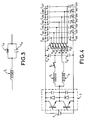
- FIG. 1 provides a better understanding of the general principle of the invention.
- a DC voltage source 1 is for example made by rectifying a 230 V AC voltage.
- the embodiment of the DC voltage source 1 is not shown in FIG. 1.
- the structure of an inverter 2 is in half bridge.
- This inverter 2 comprises two transistors T A and T B connected in series between the two positive and negative terminals of the DC voltage source 1.
- IGBT Insulated Gate Bipolar Transistor
- the means for controlling the two transistors T A and T B by their base is not shown in FIG. 1.
- This means essentially controls the frequency f T at which the transistors T A and T B are conductive and lock.
- An exemplary embodiment of such a control means is described in patent GB 2 175 154.
- the inverter 2 advantageously comprises two diodes D A and D B called freewheeling diodes.
- the cathode of the diode D A is connected to the positive pole of the DC voltage source 1.
- the anode of the diode D A and the cathode of the diode D B are connected to the junction point J of the two transistors T A and T B.
- the anode of D B is connected to the negative pole of the DC voltage source 1.
- the inverter 2 advantageously comprises two capacitors C A and C B for switching the transistors T A and T B.
- C A is connected between the positive pole of the DC voltage source 1 and the junction point J.
- C B is connected between the junction point J and the negative pole of the DC voltage source 1.
- the inverter 2 transmits the energy of the DC voltage source 1 to several resonant circuits connected in parallel. These resonant circuits are represented inside the frame 3 of FIG. 1. These resonant circuits are connected between the junction point J and the positive and negative poles of the DC voltage source 1.
- FIG. 1 represents only two circuits resonant, it is understood that the invention is not limited to the supply of two resonant circuits and it can be implemented for a greater number of resonant circuits.
- Each resonant circuit comprises an inductor referenced I 1 for the first resonant circuit and I 2 for the second resonant circuit.
- the first resonant circuit further comprises a switch K 1 and two capacitors C 11 and C 12 .
- the second resonant circuit further comprises a switch K 2 and two capacitors C 21 and C 22 .
- the switches K 1 and K 2 are for example relays.
- the inductors I 1 and I 2 are both connected by one of their terminal at the junction point J.
- the other terminal of the inductor I 1 is connected to a first terminal of the switch K 1 .
- the second terminal of the switch K 1 is connected to a first terminal of the two capacitors C 11 and C 12 .
- the second terminal of the capacitor C 11 is connected to the positive pole of the DC voltage source 1.
- the second terminal of the capacitor C 12 is connected to the negative pole of the DC voltage source 1.
- the other terminal of the inductor I 2 is connected to a first terminal of the switch K 2 .
- the second terminal of the switch K 2 is connected to a first terminal of the two capacitors C 21 and C 22 .
- the second terminal of the capacitor C 21 is connected to the positive pole of the DC voltage source 1.
- the second terminal of the capacitor C 22 is connected to the negative pole of the DC voltage source 1.
- Each resonant circuit can be likened to an RLC circuit.
- the inductor I 1 can be likened to an inductance L 1 connected in series with a resistance not shown. It is noted that the inductance L 1 may vary depending on the kitchen utensil placed on the inductor.
- the two capacitors C 11 and C 12 can be considered in parallel and thus equated with a single capacitor C 1 equal to C 11 + C 12 .
- the capacitances C 11 and C 12 will advantageously be chosen so that their nominal value is equal.
- the first resonant circuit can therefore be likened to a resistor R 1 , an inductance L 1 and a capacitor C 1 , all three connected in series.
- the same reasoning can be done for the second resonant circuit of which L 2 is the inductance of the inductor I 2 and C 2 is a value equal to the sum of the capacitances C 21 and C 22 .
- each switch K1 or K2 The role of each switch K1 or K2 is to turn on or off the inductor I1 or I2 with which it is connected.
- the two switches K 1 and K 2 When the two switches K 1 and K 2 are open, no inductor is powered.
- the operation of the device returns to the operation of the prior art mentioned above where associates for each inductor, a separate power generator.
- the device according to the invention is of interest when the two switches are closed. However, for an induction hob, it is necessary to provide the opening of the switches to allow the user the choice to use or not multiple inductors simultaneously. Consequently, for the rest of the presentation, it is assumed that the two switches K 1 and K 2 are closed.
- L 1 60 ⁇ H
- R1 20.5 kHz.
- the capacitance C 1 is given by two capacitors C 11 and C 12 each of 500 nF.
- the inductor I 1 When the working frequency f T of the inverter is equal to the resonant frequency f R1 , the inductor I 1 generates in the kitchen utensil as much power as possible and when the inverter is controlled so as to distance the working frequency f T of the resonance frequency f R1 , the power generated by the inductor I 1 decreases.
- L 2 60 ⁇ H
- C 2 0.5 ⁇ F.
- R2 29 kHz.
- Different values for C 1 and C 2 were chosen voluntarily so that the resonance frequencies f R1 and f R2 are distinct.
- the working frequency f T is varied, it is possible to obtain a power variation generated by each inductor.
- the working frequency f T is equal to the resonant frequency f R1 of the first resonant circuit, then the power generated by the first inductor I 1 which is large and the power generated by the second inductor I 2 which is low.
- the working frequency f T is increased , then the power generated by the first inductor I 1 decreases and as long as the working frequency f T is lower than the resonance frequency f R2 of the second resonant circuit , the power generated by the second inductor I 2 increases. It is possible to increase the working frequency f T beyond the resonance frequency f R2 ; then the power generated by the inductor I 2 decreases, after having gone through a maximum when the working frequency f T was equal to the resonance frequency f R2 .
- the working frequency f T is less than the smallest of the resonant frequencies, f R1 in the example chosen.
- the operating frequency f T is not varied from a value lower than f R1 to a value greater than f R2 . It is indeed preferable to vary the working frequency f T so that the output current of the inverter, that is to say between the J junction point and the resonant circuits, is always late on the voltage at point J, or is always ahead. This choice makes it possible to simplify the control strategy of the transistors T A and T B.
- FIG. 2 represents the general block diagram of the invention adapted to a complete bridge structure of the inverter.
- the inverter comprises four transistors T A , T B , T C , T D shown in two dashed frames 21 and 22.
- T A and T B are in the frame 21;
- T C and T D are in the frame 22.
- the transistors T A and T B on the one hand, T C and T D on the other hand are connected in series between the two poles of the DC voltage source 1.
- the point junction of the two transistors T A and T B is marked J 21 .
- the junction point of the two transistors T C and T D is marked J 22 .
- the frames 21 and 22 there is no representation of freewheeling diodes nor switching capacitors, but it is understood that these components may exist.
- the inverter 21, 22 transmits energy to two resonant circuits.
- FIG. 2 represents only two resonant circuits and their selection means K 1 and K 2 .
- the first resonant circuit comprises in series the following elements: an inductor I 1 , a capacitor C 1 and a switch K 1 .
- the second resonant circuit comprises in series an inductor I 2 , a capacitor C 2 and a switch K 2 .
- the value of the capacitor C 1 of FIG. 2 is equal to the sum of the values of the capacitors C 11 and C 12 described in FIG. 1. If C 11 and C 12 each have a value of 500 nF, then C 1 has a value of 1 ⁇ F.
- the operation of the device described in FIG. 2 is similar to the operation of the device described in FIG. 1.
- the operating frequency of the inverter is varied to increase or decrease the powers generated by the inductors I 1 and I 2 .
- the full bridge structure has the advantage, for the same power generated by the inductors I 1 and I 2 , to reduce the intensity of the current flowing in each transistor.
- each resonant circuit is, for the same DC voltage source 1, subjected to a greater potential difference.
- inverter structures described in Figures 1 and 2 are given by way of example, other structures can be used in devices according to the invention.
- an inverter structure having only one transistor is known.
- This structure is known as a mono-switch structure, the use of a transistor being given only by way of example.
- the resonant circuits shown in FIGS. 1 and 2 are first-order resonant circuits. It is of course possible to use higher order circuits to implement the invention.
- An example of a second-order circuit is described in FIG. 3.
- This circuit is represented without the inverter which supplies it, it is of course conceivable to supply it with an inverter whatever its structure, for example a half-bridge or a complete bridge. or mono-switch.
- This circuit comprises, in series with the inductor I 1 , two components connected in parallel, a capacitor C 31 and an inductor L 31 .
- This circuit has two power maxima. This makes it possible to adjust, with greater flexibility, the relative powers consumed by the inductors of several resonant circuits connected in parallel.
- the different resonant circuits are not necessarily all of the same order.
- FIG. 4 gives an example of means making it possible to vary the resonance frequency f R2 of the second resonant circuit and thus to improve the flexibility of adjustment of the powers generated by the two inductors I 1 and I 2 .
- the first resonant circuit is identical to that shown in FIG. 1.
- the second resonant circuit also comprises, as in FIG. 1, the inductor I 2 , but unlike FIG. 1, the second resonant circuit comprises several switches K 21. at K 27 connected by their first terminal to the inductor terminal I 2 not connected to the inverter 2.
- the second terminal of the switch K 21 is connected to a first terminal of two capacitors C 211 and C 212 .
- the second terminal of the capacitor C 211 is connected to the positive pole of the DC voltage source 1 and the second terminal of the capacitor C 212 is connected to the negative pole of the DC voltage source 1.
- the second terminal of each other switch K 22 to K 27 is connected to a first terminal of two capacitors whose second terminal is connected either to the positive pole or to the negative pole of the DC voltage source.
- the switch K 2i corresponds the capacitance C 2i1 connected to the positive pole and the capacitance C 2i2 connected to the negative pole.
- i varies from 1 to 7. It is understood that the invention is not limited to 7 structures each comprising a switch and two capacitors.
- FIG. 4 gives an example of a device making it possible to vary the capacitance of the second resonant circuit.
- the variation of the capacitance makes it possible to vary the resonance frequency f R2 and thus to adjust the power generated by each of the two inductors I 1 and I 2 independently of one another.
- the switch K 1 When the switch K 1 is closed, the working frequency f T of the inverter is set according to the power that it is desired to generate by the inductor I 1 . Then, to adjust the power that it is desired to generate by inductor I 2 , one or more switches K 2i are closed so as to vary the resonant frequency f R2 of the second resonant circuit.
- the K 2i switches have the function of switching on or off the inductors. In addition, they are manipulated when the user wants to change the power of one of the inductors. In steady state, ie in the absence of modification setpoint by the user of the power to be generated, the switches are not maneuvered and the inductors are therefore permanently powered by the inverter 2, when in use.
- the embodiment described in FIG. 4 makes it possible to vary the resonant frequency in successive steps.
- the capacities for varying the resonance frequency are associated in parallel, it is possible to associate them in series with switches to short-circuit them. We can also combine the serial and parallel association. If on the other hand we wish to vary this frequency smoothly, it is possible to replace the switches and the capacity of the second resonant circuit by a single switch, allowing the resonant circuit break and one or more variable capacitances.
- each additional resonant circuit will also comprise, as the second resonant circuit, means for varying its resonance frequency.
- master circuit first resonant circuit of Figure 4
- slave circuits Other circuits whose resonance frequency can be set.
- the resonance frequency of the slave circuits is set so that it is equal to the resonance frequency of the master circuit.
- the working frequency f T is adjusted in the vicinity of the resonance frequency of the resonant circuits.
- the inverter can deliver the sum of the nominal powers of each resonant circuit.
- the inverter thus dimensioned has the advantage of being able to supply one or more particular resonant circuits at a power greater than its nominal power when the other circuits are powered at a power lower than their nominal power. Thus, it distributes at will the maximum power available at the output of the inverter to different inductors.
- the power generator it is even possible to allow the power generator to deliver all its available power to an inductor for a limited period of time, for example a few minutes, which is, of course, less than the thermal time constant of the inductor.
- the order of magnitude of the thermal time constant of an inductor can be 30 minutes, which is very significantly greater than the time required for certain cooking preparations.
- a pasta cooking mode We start by boiling water with high power and after having immersed the pasta in boiling water, we reduce the power to keep the simmering water. In order to reduce the time of the first phase, which consists in bringing water to a boil, it is interesting to increase as much as possible the power generated by the inductor.
Description
L'invention se rapporte à un dispositif d'alimentation de plusieurs inducteurs par un générateur de puissance à onduleur.The invention relates to a device for supplying a plurality of inductors by an inverter power generator.
Il est connu d'utiliser un générateur de puissance à onduleur pour alimenter un inducteur monté en série avec un condensateur. L'inducteur peut être assimilé à une inductance et une résistance. L'inducteur et le condensateur forment alors un circuit résonant connu sous le nom de circuit RLC. Le générateur de puissance, alimentant ce circuit résonant, comporte par exemple un redresseur d'une tension secteur alternative suivi d'un onduleur comprenant deux transistors. Pour régler la puissance absorbée par le circuit résonant, on peut agir sur la fréquence de cycles successifs de conduction et de non conduction des transistors. Par la suite, on appellera cette fréquence, fréquence de travail fT. On peut aussi agir sur le rapport entre les durées de conduction et de non conduction des transistors, sur une période de travail.It is known to use an inverter power generator for supplying an inductor connected in series with a capacitor. The inductor can be likened to inductance and resistance. The inductor and the capacitor then form a resonant circuit known as the RLC circuit. The power generator supplying this resonant circuit comprises, for example, a rectifier of an AC mains voltage followed by an inverter comprising two transistors. To adjust the power absorbed by the resonant circuit, it is possible to influence the frequency of successive cycles of conduction and non-conduction of the transistors. Subsequently, this frequency will be called the working frequency f T. One can also act on the ratio between the conduction and non-conduction times of the transistors, over a period of work.
Dans une table de cuisson à induction, on a le plus souvent plusieurs inducteurs. Il est connu d'utiliser pour chaque inducteur un générateur de puissance distinct. Un premier inconvénient de cette solution concerne le prix. En effet, un générateur est un élément onéreux. Un autre inconvénient de cette solution est qu'elle peut entraîner des interférences entre les différents sous-ensembles. On définit ici un sous-ensemble comme comportant un générateur et le circuit résonant qu'il alimente. En effet, lorsque deux sous-ensembles fonctionnent à des fréquences de travail voisines, certains composants, électriques ou mécaniques peuvent être excités à une fréquence égale à la différence entre les fréquences de travail des deux sous-ensembles. Cela peut, entre autres inconvénients, conduire à des bruits audibles gênants pour un utilisateur.In an induction hob, we often have several inductors. It is known to use for each inductor a separate power generator. A first disadvantage of this solution is the price. Indeed, a generator is an expensive element. Another disadvantage of this solution is that it can cause interference between the different subsets. A subset is defined here as comprising a generator and the resonant circuit that it supplies. Indeed, when two subsets operate at neighboring working frequencies, some electrical or mechanical components can be excited at a frequency equal to the difference between the working frequencies of the two subsets. This can, among other disadvantages, lead to annoying audible noises for a user.
Pour pallier ces inconvénients, d'autres dispositifs ont été conçus pour n'utiliser qu'un seul générateur servant à alimenter plusieurs inducteurs. Ces dispositifs prévoient d'alimenter chaque inducteur de façon cyclique, c'est-à-dire l'un après l'autre. Ces dispositifs nécessitent des moyens de commutation rapide. Ces moyens, relais ou semi-conducteurs, sont généralement onéreux. Ils peuvent être bruyants dans le cas de relais.To overcome these disadvantages, other devices have been designed to use a single generator for supplying multiple inductors. These devices provide for feeding each inductor cyclically, that is to say one after the other. These devices require fast switching means. These means, relays or semiconductors, are generally expensive. They can be noisy in the case of relays.
Ils peuvent entraîner des perturbations sur la tension secteur en y puisant la puissance de façon saccadée. US-A-4092510 divulgue un dispositif d'alimentation de plusieurs inducteurs par un générateur à onduleur dans lequel la puissance consommée par chaque circuit résonant est réglée en modifiant l'impédance de chaque circuit résonant.They can cause disturbances to the mains voltage by drawing the power jerkily. US-A-4092510 discloses a device for supplying several inductors by an inverter generator in which the power consumed by each resonant circuit is adjusted by modifying the impedance of each resonant circuit.
L'invention à pour but de pallier les inconvénients précédemment cités en n'utilisant qu'un seul générateur pour alimenter plusieurs inducteurs sans utiliser de moyens de commutation rapide. La cuisson domestique par induction est un domaine où l'invention trouve une utilité particulière. Mais il est bien entendu que l'invention n'est pas limitée à ce domaine, elle peut être mise en oeuvre chaque fois qu'on souhaite alimenter plusieurs circuits résonants, quelque soit le domaine d'utilisation : cuisson domestique ou autre.The invention aims to overcome the disadvantages mentioned above by using a single generator to power multiple inductors without using fast switching means. Induction cooking is a field where the invention finds particular utility. But it is understood that the invention is not limited to this field, it can be implemented whenever it is desired to supply several resonant circuits, whatever the field of use: domestic cooking or other.
Pour atteindre ce but, l'invention a pour objet un dispositif d'alimentation de plusieurs circuits résonants montés en parallèle par un générateur de puissance à onduleur. Le dispositif est caractérisé en ce que chaque circuit résonant a une fréquence de résonance distincte, en ce que le générateur alimente en permanence les circuits résonants et en ce que le réglage de la puissance consommée par chaque circuit résonant est réalisé en modifiant la fréquence de travail de l'onduleur.To achieve this object, the invention relates to a device for supplying a plurality of resonant circuits connected in parallel by an inverter power generator. The device is characterized in that each resonant circuit has a distinct resonant frequency, in that the generator continuously supplies the resonant circuits and in that the adjustment of the power consumed by each resonant circuit is achieved by modifying the working frequency of the inverter.
L'invention sera mieux comprise et d'autres avantages apparaîtront à la lecture de la description détaillée d'un mode de réalisation illustré par le dessin annexé, sur lequel :
- la figure 1 représente le schéma de principe général de l'invention adapté à une structure demi-pont de l'onduleur;
- la figure 2 représente le schéma de principe général de l'invention adapté à une structure en pont complet de l'onduleur :
- la figure 3 représente le schéma d'une variante d'un circuit résonant du troisième ordre ;
- la figure 4 représente le schéma de principe général de l'invention où plusieurs capacités peuvent être mises en parallèles.
- Figure 1 shows the general block diagram of the invention adapted to a half-bridge structure of the inverter;
- FIG. 2 represents the general block diagram of the invention adapted to a complete bridge structure of the inverter:
- FIG. 3 represents the diagram of a variant of a resonant circuit of the third order;
- Figure 4 shows the general block diagram of the invention where several capabilities can be paralleled.
Par souci de simplicité, les mêmes éléments porteront les mêmes références dans les différentes figures.For the sake of simplicity, the same elements will bear the same references in the different figures.
La figure 1 permet de mieux comprendre le principe général de l'invention. Une source de tension continue 1 est par exemple réalisée en redressant une tension secteur alternative 230 V. Le mode de réalisation de la source de tension continue 1 n'est pas représenté en figure 1. La structure d'un onduleur 2 est en demi-pont. Cet onduleur 2 comporte deux transistors TA et TB montés en série entre les deux bornes positive et négative de la source de tension continue 1. On a choisi de représenter deux transistors bipolaires TA et TB, mais il est bien entendu que l'onduleur 2 peut fonctionner avec tous moyens de commutation électronique comme par exemple des thyristors, des transistors à effet de champ ou des interrupteurs de type transistor commandés en tension, connus dans la littérature anglosaxonne sous le nom de IGBT (Insulated Gate Bipolar Transistor). Le moyen de commande des deux transistors TA et TB par leur base n'est pas représenté sur la figure 1. Ce moyen commande essentiellement la fréquence fT à laquelle les transistors TA et TB sont conducteurs et se bloquent. Un exemple de réalisation d'un tel moyen de commande est décrit dans le brevet GB 2 175 154. De plus, l'onduleur 2 comporte avantageusement deux diodes DA et DB appelées diodes de roue libre. La cathode de la diode DA est raccordée au pôle positif de la source de tension continue 1. L'anode de la diode DA et la cathode de la diode DB sont raccordées au point de jonction J des deux transistors TA et TB. L'anode de DB est raccordée au pôle négatif de la source de tension continue 1. En outre, l'onduleur 2 comporte avantageusement deux capacités CA et CB d'aide à la commutation des transistors TA et TB. CA est raccordé entre le pôle positif de la source de tension continue 1 et le point de jonction J. CB est raccordé entre le point de jonction J et le pôle négatif de la source de tension continue 1.Figure 1 provides a better understanding of the general principle of the invention. A DC voltage source 1 is for example made by rectifying a 230 V AC voltage. The embodiment of the DC voltage source 1 is not shown in FIG. 1. The structure of an inverter 2 is in half bridge. This inverter 2 comprises two transistors T A and T B connected in series between the two positive and negative terminals of the DC voltage source 1. We have chosen to represent two bipolar transistors T A and T B , but it is understood that the inverter 2 can operate with any electronic switching means such as thyristors, field effect transistors or voltage-controlled transistor type switches, known in the English literature as the IGBT (Insulated Gate Bipolar Transistor). The means for controlling the two transistors T A and T B by their base is not shown in FIG. 1. This means essentially controls the frequency f T at which the transistors T A and T B are conductive and lock. An exemplary embodiment of such a control means is described in patent GB 2 175 154. In addition, the inverter 2 advantageously comprises two diodes D A and D B called freewheeling diodes. The cathode of the diode D A is connected to the positive pole of the DC voltage source 1. The anode of the diode D A and the cathode of the diode D B are connected to the junction point J of the two transistors T A and T B. The anode of D B is connected to the negative pole of the DC voltage source 1. In addition, the inverter 2 advantageously comprises two capacitors C A and C B for switching the transistors T A and T B. C A is connected between the positive pole of the DC voltage source 1 and the junction point J. C B is connected between the junction point J and the negative pole of the DC voltage source 1.
L'onduleur 2 transmet l'énergie de la source de tension continue 1 à plusieurs circuits résonants montés en parallèle. Ces circuits résonants sont représentés à l'intérieur du cadre 3 de la figure 1. Ces circuits résonants sont raccordés entre le point de jonction J et les pôles positif et négatif de la source de tension continue 1. La figure 1 ne représente que deux circuits résonants, il est bien entendu que l'invention ne se limite pas à l'alimentation de deux circuits résonants et qu'elle peut être mise en oeuvre pour un plus grand nombre de circuits résonants.The inverter 2 transmits the energy of the DC voltage source 1 to several resonant circuits connected in parallel. These resonant circuits are represented inside the
Chaque circuit résonant comporte un inducteur référencé I1 pour le premier circuit résonant et I2 pour le deuxième circuit résonant. Le premier circuit résonant comporte en outre un interrupteur K1 et deux capacités C11 et C12. Le deuxième circuit résonant comporte en outre un interrupteur K2 et deux capacités C21 et C22. Les interrupteurs K1 et K2 sont par exemple des relais. Les inducteurs I1 et I2 sont raccordées tous deux par une de leur borne au point de jonction J. L'autre borne de l'inducteur I1 est raccordée à une première borne de l'interrupteur K1. La deuxième borne de l'interrupteur K1 est raccordée à une première borne des deux capacités C11 et C12. La deuxième borne de la capacité C11 est raccordée au pôle positif de la source de tension continue 1. La deuxième borne de la capacité C12 est raccordée au pôle négatif de la source de tension continue 1. L'autre borne de l'inducteur I2 est raccordée à une première borne de l'interrupteur K2. La deuxième borne de l'interrupteur K2 est raccordée a une première borne des deux capacités C21 et C22. La deuxième borne de la capacité C21 est raccordée au pôle positif de la source de tension continue 1. La deuxième borne de la capacité C22 est raccordée au pôle négatif de la source de tension continue 1.Each resonant circuit comprises an inductor referenced I 1 for the first resonant circuit and I 2 for the second resonant circuit. The first resonant circuit further comprises a switch K 1 and two capacitors C 11 and C 12 . The second resonant circuit further comprises a switch K 2 and two capacitors C 21 and C 22 . The switches K 1 and K 2 are for example relays. The inductors I 1 and I 2 are both connected by one of their terminal at the junction point J. The other terminal of the inductor I 1 is connected to a first terminal of the switch K 1 . The second terminal of the switch K 1 is connected to a first terminal of the two capacitors C 11 and C 12 . The second terminal of the capacitor C 11 is connected to the positive pole of the DC voltage source 1. The second terminal of the capacitor C 12 is connected to the negative pole of the DC voltage source 1. The other terminal of the inductor I 2 is connected to a first terminal of the switch K 2 . The second terminal of the switch K 2 is connected to a first terminal of the two capacitors C 21 and C 22 . The second terminal of the capacitor C 21 is connected to the positive pole of the DC voltage source 1. The second terminal of the capacitor C 22 is connected to the negative pole of the DC voltage source 1.
Chaque circuit résonant peut être assimilé à un circuit RLC. En effet, pour le premier circuit résonant, l'inducteur I1 peut être assimilé à une inductance L1 montée en série avec une résistance non représentée. On note que l'inductance L1 peut varier en fonction de l'ustensile de cuisine posé sur l'inducteur. En régime alternatif, les deux capacités C11 et C12 peuvent être considérées en parallèle et donc assimilées à une seule capacité C1 égale à C11 + C12. En pratique, on choisira avantageusement les capacités C11 et C12 de telle sorte que leur valeur nominale soit égale. Le premier circuit résonant peut donc être assimilé à une résistance R1, une inductance L1 et une capacité C1, toutes trois montées en série. La fréquence de résonance fR1 de ce premier circuit résonant peut être calculée suivant la formule ![]()
![]()
Le même raisonnement peut être fait pour le deuxième circuit résonant dont L2 est l'inductance de l'inducteur I2 et C2 est une valeur égale à la somme des capacités C21 et C22. La fréquence de résonance fR2 du deuxième circuit résonant peut alors être calculée suivant la formule ![]()
![]()
Le rôle de chaque interrupteur K1 ou K2 est de mettre en/ou hors service l'inducteur I1 ou I2 avec lequel il est raccordé. Lorsque les deux interrupteurs K1 et K2 sont ouverts, aucun inducteur n'est alimenté. Lorsqu'un seul des interrupteurs K1 ou K2 est fermé, le fonctionnement du dispositif revient au fonctionnement de l'art antérieur cité plus haut où on associe pour chaque inducteur, un générateur de puissance distinct. Le dispositif conforme à l'invention présente de l'intérêt quand les deux interrupteurs sont fermés. Néanmoins, pour une table de cuisson à induction, il est nécessaire de prévoir l'ouverture des interrupteurs pour laisser à l'utilisateur le choix d'utiliser ou non plusieurs inducteurs simultanément. En conséquence, pour la suite de l'exposé, on suppose que les deux interrupteurs K1 et K2 sont fermés.The role of each switch K1 or K2 is to turn on or off the inductor I1 or I2 with which it is connected. When the two switches K 1 and K 2 are open, no inductor is powered. When only one of the switches K 1 or K 2 is closed, the operation of the device returns to the operation of the prior art mentioned above where associates for each inductor, a separate power generator. The device according to the invention is of interest when the two switches are closed. However, for an induction hob, it is necessary to provide the opening of the switches to allow the user the choice to use or not multiple inductors simultaneously. Consequently, for the rest of the presentation, it is assumed that the two switches K 1 and K 2 are closed.
A titre d'exemple, pour mieux comprendre l'invention, on donne les valeurs suivantes pour le premier circuit résonant : L1 = 60 µH, C1 = 1 µF. On a donc fR1 = 20,5 kHz. La valeur L1 = 60 µH est donnée pour un ustensile de cuisine donné, posé sur l'inducteur. Il est bien entendu que cette valeur varie en fonction des dimensions et du matériau de l'ustensile de cuisine. Bien entendu, la capacité C1 est donnée par deux capacités C11 et C12 chacune de valeur 500 nF. Lorsque la fréquence de travail fT de l'onduleur est égale à la fréquence de résonance fR1, l'inducteur I1 génère dans l'ustensile de cuisine la plus grande puissance possible et lorsqu'on commande l'onduleur de façon à éloigner la fréquence de travail fT de la fréquence de résonance fR1, la puissance générée par l'inducteur I1 diminue. Pour les composants du deuxième circuit résonant, on donne les valeurs suivantes : L2 = 60 µH, C2 = 0,5 µF. On a donc fR2 = 29 kHz. On a choisi volontairement des valeurs différentes pour C1 et C2 pour que les fréquences de résonance fR1 et fR2 soient distinctes. Ainsi, lorsqu'on fait varier la fréquence de travail fT, on peut obtenir une variation de puissance générée par chaque inducteur. Par exemple si la fréquence de travail fT est égale à la fréquence de résonance fR1 du premier circuit résonant, on a alors la puissance générée par le premier inducteur I1 qui est grande et la puissance générée par le deuxième inducteur I2 qui est faible.By way of example, to better understand the invention, the following values are given for the first resonant circuit: L 1 = 60 μH, C 1 = 1 μF. We therefore have R1 = 20.5 kHz. The value L 1 = 60 μH is given for a given kitchen utensil placed on the inductor. It is understood that this value varies according to the dimensions and the material of the kitchen utensil. Of course, the capacitance C 1 is given by two capacitors C 11 and C 12 each of 500 nF. When the working frequency f T of the inverter is equal to the resonant frequency f R1 , the inductor I 1 generates in the kitchen utensil as much power as possible and when the inverter is controlled so as to distance the working frequency f T of the resonance frequency f R1 , the power generated by the inductor I 1 decreases. For the components of the second resonant circuit, the following values are given: L 2 = 60 μH, C 2 = 0.5 μF. Thus R2 = 29 kHz. Different values for C 1 and C 2 were chosen voluntarily so that the resonance frequencies f R1 and f R2 are distinct. Thus, when the working frequency f T is varied, it is possible to obtain a power variation generated by each inductor. For example, if the working frequency f T is equal to the resonant frequency f R1 of the first resonant circuit, then the power generated by the first inductor I 1 which is large and the power generated by the second inductor I 2 which is low.
Si par la suite, on augmente la fréquence de travail fT, on a alors la puissance générée par le premier inducteur I1 qui diminue et tant que la fréquence de travail fT est inférieure à la fréquence de résonance fR2 du deuxième circuit résonant, la puissance générée par le deuxième inducteur I2 augmente. On peut augmenter la fréquence de travail fT au delà de la fréquence de résonance fR2 ; alors la puissance générée par l'inducteur I2 décroît, après être passée par un maximum lorsque la fréquence de travail fT était égale à la fréquence de résonance fR2. On peut bien entendu imaginer que la fréquence de travail fT soit inférieure à la plus petite des fréquences de résonance, fR1 dans l'exemple choisi. Ainsi, lorsque les deux interrupteurs K1 et K2 sont fermés, en faisant varier la fréquence de travail fT, on peut faire croître et décroître les puissances générée par les deux inducteurs. En régime établi, c'est à dire en l'absence de modification consigne de la part de l'utilisateur, les interrupteurs ne sont pas manoeuvrés et les inducteurs, sont donc alimentés en permanence par l'onduleur 2, lorsqu'ils sont en serviceIf, subsequently, the working frequency f T is increased , then the power generated by the first inductor I 1 decreases and as long as the working frequency f T is lower than the resonance frequency f R2 of the second resonant circuit , the power generated by the second inductor I 2 increases. It is possible to increase the working frequency f T beyond the resonance frequency f R2 ; then the power generated by the inductor I 2 decreases, after having gone through a maximum when the working frequency f T was equal to the resonance frequency f R2 . We can of course imagine that the working frequency f T is less than the smallest of the resonant frequencies, f R1 in the example chosen. Thus, when the two switches K 1 and K 2 are closed, by varying the working frequency f T , it is possible to increase and decrease the powers generated by the two inductors. In steady state, that is to say in the absence of modification set by the user, the switches are not operated and the inductors, are therefore permanently powered by the inverter 2, when they are in service
Avantageusement, pour simplifier les moyens de commande des deux transistors TA et TB, on ne fait pas varier la fréquence de travail fT depuis une valeur inférieure à fR1 jusqu'à une valeur supérieure à fR2. Il est en effet préférable de faire varier la fréquence de travail fT de telle sorte que le courant en sortie de l'onduleur, c'est-à-dire entre le point de jonction J et les circuits résonants, soit toujours en retard sur la tension au point J, ou soit toujours en avance. Ce choix permet de simplifier la stratégie de commande des transistors TA et TB.Advantageously, to simplify the control means of the two transistors T A and T B , the operating frequency f T is not varied from a value lower than f R1 to a value greater than f R2 . It is indeed preferable to vary the working frequency f T so that the output current of the inverter, that is to say between the J junction point and the resonant circuits, is always late on the voltage at point J, or is always ahead. This choice makes it possible to simplify the control strategy of the transistors T A and T B.
La figure 2 représente le schéma de principe général de l'invention adapté à une structure en pont complet de l'onduleur. L'onduleur comporte quatre transistors TA, TB, TC, TD représentés dans deux cadres en traits interrompus 21 et 22. TA et TB sont dans le cadre 21 ; TC et TD sont dans le cadre 22. Les transistors TA et TB d'une part, TC et TD d'autre part sont montés en série entre les deux pôles de la source de tension continue 1. Le point de jonction des deux transistors TA et TB porte le repère J21. Le point de jonction des deux transistors TC et TD porte le repère J22. Par souci de simplicité, dans les cadres 21 et 22 on n'a pas représenté de diodes de roue libre ni de condensateurs d'aide à la commutation, mais il est bien entendu que ces composants peuvent exister.FIG. 2 represents the general block diagram of the invention adapted to a complete bridge structure of the inverter. The inverter comprises four transistors T A , T B , T C , T D shown in two dashed
L'onduleur 21, 22, transmet de l'énergie à deux circuits résonants. La figure 2 ne représente que deux circuits résonants et leurs moyens de sélection K1 et K2. Comme pour la figure 1 il est bien entendu que l'invention peut être mise en oeuvre pour un plus grand nombre de circuits résonants. Ces deux circuits résonants sont montés en parallèle entre les points de jonction J21 et J22. Le premier circuit résonant comporte en série les éléments suivants : un inducteur I1, une capacité C1 et un interrupteur K1. Le deuxième circuit résonant comporte en série un inducteur I2, une capacité C2 et un interrupteur K2. Pour que le premier circuit résonant, décrit en figure 1, soit équivalent au premier circuit résonant décrit en figure 2, il suffit que la valeur de la capacité C1 de la figure 2 soit égale à la somme des valeurs des capacités C11 et C12 décrites en figure 1. Si C11 et C12 ont chacune pour valeur 500 nF, alors C1 a pour valeur 1 µF. Le fonctionnement du dispositif décrit à la figure 2 est semblable au fonctionnement du dispositif décrit à la figure 1. On fait varier la fréquence de travail de l'onduleur pour faire croître ou décroître les puissances générées par les inducteurs I1 et I2.The
La structure en pont complet présente l'avantage, pour une même puissance générée par les inducteurs I1 et I2, de réduire l'intensité du courant passant dans chaque transistor. En revanche chaque circuit résonant est, pour une même source de tension continue 1, soumis à une plus forte différence de potentiel.The full bridge structure has the advantage, for the same power generated by the inductors I 1 and I 2 , to reduce the intensity of the current flowing in each transistor. On the other hand each resonant circuit is, for the same DC voltage source 1, subjected to a greater potential difference.
Les deux structures d'onduleur décrites en figures 1 et 2 ne sont données qu'à titre d'exemple, d'autres structures sont utilisables dans des dispositifs conformes à l'invention. On connaît par exemple une structure d'onduleur ne comportant qu'un seul transistor. Cette structure est connue sous le nom de structure mono-interrupteur, l'utilisation d'un transistor n'étant en effet donnée qu'à titre d'exemple.The two inverter structures described in Figures 1 and 2 are given by way of example, other structures can be used in devices according to the invention. For example, an inverter structure having only one transistor is known. This structure is known as a mono-switch structure, the use of a transistor being given only by way of example.
Les circuits résonants représentés en figures 1 et 2 sont des circuits résonants du premier ordre. Il est bien entendu possible d'utiliser des circuits d'ordre supérieur pour mettre en oeuvre l'invention. Un exemple de circuit du deuxième ordre est décrit figure 3. Ce circuit est représenté sans l'onduleur qui l'alimente, il est bien sûr envisageable de l'alimenter avec un onduleur quelque soit sa structure comme par exemple demi-pont, pont complet ou mono-interrupteur. Ce circuit comporte, en série avec l'inducteur I1, deux composants montés en parallèle, une capacité C31 et une inductance L31. Ce circuit présente deux maxima de puissance. Ceci permet de pouvoir régler, avec plus de souplesse, les puissances relatives consommées par les inducteurs de plusieurs circuits résonants raccordés en parallèle. Les différents circuits résonants ne sont pas obligatoirement tous du même ordre.The resonant circuits shown in FIGS. 1 and 2 are first-order resonant circuits. It is of course possible to use higher order circuits to implement the invention. An example of a second-order circuit is described in FIG. 3. This circuit is represented without the inverter which supplies it, it is of course conceivable to supply it with an inverter whatever its structure, for example a half-bridge or a complete bridge. or mono-switch. This circuit comprises, in series with the inductor I 1 , two components connected in parallel, a capacitor C 31 and an inductor L 31 . This circuit has two power maxima. This makes it possible to adjust, with greater flexibility, the relative powers consumed by the inductors of several resonant circuits connected in parallel. The different resonant circuits are not necessarily all of the same order.
La figure 4 donne un exemple de moyen permettant de faire varier la fréquence de résonance fR2 du deuxième circuit résonant et ainsi d'améliorer la souplesse de réglage des puissances générées par les deux inducteurs I1 et I2. Le premier circuit résonant est identique à celui représenté à la figure 1. Le second circuit résonant comporte aussi, comme à la figure 1 l'inducteur I2, mais à la différence de la figure 1, le deuxième circuit résonant comporte plusieurs interrupteurs K21 à K27 raccordés par leur première borne à la borne de l'inducteur I2 non raccordée à l'onduleur 2. La deuxième borne de l'interrupteur K21 est reliée à une première borne de deux capacités C211 et C212. La deuxième borne de la capacité C211 est reliée au pôle positif de la source de tension continue 1 et la deuxième borne de la capacité C212 est reliée au pôle négatif de la source de tension continue 1. Comme pour l'interrupteur K21, la deuxième borne de chaque autre interrupteur K22 à K27 est raccordée à une première borne de deux capacités dont la deuxième borne est raccordée soit au pôle positif soit au pôle négatif de la source de tension continue. A l'interrupteur K2i correspond la capacité C2i1 reliée au pôle positif et la capacité C2i2 reliée au pôle négatif. Dans la représentation de la figure 4, i varie de 1 à 7. Il est bien entendu que l'invention n'est pas limitée à 7 structures comprenant chacune un interrupteur et deux capacités.FIG. 4 gives an example of means making it possible to vary the resonance frequency f R2 of the second resonant circuit and thus to improve the flexibility of adjustment of the powers generated by the two inductors I 1 and I 2 . The first resonant circuit is identical to that shown in FIG. 1. The second resonant circuit also comprises, as in FIG. 1, the inductor I 2 , but unlike FIG. 1, the second resonant circuit comprises several switches K 21. at K 27 connected by their first terminal to the inductor terminal I 2 not connected to the inverter 2. The second terminal of the switch K 21 is connected to a first terminal of two capacitors C 211 and C 212 . The second terminal of the capacitor C 211 is connected to the positive pole of the DC voltage source 1 and the second terminal of the capacitor C 212 is connected to the negative pole of the DC voltage source 1. As for the switch K 21 , the second terminal of each other switch K 22 to K 27 is connected to a first terminal of two capacitors whose second terminal is connected either to the positive pole or to the negative pole of the DC voltage source. At the switch K 2i corresponds the capacitance C 2i1 connected to the positive pole and the capacitance C 2i2 connected to the negative pole. In the representation of Figure 4, i varies from 1 to 7. It is understood that the invention is not limited to 7 structures each comprising a switch and two capacitors.
La figure 4 donne un exemple de dispositif permettant de faire varier la capacité du deuxième circuit résonant. La variation de la capacité permet de faire varier la fréquence de résonance fR2 et donc de régler la puissance générée par chacun des deux inducteurs I1 et I2 indépendamment l'un de l'autre. Lorsque l'interrupteur K1 est fermé, on règle la fréquence de travail fT de l'onduleur en fonction de la puissance que l'on souhaite générer par l'inducteur I1. Ensuite pour régler la puissance que l'on souhaite générer par l'inducteur I2, on ferme un ou plusieurs interrupteurs K2i de façon à faire varier la fréquence de résonance fR2 du deuxième circuit résonant. Lorsqu'on souhaite générer une puissance importante par l'inducteur I2, on ferme le ou les interrupteurs K2i nécessaires pour que la fréquence de résonance fR2 soit la plus proche possible de fT. Si au contraire, on souhaite générer une puissance plus faible par l'inducteur I2, on ferme le ou les interrupteurs K2i nécessaires pour que la fréquence de résonance fR2 s'éloigne de fT. Comme pour les variantes représentées figures 1 et 2, les interrupteurs K2i ont pour fonction la mise en ou hors service des inducteurs. De plus, ils sont manoeuvrés lorsque l'utilisateur souhaite modifier la puissance d'un des inducteurs. En régime permanent, c'est à dire en l'absence de modification de consigne par l'utilisateur de la puissance à générer, les interrupteurs ne sont pas manoeuvrés et les inducteurs sont donc alimentés en permanence par l'onduleur 2, lorsqu'il sont en service.FIG. 4 gives an example of a device making it possible to vary the capacitance of the second resonant circuit. The variation of the capacitance makes it possible to vary the resonance frequency f R2 and thus to adjust the power generated by each of the two inductors I 1 and I 2 independently of one another. When the switch K 1 is closed, the working frequency f T of the inverter is set according to the power that it is desired to generate by the inductor I 1 . Then, to adjust the power that it is desired to generate by inductor I 2 , one or more switches K 2i are closed so as to vary the resonant frequency f R2 of the second resonant circuit. When it is desired to generate a large power by the inductor I 2 , it is necessary to close the switch or switches K 2i so that the resonant frequency f R2 is as close as possible to f T. If, on the other hand, it is desired to generate a lower power by the inductor I 2 , the one or more switches K 2i are closed so that the resonance frequency f R2 moves away from f T. As for the variants shown in Figures 1 and 2, the K 2i switches have the function of switching on or off the inductors. In addition, they are manipulated when the user wants to change the power of one of the inductors. In steady state, ie in the absence of modification setpoint by the user of the power to be generated, the switches are not maneuvered and the inductors are therefore permanently powered by the inverter 2, when in use.
Le mode de réalisation décrit figure 4 permet de faire varier la fréquence de résonance par pas successifs. Les capacités permettant de faire varier la fréquence de résonance sont associées en parallèle, il est possible de les associer en série avec des interrupteurs permettant de les court-circuiter. On peut aussi combiner l'association série et parallèle. Si par contre on souhaite faire varier cette fréquence sans à coup, il est possible de remplacer les interrupteurs et les capacités du deuxième circuit résonant par un seul interrupteur, permettant la coupure du circuit résonant et une ou plusieurs capacités variables. De façon générale, on regroupera sous le nom de capacité modulable tout moyen permettant de faire varier la valeur d'une capacité que ce soit avec ou sans à coup.The embodiment described in FIG. 4 makes it possible to vary the resonant frequency in successive steps. The capacities for varying the resonance frequency are associated in parallel, it is possible to associate them in series with switches to short-circuit them. We can also combine the serial and parallel association. If on the other hand we wish to vary this frequency smoothly, it is possible to replace the switches and the capacity of the second resonant circuit by a single switch, allowing the resonant circuit break and one or more variable capacitances. In a general way, we will group under the name of flexible capacity any means allowing to vary the value of a capacity that it is with or without jerk.
On peut également imaginer, pour faire varier la fréquence de résonance du deuxième circuit résonant, de faire varier la valeur d'une inductance appartenant à ce circuit, comme par exemple l'inductance L1 ou L2 et/ou l'inductance L31 du circuit représenté figure 3. La variation de l'inductance peut se faire de façon continue ou pas à pas comme pour les condensateurs de la figure 4.One can also imagine, to vary the resonant frequency of the second resonant circuit, to vary the value of an inductance belonging to this circuit, such as inductance L 1 or L 2 and / or
Le mode de réalisation décrit figure 4 ne comporte que deux circuits résonants, mais il est bien entendu qu'on peut utiliser cette conception pour un nombre plus grand de circuits résonants. Avantageusement chaque circuit résonant supplémentaire, à partir du troisième, comportera également, comme le deuxième circuit résonant, des moyens pour faire varier sa fréquence de résonance. Par la suite on nommera le circuit résonant dont la fréquence de résonance est fixe : circuit maître (premier circuit résonant de la figure 4). Les autres circuits dont on peut régler la fréquence de résonance seront nommés circuits esclaves.The embodiment described in Figure 4 has only two resonant circuits, but it is understood that we can use this design for a larger number of resonant circuits. Advantageously, each additional resonant circuit, starting from the third, will also comprise, as the second resonant circuit, means for varying its resonance frequency. Thereafter we will name the resonant circuit whose resonance frequency is fixed: master circuit (first resonant circuit of Figure 4). Other circuits whose resonance frequency can be set will be called slave circuits.
Il est possible de faire fonctionner l'ensemble des circuits résonants à puissance maximale dite nominale. Dans ce cas, on règle la fréquence de résonance des circuits esclaves de sorte qu'elle soit égale à la fréquence de résonance du circuit maître. On règle la fréquence de travail fT au voisinage de la fréquence de résonance des circuits résonants. Pour que le dispositif fonctionne de façon satisfaisante, il est nécessaire que l'onduleur puisse délivrer la somme des puissances nominales de chaque circuit résonant. L'onduleur ainsi dimensionné présente l'avantage de pouvoir alimenter un ou plusieurs circuits résonants particuliers à une puissance supérieure à sa puissance nominale lorsque les autres circuits sont alimentés à une puissance inférieure à leur puissance nominale. Ainsi, on distribue à volonté la puissance maximale disponible en sortie de l'onduleur vers les différents inducteurs. On peut même autoriser le générateur de puissance à délivrer toute sa puissance disponible vers un inducteur pendant une durée limitée, par exemple quelques minutes, durée bien entendue inférieure à la constante de temps thermique de l'inducteur. En effet, dans le domaine de la cuisson domestique, l'ordre de grandeur de la constante de temps thermique d'un inducteur peut être de 30 minutes, ce qui est très nettement supérieur au temps nécessaire pour certaines préparations culinaires. Pour illustrer cet avantage, on peut citer un mode de cuisson des pâtes. On commence par faire bouillir de l'eau à forte puissance puis, après avoir plongé les pâtes dans l'eau bouillante, on réduit la puissance pour conserver l'eau frémissante. Afin de réduire le temps de la première phase, qui consiste à amener l'eau à ébullition, il est intéressant d'augmenter le plus possible la puissance générée par l'inducteur. Ceci présente un avantage important par rapport à l'art antérieur cité plu haut où on associe pour chaque inducteur, un générateur de puissance. Dans cet art antérieur, si on souhaite dépasser la puissance nominale d'un inducteur, on est tenu de surdimensionner l'onduleur associé, ce qui entraîne un surcoût notable.It is possible to operate all resonant circuits at maximum power called nominal. In this case, the resonance frequency of the slave circuits is set so that it is equal to the resonance frequency of the master circuit. The working frequency f T is adjusted in the vicinity of the resonance frequency of the resonant circuits. In order for the device to work satisfactorily, it is necessary that the inverter can deliver the sum of the nominal powers of each resonant circuit. The inverter thus dimensioned has the advantage of being able to supply one or more particular resonant circuits at a power greater than its nominal power when the other circuits are powered at a power lower than their nominal power. Thus, it distributes at will the maximum power available at the output of the inverter to different inductors. It is even possible to allow the power generator to deliver all its available power to an inductor for a limited period of time, for example a few minutes, which is, of course, less than the thermal time constant of the inductor. Indeed, in the field of domestic cooking, the order of magnitude of the thermal time constant of an inductor can be 30 minutes, which is very significantly greater than the time required for certain cooking preparations. To illustrate this advantage, there may be mentioned a pasta cooking mode. We start by boiling water with high power and after having immersed the pasta in boiling water, we reduce the power to keep the simmering water. In order to reduce the time of the first phase, which consists in bringing water to a boil, it is interesting to increase as much as possible the power generated by the inductor. This has a significant advantage over the prior art cited above where we associate for each inductor, a power generator. In this prior art, if it is desired to exceed the nominal power of an inductor, it is necessary to oversize the associated inverter, resulting in significant additional cost.
Claims (8)
- Device for supplying several resonant circuits connected in parallel by means of an inverter-type power generator (2), characterised in that each resonant circuit (I1, C11, C12; I2, C21, C22; I1, C1; I2, C2; I1, L31, C31; I2, C211 to C272) at a distinct resonant frequency (fR1, fR2), in that the generator (1, 2; 1, 21, 22) supplies the resonant circuits continuously and in that the power consumed by each resonant circuit is adjusted by modifying the working frequency (fT) of the inverter (2).
- Device according to claim 1, characterised in that at least one resonant circuit comprises a means for varying its resonant frequency (fR2).
- Device according to claim 2, characterised in that the means comprises a capacitance and in that the value of the capacitance (C2; C21, C22; C2i1, C2i2) can be modulated.
- Device according to claim 3, characterised in that the value of the capacitance is modulated by means of several capacitances (C2i1, C2i2) that can be associated by means of switches (K2i).
- Device according to claim 4, characterised in that the capacitances (C2i1, C2i2) are associated in parallel.
- Device according to one of the preceding claims, characterised in that the working frequency (fT) is chosen so that the current output from the inverter (2) is always delayed compared with the output voltage of the inverter (2).
- Device according to one of the preceding claims, characterised in that the maximum power available at the output from the generator (1, 2; 1, 21, 22) is distributed as required to the various inductors (I1, I2).
- Device according to claim 2, characterised in that the said means comprises an inductance and in that the value of the inductance (L1, L2; L31) is variable.
Applications Claiming Priority (2)
| Application Number | Priority Date | Filing Date | Title |
|---|---|---|---|
| FR9716343 | 1997-12-23 | ||
| FR9716343A FR2773014B1 (en) | 1997-12-23 | 1997-12-23 | DEVICE FOR SUPPLYING MULTIPLE RESONANT CIRCUITS BY AN INVERTER POWER GENERATOR |
Publications (2)
| Publication Number | Publication Date |
|---|---|
| EP0926926A1 EP0926926A1 (en) | 1999-06-30 |
| EP0926926B1 true EP0926926B1 (en) | 2006-11-02 |
Family
ID=9514989
Family Applications (1)
| Application Number | Title | Priority Date | Filing Date |
|---|---|---|---|
| EP98403285A Expired - Lifetime EP0926926B1 (en) | 1997-12-23 | 1998-12-23 | Device for supplying a plurality of resonant circuits by means of an inverter type power generator |
Country Status (4)
| Country | Link |
|---|---|
| EP (1) | EP0926926B1 (en) |
| DE (1) | DE69836312T2 (en) |
| ES (1) | ES2273400T3 (en) |
| FR (1) | FR2773014B1 (en) |
Cited By (6)
| Publication number | Priority date | Publication date | Assignee | Title |
|---|---|---|---|---|
| CN103596307A (en) * | 2013-11-05 | 2014-02-19 | 美的集团股份有限公司 | Resonance control circuit and electromagnetic heating device |
| US10605464B2 (en) | 2012-10-15 | 2020-03-31 | Whirlpool Corporation | Induction cooktop |
| US10893579B2 (en) | 2017-07-18 | 2021-01-12 | Whirlpool Corporation | Method for operating an induction cooking hob and cooking hob using such method |
| US10993292B2 (en) | 2017-10-23 | 2021-04-27 | Whirlpool Corporation | System and method for tuning an induction circuit |
| US11140751B2 (en) | 2018-04-23 | 2021-10-05 | Whirlpool Corporation | System and method for controlling quasi-resonant induction heating devices |
| US11212880B2 (en) | 2012-10-15 | 2021-12-28 | Whirlpool Emea S.P.A. | Induction cooking top |
Families Citing this family (25)
| Publication number | Priority date | Publication date | Assignee | Title |
|---|---|---|---|---|
| JP3655589B2 (en) | 2000-03-31 | 2005-06-02 | シマヅ リサーチ ラボラトリー(ヨーロッパ)リミティド | Radio frequency resonator |
| ES2338863T3 (en) * | 2000-09-29 | 2010-05-13 | Bsh Bosch Und Siemens Hausgerate Gmbh | CONVERTER CIRCUIT AND ITS OPERATING PROCEDURE. |
| ES2201937B1 (en) * | 2003-11-03 | 2005-02-01 | Bsh Electrodomesticos España, S.A. | PROCEDURE FOR THE OPERATION OF A CONVERTER CIRCUIT. |
| ES2265758B1 (en) | 2005-03-01 | 2007-11-16 | Bsh Electrodomesticos España, S.A. | HEATING DEVICE FOR AN INDUCTION KITCHEN. |
| US7087870B1 (en) * | 2005-06-15 | 2006-08-08 | Inductotherm Corp. | Induction heating or melting with multiple frequencies |
| NZ541629A (en) | 2005-08-03 | 2008-02-29 | Auckland Uniservices Ltd | Resonant inverter which includes two or more inductive elements that form part of a resonant circuit of the inverter |
| ES2300168B1 (en) * | 2005-10-27 | 2009-05-08 | Bsh Electrodomesticos España, S.A. | KITCHEN HOB AND PROCEDURE FOR THE OPERATION OF A KITCHEN HOB. |
| PL1951003T5 (en) * | 2007-01-23 | 2023-08-21 | Whirlpool Corporation | Control method for induction cooking hob and induction cooking hob adapted to carry out such method |
| ES2335256B1 (en) | 2008-01-14 | 2011-01-17 | Bsh Electrodomesticos España, S.A. | INDUCTION COOKING FIELD WITH A PLURALITY OF INDUCTION HEATING BODIES. |
| ATE520279T1 (en) | 2008-12-22 | 2011-08-15 | Fagorbrandt Sas | METHOD OF SUPPLYING POWER WITH THE POWER OF TWO INDUCTORS AND COOKING APPARATUS IN WHICH THIS METHOD IS IMPLEMENTED |
| ES2362607B1 (en) * | 2009-08-27 | 2012-06-05 | Bsh Electrodomésticos España, S.A. | MULTIPLEXATION OF INDUCTION HEATING LOADS. |
| ES2362523B1 (en) * | 2009-08-27 | 2012-08-02 | BSH Electrodomésticos España S.A. | CONTROL OF AT LEAST ONE INDUCTION HEATING LOAD. |
| ES2536432T3 (en) * | 2010-01-20 | 2015-05-25 | Panasonic Corporation | Induction heating device |
| WO2012089707A2 (en) * | 2010-12-31 | 2012-07-05 | Arcelik Anonim Sirketi | An induction heating cooker |
| KR102009354B1 (en) * | 2012-11-26 | 2019-08-09 | 엘지전자 주식회사 | Induction heat cooking apparatus and method for driving the same |
| KR102009344B1 (en) * | 2012-12-03 | 2019-08-09 | 엘지전자 주식회사 | Induction heat cooking apparatus and method for controlling of output level the same |
| EP2744300B1 (en) * | 2012-12-11 | 2015-11-18 | BSH Hausgeräte GmbH | Induction heating device for household appliances |
| DE102014213566A1 (en) * | 2014-07-11 | 2016-01-14 | E.G.O. Elektro-Gerätebau GmbH | Induction heater and method for driving an induction heater |
| CN105451384A (en) * | 2014-07-31 | 2016-03-30 | E.G.O.电气设备制造股份有限公司 | Induction heating system |
| KR102368372B1 (en) * | 2015-08-04 | 2022-02-28 | 삼성전자주식회사 | Induction heating apparatus and controlling method thereof |
| CN106469976B (en) * | 2015-08-20 | 2019-03-15 | 台达电子工业股份有限公司 | Converter and voltage clamp unit |
| US10075055B2 (en) | 2015-09-30 | 2018-09-11 | Apple Inc. | Zero-voltage-switching scheme for phase shift converters |
| EP3307017B1 (en) * | 2016-10-06 | 2019-05-22 | Whirlpool Corporation | Versatile induction hob |
| WO2021244860A1 (en) * | 2020-06-02 | 2021-12-09 | BSH Hausgeräte GmbH | Domestic appliance device |
| GB202212636D0 (en) * | 2022-08-31 | 2022-10-12 | Nicoventures Trading Ltd | Electronic circuit for an aerosol generator of an aerosol provision device |
Family Cites Families (4)
| Publication number | Priority date | Publication date | Assignee | Title |
|---|---|---|---|---|
| US4151387A (en) * | 1971-04-06 | 1979-04-24 | Environment/One Corporation | Metal base cookware induction heating apparatus having improved power control circuit for insuring safe operation |
| GB1555500A (en) * | 1975-10-22 | 1979-11-14 | Matsushita Electric Ind Co Ltd | Multiple load induction heating apparatus with means for eliminating interference between two or more commution circuits |
| FR2575354B1 (en) * | 1984-12-20 | 1988-09-09 | Poumey Michel | INSTALLATION FOR USE IN THE PRODUCTION OF INDUCTION HEATED COOKING PLATES COMPRISING SEVERAL SEPARATELY ADJUSTABLE FIREPLACES AND A SINGLE GENERATOR |
| JPH05190263A (en) * | 1992-01-10 | 1993-07-30 | Fuji Electric Co Ltd | Operating method for induction heating inverter device |
-
1997
- 1997-12-23 FR FR9716343A patent/FR2773014B1/en not_active Expired - Fee Related
-
1998
- 1998-12-23 EP EP98403285A patent/EP0926926B1/en not_active Expired - Lifetime
- 1998-12-23 ES ES98403285T patent/ES2273400T3/en not_active Expired - Lifetime
- 1998-12-23 DE DE69836312T patent/DE69836312T2/en not_active Expired - Lifetime
Cited By (7)
| Publication number | Priority date | Publication date | Assignee | Title |
|---|---|---|---|---|
| US10605464B2 (en) | 2012-10-15 | 2020-03-31 | Whirlpool Corporation | Induction cooktop |
| US11212880B2 (en) | 2012-10-15 | 2021-12-28 | Whirlpool Emea S.P.A. | Induction cooking top |
| US11655984B2 (en) | 2012-10-15 | 2023-05-23 | Whirlpool Corporation | Induction cooktop |
| CN103596307A (en) * | 2013-11-05 | 2014-02-19 | 美的集团股份有限公司 | Resonance control circuit and electromagnetic heating device |
| US10893579B2 (en) | 2017-07-18 | 2021-01-12 | Whirlpool Corporation | Method for operating an induction cooking hob and cooking hob using such method |
| US10993292B2 (en) | 2017-10-23 | 2021-04-27 | Whirlpool Corporation | System and method for tuning an induction circuit |
| US11140751B2 (en) | 2018-04-23 | 2021-10-05 | Whirlpool Corporation | System and method for controlling quasi-resonant induction heating devices |
Also Published As
| Publication number | Publication date |
|---|---|
| DE69836312D1 (en) | 2006-12-14 |
| ES2273400T3 (en) | 2007-05-01 |
| EP0926926A1 (en) | 1999-06-30 |
| FR2773014A1 (en) | 1999-06-25 |
| DE69836312T2 (en) | 2007-05-31 |
| FR2773014B1 (en) | 2000-03-03 |
Similar Documents
| Publication | Publication Date | Title |
|---|---|---|
| EP0926926B1 (en) | Device for supplying a plurality of resonant circuits by means of an inverter type power generator | |
| FR2541531A1 (en) | PROCESS FOR CREATING AN ALTERNATIVE CURRENT FROM A DIRECT CURRENT | |
| EP0720281B1 (en) | Electronic device for electric energy conversion | |
| EP2355331A1 (en) | Converter apparatus and supply equipped with such apparatus | |
| EP3627688A1 (en) | Power converter | |
| FR2783666A1 (en) | FLUORESCENT LAMP TURN SIGNAL CIRCUIT AND CONTROL FOR SUCH A CIRCUIT | |
| FR2814006A1 (en) | SWITCHING ELECTRICAL ENERGY CONVERSION DEVICE | |
| EP1564876A1 (en) | Welding unit with soft switching quasi-resonant inverter | |
| EP0986288B1 (en) | Supply device with a controlled power delivering inverter | |
| EP1316137B1 (en) | Method and device for controlling power supply | |
| BE1013306A5 (en) | Hob induction homes with induction powered generators. | |
| EP0289373B1 (en) | Pulse width modulation converter | |
| EP3345456B1 (en) | Electronic converter and lighting system including such a converter | |
| EP1586157B1 (en) | Supply generator for an oscillating circuit, particularly for an induction cooking hob | |
| CH651990A5 (en) | MODULATION INSTALLATION FOR THE POWER SUPPLY OF POWER ORGANS. | |
| FR2778510A1 (en) | IMPROVEMENT IN CUT-OUT VOLTAGE CONVERTERS AND VOLTAGE CONVERTER INCORPORATING THE SAME | |
| EP1444768B1 (en) | Method and device for transforming a direct current voltage, and use of said device | |
| FR2725323A3 (en) | Control device for controlling power supply to heating element such as halogen lamp used in domestic appliance e.g. cooker | |
| WO2010004190A1 (en) | Arc welding set with an optimized quasi-resonant soft-switching inverter | |
| FR2665322A1 (en) | Converter for supplying lamps | |
| EP1324478A2 (en) | High voltage converter with fast response | |
| WO2022171947A1 (en) | Multi-level modular converter for low voltage application comprising current branches in discontinuous conduction mode | |
| FR2799587A1 (en) | ELECTRICALLY SWITCHED ELECTRIC MOTOR ASSEMBLY, FOR EXAMPLE OF THE NON-MANIFOLD TYPE AND DEVICE FOR SUPPLYING SAID MOTOR, AND ELECTRIC VACUUM EQUIPPED WITH SAID ASSEMBLY | |
| EP0096642A1 (en) | Power supply switching converter | |
| FR2731120A1 (en) | CONTROL METHOD FOR TWO-WAY ELECTRIC CURRENT AND SOFT SWITCHED VOLTAGE INVERTER |
Legal Events
| Date | Code | Title | Description |
|---|---|---|---|
| PUAI | Public reference made under article 153(3) epc to a published international application that has entered the european phase |
Free format text: ORIGINAL CODE: 0009012 |
|
| AK | Designated contracting states |
Kind code of ref document: A1 Designated state(s): DE ES FR NL |
|
| AX | Request for extension of the european patent |
Free format text: AL;LT;LV;MK;RO;SI |
|
| 17P | Request for examination filed |
Effective date: 19990917 |
|
| AKX | Designation fees paid |
Free format text: DE ES FR NL |
|
| RAP1 | Party data changed (applicant data changed or rights of an application transferred) |
Owner name: BRANDT INDUSTRIES |
|
| GRAP | Despatch of communication of intention to grant a patent |
Free format text: ORIGINAL CODE: EPIDOSNIGR1 |
|
| RIN1 | Information on inventor provided before grant (corrected) |
Inventor name: MELHEM, WISSAM Inventor name: FOREST, FRANCOIS Inventor name: GASPARD, JEAN-YVES Inventor name: CORNEC, RENE |
|
| GRAS | Grant fee paid |
Free format text: ORIGINAL CODE: EPIDOSNIGR3 |
|
| GRAA | (expected) grant |
Free format text: ORIGINAL CODE: 0009210 |
|
| AK | Designated contracting states |
Kind code of ref document: B1 Designated state(s): DE ES FR NL |
|
| REF | Corresponds to: |
Ref document number: 69836312 Country of ref document: DE Date of ref document: 20061214 Kind code of ref document: P |
|
| REG | Reference to a national code |
Ref country code: ES Ref legal event code: FG2A Ref document number: 2273400 Country of ref document: ES Kind code of ref document: T3 |
|
| PLBE | No opposition filed within time limit |
Free format text: ORIGINAL CODE: 0009261 |
|
| STAA | Information on the status of an ep patent application or granted ep patent |
Free format text: STATUS: NO OPPOSITION FILED WITHIN TIME LIMIT |
|
| 26N | No opposition filed |
Effective date: 20070803 |
|
| PGFP | Annual fee paid to national office [announced via postgrant information from national office to epo] |
Ref country code: NL Payment date: 20081231 Year of fee payment: 11 |
|
| REG | Reference to a national code |
Ref country code: NL Ref legal event code: V1 Effective date: 20100701 |
|
| PG25 | Lapsed in a contracting state [announced via postgrant information from national office to epo] |
Ref country code: NL Free format text: LAPSE BECAUSE OF NON-PAYMENT OF DUE FEES Effective date: 20100701 |
|
| REG | Reference to a national code |
Ref country code: FR Ref legal event code: CD Owner name: FAGORBRANDT SAS, FR Effective date: 20110826 |
|
| REG | Reference to a national code |
Ref country code: ES Ref legal event code: PC2A Owner name: FAGORBRANDT SAS Effective date: 20111021 |
|
| REG | Reference to a national code |
Ref country code: DE Ref legal event code: R082 Ref document number: 69836312 Country of ref document: DE Representative=s name: PRINZ & PARTNER PATENTANWAELTE RECHTSANWAELTE, DE Effective date: 20120322 Ref country code: DE Ref legal event code: R082 Ref document number: 69836312 Country of ref document: DE Representative=s name: PRINZ & PARTNER MBB PATENTANWAELTE RECHTSANWAE, DE Effective date: 20120322 Ref country code: DE Ref legal event code: R081 Ref document number: 69836312 Country of ref document: DE Owner name: GROUPE BRANDT, FR Free format text: FORMER OWNER: BRANDT INDUSTRIES, RUEIL MALMAISON, FR Effective date: 20120322 Ref country code: DE Ref legal event code: R081 Ref document number: 69836312 Country of ref document: DE Owner name: FAGORBRANDT SAS, FR Free format text: FORMER OWNER: BRANDT INDUSTRIES, RUEIL MALMAISON, FR Effective date: 20120322 |
|
| REG | Reference to a national code |
Ref country code: FR Ref legal event code: PLFP Year of fee payment: 18 |
|
| REG | Reference to a national code |
Ref country code: ES Ref legal event code: PC2A Owner name: GROUPE BRANDT Effective date: 20160307 |
|
| REG | Reference to a national code |
Ref country code: DE Ref legal event code: R082 Ref document number: 69836312 Country of ref document: DE Representative=s name: PRINZ & PARTNER MBB PATENTANWAELTE RECHTSANWAE, DE Ref country code: DE Ref legal event code: R081 Ref document number: 69836312 Country of ref document: DE Owner name: GROUPE BRANDT, FR Free format text: FORMER OWNER: FAGORBRANDT SAS, RUEIL-MALMAISON, FR |
|
| REG | Reference to a national code |
Ref country code: FR Ref legal event code: TP Owner name: GROUPE BRANDT, FR Effective date: 20160420 |
|
| REG | Reference to a national code |
Ref country code: FR Ref legal event code: GC Effective date: 20160426 |
|
| REG | Reference to a national code |
Ref country code: FR Ref legal event code: PLFP Year of fee payment: 19 |
|
| PGFP | Annual fee paid to national office [announced via postgrant information from national office to epo] |
Ref country code: ES Payment date: 20161125 Year of fee payment: 19 |
|
| PGFP | Annual fee paid to national office [announced via postgrant information from national office to epo] |
Ref country code: DE Payment date: 20170117 Year of fee payment: 19 |
|
| REG | Reference to a national code |
Ref country code: FR Ref legal event code: PLFP Year of fee payment: 20 |
|
| PGFP | Annual fee paid to national office [announced via postgrant information from national office to epo] |
Ref country code: FR Payment date: 20171215 Year of fee payment: 20 |
|
| REG | Reference to a national code |
Ref country code: DE Ref legal event code: R119 Ref document number: 69836312 Country of ref document: DE |
|
| PG25 | Lapsed in a contracting state [announced via postgrant information from national office to epo] |
Ref country code: DE Free format text: LAPSE BECAUSE OF NON-PAYMENT OF DUE FEES Effective date: 20180703 |
|
| REG | Reference to a national code |
Ref country code: ES Ref legal event code: FD2A Effective date: 20190703 |
|
| PG25 | Lapsed in a contracting state [announced via postgrant information from national office to epo] |
Ref country code: ES Free format text: LAPSE BECAUSE OF NON-PAYMENT OF DUE FEES Effective date: 20171224 |