EP0926855A1 - Transpondeur pour communication dite "half-duplex" - Google Patents
Transpondeur pour communication dite "half-duplex" Download PDFInfo
- Publication number
- EP0926855A1 EP0926855A1 EP97122711A EP97122711A EP0926855A1 EP 0926855 A1 EP0926855 A1 EP 0926855A1 EP 97122711 A EP97122711 A EP 97122711A EP 97122711 A EP97122711 A EP 97122711A EP 0926855 A1 EP0926855 A1 EP 0926855A1
- Authority
- EP
- European Patent Office
- Prior art keywords
- transponder
- phase
- capacitor
- processing means
- antenna
- Prior art date
- Legal status (The legal status is an assumption and is not a legal conclusion. Google has not performed a legal analysis and makes no representation as to the accuracy of the status listed.)
- Granted
Links
Images


Classifications
-
- H—ELECTRICITY
- H04—ELECTRIC COMMUNICATION TECHNIQUE
- H04B—TRANSMISSION
- H04B5/00—Near-field transmission systems, e.g. inductive or capacitive transmission systems
- H04B5/20—Near-field transmission systems, e.g. inductive or capacitive transmission systems characterised by the transmission technique; characterised by the transmission medium
- H04B5/22—Capacitive coupling
-
- G—PHYSICS
- G06—COMPUTING OR CALCULATING; COUNTING
- G06K—GRAPHICAL DATA READING; PRESENTATION OF DATA; RECORD CARRIERS; HANDLING RECORD CARRIERS
- G06K19/00—Record carriers for use with machines and with at least a part designed to carry digital markings
- G06K19/06—Record carriers for use with machines and with at least a part designed to carry digital markings characterised by the kind of the digital marking, e.g. shape, nature, code
- G06K19/067—Record carriers with conductive marks, printed circuits or semiconductor circuit elements, e.g. credit or identity cards also with resonating or responding marks without active components
- G06K19/07—Record carriers with conductive marks, printed circuits or semiconductor circuit elements, e.g. credit or identity cards also with resonating or responding marks without active components with integrated circuit chips
- G06K19/0723—Record carriers with conductive marks, printed circuits or semiconductor circuit elements, e.g. credit or identity cards also with resonating or responding marks without active components with integrated circuit chips the record carrier comprising an arrangement for non-contact communication, e.g. wireless communication circuits on transponder cards, non-contact smart cards or RFIDs
-
- H—ELECTRICITY
- H04—ELECTRIC COMMUNICATION TECHNIQUE
- H04B—TRANSMISSION
- H04B5/00—Near-field transmission systems, e.g. inductive or capacitive transmission systems
- H04B5/40—Near-field transmission systems, e.g. inductive or capacitive transmission systems characterised by components specially adapted for near-field transmission
- H04B5/45—Transponders
-
- H—ELECTRICITY
- H04—ELECTRIC COMMUNICATION TECHNIQUE
- H04L—TRANSMISSION OF DIGITAL INFORMATION, e.g. TELEGRAPHIC COMMUNICATION
- H04L25/00—Baseband systems
- H04L25/02—Details ; arrangements for supplying electrical power along data transmission lines
Definitions
- the present invention relates to the field of transponders and, more specifically, transponders for so-called "half-duplex" communication.
- data is transferred in the form of radio signals, between a base station and a portable device that usually done using a transponder.
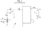
- FIG. 1 shows a conventional transponder 1 which includes an antenna 3 for receiving and transmitting data in the form of radio signals, a means 5 connected to antenna 3 to process data received and the data to be sent, and a means supply 7 to supply a supply voltage Vdd to the various components of transponder 1, in particular through processing 5.
- a so-called "half-duplex" communication between the station basic and the transponder 1 comprises two phases of operation: a reception phase and a phase resignation.
- the base station transmits a radio signal X1, the antenna 3 receives it and converts it into an electrical voltage U 1 .
- the base station can also supply the electrical energy necessary for the electrical supply of the transponder 1, by transmitting the signal X1 at a sufficiently high electrical power.
- the transponder 1 functions as a "passive" component, and the power supply means 7 comprises a storage capacitor intended for storing said electrical energy.
- an electrical voltage U 2 is present at the terminals of the processing means 5, and is supplied to the antenna 3 which converts it into a radio signal X2.
- the capacitor 7 which has stored electrical energy during the reception phase, supplies during the transmission phase the electrical supply necessary for the operation of the processing means. 5.
- a problem encountered during such communication lies in energy optimization electric transferred between the antenna 3 and the means of treatment 5.
- a conventional solution to this problem consists in connecting a capacitor 8 in parallel with the antenna 3, so as to form a parallel LC type circuit, as shown in FIG. 1.
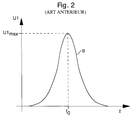
- this circuit can supply the voltage U 1 to a maximum amplitude, when the frequency of this voltage is equal to the resonant frequency fo of this circuit.
- FIG. 2 represents a waveform 9 illustrating the evolution of the voltage U 1 as a function of its frequency f, in the case where the circuit is of the parallel LC type.
- the frequency f of this voltage is substantially equal to said resonant frequency fo, the amplitude of the voltage U1 is maximum, the reference U 1max designating said maximum value of voltage.
- a disadvantage of the conventional solution mentioned above resides in the fact that, during the emission phase, the parallel LC circuit does not allow to optimize the transfer of energy between the means of processing 5 and antenna 3. Indeed, during this phase, if the circuit connected to the terminals of the processing means 5, is of parallel LC type, this means provides a current I2, and the voltage U2 present at limits of said means is limited by its characteristics entry. This results in a limitation of the energy present in antenna 3, as well as magnetic field created by this antenna during the transmission phase.
- An object of the present invention is to provide a transponder overcomes the disadvantages of transponders conventional, in particular to optimize electrical energy exchanged during the reception and transmission phases during a "half-duplex" communication.
- Another object of the present invention is to provide a transponder that meets the criteria traditional in the semiconductor industry, complexity and cost.
- An advantage of the transponder switching means according to the present invention is to realize two different transponder configurations, during reception and transmission phase, suitable for optimizing electrical powers exchanged between the antenna and the means of treatment.
- transponder resides in the fact that it consists of components usually produced in the semiconductor industry, notably by stages of manufacturing a CMOS type die known per se.
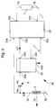
- FIG. 3 represents a transponder 30 according to the present invention.
- transponder 30 shown in Figure 3 has a structure that is close to transponder 1 represented in FIG. 1.
- the components represented in FIG. 3 and designated by the same references as those represented in FIG. 1, are substantially identical to those designated in Figure 1.
- the transponder 30 includes an antenna 3, a capacitor 8, a processing means 33 and a means supply 7.
- the transponder 30 is intended for receive data during the reception phase, and provide other data during the transmission phase.
- the above-mentioned components are arranged and connected as follows.
- the antenna 3 is arranged to be able to receive and transmit radio signals X1 and X2 containing data exchanged between a base station (not shown) and the processing means 33.
- antenna 3 includes two connection terminals 3a and 3b by which are supplied with an electrical voltage U1 containing the data to be processed by the processing means 33, as well as an electrical voltage U2 containing the data to be sent. Furthermore, terminal 3b is connected to the ground of the transponder 30.
- the antenna 3 is produced using a coil, as this is known per se.
- the capacitor 8 is arranged to be able to be connected with the antenna 3.
- the capacitor 8 is includes a first terminal 8a connected to terminal 3a antenna 3, and a second connection terminal 8b.
- Capacitor 8 is produced using a capacitive component, as is known per se.
- the processing means 33 is arranged to be able to receive, process and provide said exchanged data with the antenna 3.
- the processing means 33 includes an input terminal 33a connected with terminal 3a of antenna 3, to receive voltage U1, and a terminal output 33b to supply the voltage U2.
- the processing means 33 includes a power supply terminal 33c to be able to receive a power supply, a ground terminal 33d connected to the ground of the transponder 30, as well as a control terminal 33e to be able to provide a control signal S.
- Processing means 33 are produced by forming a classic logic block and a classic interface arranged between this block and the antenna 3.
- the supply means 7 is arranged to be able to supplying power to the processing means 33, in the form of a supply voltage Vdd.
- the supply means 7 comprises a terminal connection 7a connected to terminal 33c of the means of processing 33, and a ground terminal 7b connected to the mass of the transponder 30.
- the supply means 7 is made in using a storage capacitor for storing the electrical energy transmitted during the phase of reception.
- the supply means 7 is made in using a conventional lithium battery.
- the transponder 30 includes a means of switching 32 which is connected with capacitor 8, the processing means 33 and the mass of this transponder.
- the switching means 32 comprises a first connection terminal 32a connected to terminal 8b of the capacitor 8, a second connection terminal 32b connected to terminal 33b of the processing means 33, and a third connection terminal 32c connected to the ground of the transponder 30.
- the switching means 32 includes a 32d control terminal connected to the terminal 33e of the processing means 33, to receive the signal S.
- the switching means 32 includes two switches 36 and 37 which are connected to the terminal 32d, so that it can be controlled by the signal S.
- the switch 36 is connected between the terminal 32a and terminal 32b, and switch 37 is connected between terminal 32a and terminal 32c.
- the switching means 32 is arranged so as to ability to receive command signal via terminal 32d S supplied by the processing means 33, and connect in response the processing means 33, the capacitor 8, as well as antenna 3, as described so detailed below.
- the means of processing 33 controls the switch 37 when closing, and switch 36 upon opening.
- FIG. 4 shows in detail the transponder 30, during the reception phase, in especially the connections established by means of switching 32.
- transponder of FIG. 4 having the same structure that the transponder of figure 3, the components shown in Figures 3 and 4 are designated by the same references in these two figures.
- the switching means 32 connects terminal 32a to the terminal 32c, so that the antenna 3 is connected in parallel with capacitor 8.
- capacitor 8 and the antenna 3 are connected so as to form a parallel LC type circuit.
- phase reception is followed by the transmission phase.
- processing means 33 controls switch 37 on opening, and switch 36 on closing.
- FIG. 5 shows in detail the transponder 30, during the transmission phase, in especially the connections established by means of switching 32.
- transponder of FIG. 5 having the same structure that the transponder of figure 3, the components shown in Figures 3 and 5 are designated by the same references in these two figures.
- the switching means 32 connects terminal 32b to the terminal 32c, the terminals 32a and 32d being free, so that the antenna 3 is connected in series with the capacitor 8.
- the capacitor 8 and the antenna 3 are connected so as to form a series LC type circuit.
- the capacitor 8 is produced, the means switching 32 and the processing means 33 are made monolithically in a single substrate semiconductor.
- the means switching 32 and the processing means 33 are made monolithically in a single substrate semiconductor.
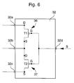
- Figure 6 shows a preferred embodiment switching means 32 which includes two transistors T1 field effect and to form the two respectively switches 36 and 37.
- the substrate is a silicon substrate of P type
- transistor T1 is P type channel
- the transistor T2 is type N channel.
- Each of the transistors T1 and T2 includes a terminal grid, a drain terminal and a source terminal.
- the drain terminal of transistor T1 is connected to terminal 32a, and its source terminal is connected to terminal 32b.
- the source terminal of transistor T2 is connected to the terminal 32c, and its drain terminal is connected to the terminal 32b.
- the gate terminals of the transistors T1 and T2 are connected to terminal 32d, so as to be controlled by the processing means 33, so that the transistor T2 is blocked when transistor T1 is conductive, and conversely, which achieves the two configurations of the transponder 30 described in relation to FIGS. 4 and 5.
- the configuration of the transponder 30 is substantially identical to that of the conventional transponder described in relation to Figures 1 and 2, as already mentioned.
- the station transmits a radio signal X1 to the frequency fo as defined in equation (1).
- the antenna 3 of the transponder 30 converts this signal into the voltage U1 whose frequency is equal to the frequency fo defined above.
- the processing means 33 controls the switching means to connect the antenna 3 and the capacitor 8, to form a parallel LC circuit.
- the LC circuit then realizes a voltage resonance, and the electrical power supplied from antenna 3 by means of 33 treatment is optimal.
- the connected circuit at the terminals of the processing means 33 being of the LC type series, this means provides an electrical voltage U2, unlike the conventional transponder described in relationship to Figure 1, in which the means of treatment 33 provides an electric current I2.
- the current I2 present in the transponder 30 during the issuing phase is not limited.
- the current I2 is supplied at a frequency which is equal to the resonance frequency fo defined above.
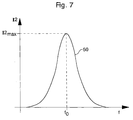
- the FIG. 7 represents a waveform 50 illustrating the relationship between the amplitude and the frequency of said current I2 during an emission phase. So when the frequency f of this current is substantially equal to said resonant frequency fo, the amplitude of the current I2 is maximum.
- the LC series circuit is resonating while running.
- the transponder according to the present invention is particularly advantageous, since configurations of this transponder in reception phase and during the emission phase, optimize the powers electrics exchanged between the antenna and the means of treatment.
Landscapes
- Engineering & Computer Science (AREA)
- Computer Networks & Wireless Communication (AREA)
- Signal Processing (AREA)
- Theoretical Computer Science (AREA)
- Physics & Mathematics (AREA)
- General Physics & Mathematics (AREA)
- Microelectronics & Electronic Packaging (AREA)
- Power Engineering (AREA)
- Computer Hardware Design (AREA)
- Transceivers (AREA)
- Radar Systems Or Details Thereof (AREA)
- Near-Field Transmission Systems (AREA)
- Bidirectional Digital Transmission (AREA)
Abstract
Description
- la figure 1 déjà citée représente un transpondeur selon l'art antérieur;
- la figure 2 déjà citée représente une forme d'onde illustrant la relation entre l'amplitude et la fréquence d'un signal présent dans le transpondeur de la figure 1;
- la figure 3 représente un transpondeur selon la présente invention;
- la figure 4 représente de façon détaillée le transpondeur de la figure 3, au cours d'une phase de réception;
- la figure 5 représente de façon détaillée le transpondeur de la figure 3, au cours d'une phase d'émission;
- la figure 6 représente un mode de réalisation préféré du moyen de commutation du transpondeur de la figure 3;
- la figure 7 représente une forme d'onde illustrant la relation entre l'amplitude et la fréquence d'un signal présent dans le transpondeur de la figure 3, au cours d'une phase d'émission.
Claims (6)
- Transpondeur (30) destiné à recevoir des données au cours d'une première phase ou phase de réception, et fournir d'autres données au cours d'une seconde phase ou phase d'émission, ce transpondeur comprenant :ce transpondeur étant caractérisé en ce qu'il comprend en outre un moyen de commutation (32) connecté avec le condensateur et le moyen de traitement, et agencé de sorte que, sous la commande du moyen de traitement, le moyen de commutation peut connecter le moyen de traitement en série avec le condensateur et la bobine qui sont eux-mêmes connectés pour former, pendant toute la durée de la phase de réception, un circuit de type LC parallèle et, pendant toute la durée de la phase d'émission, un circuit de type LC série.une bobine (3) agencée en tant qu'antenne pour pouvoir recevoir et émettre des signaux radioélectriques contenant lesdites données;un condensateur (8) connecté à la bobine, pour former un circuit résonant;un moyen de traitement (33) agencé pour pouvoir recevoir, traiter et fournir lesdites données; etun moyen d'alimentation (7) connecté au moyen de traitement, et agencé pour pouvoir fournir un signal d'alimentation électrique à différents composants du transpondeur,
- Transpondeur (30) selon la revendication 1, caractérisé en ce que la bobine (3), le condensateur (8), le moyen de commutation (32) et le moyen de traitement (33) sont réalisés de façon monolithique dans un unique substrat semiconducteur.
- Transpondeur (30) selon la revendication 2, caractérisé en ce que l'antenne (3) est réalisée de façon monolithique dans ledit substrat.
- Transpondeur (30) selon la revendication 2 ou 3, caractérisé en ce que le moyen de commutation (32) comprend :un premier transistor (37) qui est à effet de champ et à canal de type N; etun second transistor (36) qui est à effet de champ et à canal de type P.
- Transpondeur (30) selon la revendication 2 ou 3, caractérisé en ce que le moyen de commutation (32) comprend :un premier transistor (37) qui est à effet de champ et à canal de type P; etun second transistor (36) qui est à effet de champ et à canal de type N.
- Transpondeur (30) selon la revendication 4 ou 5, caractérisé en ce que les premier et second transistors (36; 37) sont commandés par le moyen de traitement (33).
Priority Applications (3)
| Application Number | Priority Date | Filing Date | Title |
|---|---|---|---|
| DE69733201T DE69733201T2 (de) | 1997-12-23 | 1997-12-23 | Transponder für "Halbduplex"-Kommunikation |
| EP97122711A EP0926855B1 (fr) | 1997-12-23 | 1997-12-23 | Transpondeur pour communication dite "half-duplex" |
| AT97122711T ATE295028T1 (de) | 1997-12-23 | 1997-12-23 | TRANSPONDER FÜR ßHALF DUPLEXß-KOMMUNIKATION |
Applications Claiming Priority (1)
| Application Number | Priority Date | Filing Date | Title |
|---|---|---|---|
| EP97122711A EP0926855B1 (fr) | 1997-12-23 | 1997-12-23 | Transpondeur pour communication dite "half-duplex" |
Publications (2)
| Publication Number | Publication Date |
|---|---|
| EP0926855A1 true EP0926855A1 (fr) | 1999-06-30 |
| EP0926855B1 EP0926855B1 (fr) | 2005-05-04 |
Family
ID=8227859
Family Applications (1)
| Application Number | Title | Priority Date | Filing Date |
|---|---|---|---|
| EP97122711A Expired - Lifetime EP0926855B1 (fr) | 1997-12-23 | 1997-12-23 | Transpondeur pour communication dite "half-duplex" |
Country Status (3)
| Country | Link |
|---|---|
| EP (1) | EP0926855B1 (fr) |
| AT (1) | ATE295028T1 (fr) |
| DE (1) | DE69733201T2 (fr) |
Cited By (2)
| Publication number | Priority date | Publication date | Assignee | Title |
|---|---|---|---|---|
| WO2005055654A1 (fr) * | 2003-11-26 | 2005-06-16 | Starkey Laboratories, Inc. | Commutation emission-reception dans des protheses auditives sans fil |
| WO2012140169A1 (fr) | 2011-04-15 | 2012-10-18 | Gemalto Sa | Procede, circuit et dispositif de communication sans contact a emission activee |
Citations (3)
| Publication number | Priority date | Publication date | Assignee | Title |
|---|---|---|---|---|
| US5517179A (en) * | 1995-05-18 | 1996-05-14 | Xlink Enterprises, Inc. | Signal-powered frequency-dividing transponder |
| WO1996028880A2 (fr) * | 1995-03-16 | 1996-09-19 | British Technology Group Inter-Corporate Licensing Limited | Transpondeur pour systeme d'identification electronique |
| EP0777193A1 (fr) * | 1995-12-01 | 1997-06-04 | RAIMBAULT, Pierre | Circuit d'alimentation et de modulation pour une étiquette interrogeable à distance |
-
1997
- 1997-12-23 DE DE69733201T patent/DE69733201T2/de not_active Expired - Lifetime
- 1997-12-23 EP EP97122711A patent/EP0926855B1/fr not_active Expired - Lifetime
- 1997-12-23 AT AT97122711T patent/ATE295028T1/de not_active IP Right Cessation
Patent Citations (3)
| Publication number | Priority date | Publication date | Assignee | Title |
|---|---|---|---|---|
| WO1996028880A2 (fr) * | 1995-03-16 | 1996-09-19 | British Technology Group Inter-Corporate Licensing Limited | Transpondeur pour systeme d'identification electronique |
| US5517179A (en) * | 1995-05-18 | 1996-05-14 | Xlink Enterprises, Inc. | Signal-powered frequency-dividing transponder |
| EP0777193A1 (fr) * | 1995-12-01 | 1997-06-04 | RAIMBAULT, Pierre | Circuit d'alimentation et de modulation pour une étiquette interrogeable à distance |
Cited By (4)
| Publication number | Priority date | Publication date | Assignee | Title |
|---|---|---|---|---|
| WO2005055654A1 (fr) * | 2003-11-26 | 2005-06-16 | Starkey Laboratories, Inc. | Commutation emission-reception dans des protheses auditives sans fil |
| US7512383B2 (en) | 2003-11-26 | 2009-03-31 | Starkey Laboratories, Inc. | Transmit-receive switching in wireless hearing aids |
| WO2012140169A1 (fr) | 2011-04-15 | 2012-10-18 | Gemalto Sa | Procede, circuit et dispositif de communication sans contact a emission activee |
| US9800300B2 (en) | 2011-04-15 | 2017-10-24 | Gemalto Sa | Method, circuit and contactless communication device with activated emitting |
Also Published As
| Publication number | Publication date |
|---|---|
| DE69733201D1 (de) | 2005-06-09 |
| EP0926855B1 (fr) | 2005-05-04 |
| ATE295028T1 (de) | 2005-05-15 |
| DE69733201T2 (de) | 2006-01-26 |
Similar Documents
| Publication | Publication Date | Title |
|---|---|---|
| EP0999517B1 (fr) | Transpondeur actif rechargeable | |
| EP1617550B1 (fr) | Circuit d'alimentation adaptable | |
| JP4463891B2 (ja) | トランスポンダ | |
| EP0836271B1 (fr) | Oscillateur intégré et radio-téléphone mettant en oeuvre un tel oscillateur. | |
| FR2942365A1 (fr) | Dispositif de communication incluant une batterie et un module de communication a champ proche | |
| EP0720292A1 (fr) | Dispositif terminal mobile pour télécommunication incluant un circuit commutateur | |
| EP1172929A1 (fr) | Dispositif d'amplification à faible bruit, en particulier pour un téléphone mobile cellulaire | |
| EP0638160B1 (fr) | Dispositif de deminage | |
| EP0586285B1 (fr) | Tête optique d'émission-réception pour transmission de données par système optique, et circuit de commutation pour cette tête | |
| EP0926855B1 (fr) | Transpondeur pour communication dite "half-duplex" | |
| EP1040447B1 (fr) | Transpondeur actif commutable en transpondeur passif | |
| EP0755114B1 (fr) | Dispositif semi-conducteur incluant un amplificateur de puissance et appareil terminal mobile de télécommunication incluant un tel dispositif semi-conducteur | |
| EP2810334A1 (fr) | Systeme de communication dans une batterie electrique | |
| FR2829653A1 (fr) | Dispositif d'alimentation a decoupage adapte pour les faibles consommations de courant, et telephone cellulaire dote d'un tel dispositif | |
| EP0005096A1 (fr) | Source d'ondes millimétriques | |
| EP3648362A1 (fr) | Procédé de limitation du niveau de tension issue d'un champ magnétique reçu par un transpondeur et transpondeur correspondant | |
| EP4059160B1 (fr) | Dispositif de communication optique sans fil | |
| FR2787260A1 (fr) | Dispositif electronique de communication sans contact a source d'energie auxiliaire optionnelle | |
| EP1039652B1 (fr) | Arrangement d'antenne | |
| FR2904132A1 (fr) | Dispositif d'identification par radiofrequence (rfid) appose sur un objet a identifier | |
| FR3062937A1 (fr) | Activation d'un dispositif nfc | |
| EP0061421A1 (fr) | Circuit intégré pour oscillateur à fréquence réglable | |
| EP0712059A1 (fr) | Circuit de commande d'un vibreur piézo-électrique | |
| EP4668593A1 (fr) | Dispositif electronique a liaison sans fil | |
| WO2002047283A1 (fr) | Tete d'emission-reception |
Legal Events
| Date | Code | Title | Description |
|---|---|---|---|
| PUAI | Public reference made under article 153(3) epc to a published international application that has entered the european phase |
Free format text: ORIGINAL CODE: 0009012 |
|
| AK | Designated contracting states |
Kind code of ref document: A1 Designated state(s): AT BE CH DE FR GB IE LI NL |
|
| AX | Request for extension of the european patent |
Free format text: AL;LT;LV;MK;RO;SI |
|
| 17P | Request for examination filed |
Effective date: 19991230 |
|
| AKX | Designation fees paid |
Free format text: AT BE CH DE FR GB IE LI NL |
|
| 17Q | First examination report despatched |
Effective date: 20040302 |
|
| GRAP | Despatch of communication of intention to grant a patent |
Free format text: ORIGINAL CODE: EPIDOSNIGR1 |
|
| GRAS | Grant fee paid |
Free format text: ORIGINAL CODE: EPIDOSNIGR3 |
|
| GRAA | (expected) grant |
Free format text: ORIGINAL CODE: 0009210 |
|
| AK | Designated contracting states |
Kind code of ref document: B1 Designated state(s): AT BE CH DE FR GB IE LI NL |
|
| PG25 | Lapsed in a contracting state [announced via postgrant information from national office to epo] |
Ref country code: NL Free format text: LAPSE BECAUSE OF FAILURE TO SUBMIT A TRANSLATION OF THE DESCRIPTION OR TO PAY THE FEE WITHIN THE PRESCRIBED TIME-LIMIT Effective date: 20050504 Ref country code: IE Free format text: LAPSE BECAUSE OF FAILURE TO SUBMIT A TRANSLATION OF THE DESCRIPTION OR TO PAY THE FEE WITHIN THE PRESCRIBED TIME-LIMIT Effective date: 20050504 Ref country code: AT Free format text: LAPSE BECAUSE OF FAILURE TO SUBMIT A TRANSLATION OF THE DESCRIPTION OR TO PAY THE FEE WITHIN THE PRESCRIBED TIME-LIMIT Effective date: 20050504 |
|
| REG | Reference to a national code |
Ref country code: GB Ref legal event code: FG4D Free format text: NOT ENGLISH |
|
| REG | Reference to a national code |
Ref country code: CH Ref legal event code: EP |
|
| REG | Reference to a national code |
Ref country code: IE Ref legal event code: FG4D Free format text: LANGUAGE OF EP DOCUMENT: FRENCH |
|
| REF | Corresponds to: |
Ref document number: 69733201 Country of ref document: DE Date of ref document: 20050609 Kind code of ref document: P |
|
| REG | Reference to a national code |
Ref country code: CH Ref legal event code: NV Representative=s name: ICB INGENIEURS CONSEILS EN BREVETS SA |
|
| GBT | Gb: translation of ep patent filed (gb section 77(6)(a)/1977) |
Effective date: 20050817 |
|
| NLV1 | Nl: lapsed or annulled due to failure to fulfill the requirements of art. 29p and 29m of the patents act | ||
| REG | Reference to a national code |
Ref country code: IE Ref legal event code: FD4D |
|
| PG25 | Lapsed in a contracting state [announced via postgrant information from national office to epo] |
Ref country code: BE Free format text: LAPSE BECAUSE OF NON-PAYMENT OF DUE FEES Effective date: 20051231 |
|
| PLBE | No opposition filed within time limit |
Free format text: ORIGINAL CODE: 0009261 |
|
| STAA | Information on the status of an ep patent application or granted ep patent |
Free format text: STATUS: NO OPPOSITION FILED WITHIN TIME LIMIT |
|
| 26N | No opposition filed |
Effective date: 20060207 |
|
| BERE | Be: lapsed |
Owner name: EM MICROELECTRONIC-MARIN SA Effective date: 20051231 |
|
| PGFP | Annual fee paid to national office [announced via postgrant information from national office to epo] |
Ref country code: GB Payment date: 20101201 Year of fee payment: 14 |
|
| GBPC | Gb: european patent ceased through non-payment of renewal fee |
Effective date: 20121223 |
|
| PG25 | Lapsed in a contracting state [announced via postgrant information from national office to epo] |
Ref country code: GB Free format text: LAPSE BECAUSE OF NON-PAYMENT OF DUE FEES Effective date: 20121223 |
|
| PGFP | Annual fee paid to national office [announced via postgrant information from national office to epo] |
Ref country code: DE Payment date: 20131121 Year of fee payment: 17 Ref country code: CH Payment date: 20131125 Year of fee payment: 17 |
|
| PGFP | Annual fee paid to national office [announced via postgrant information from national office to epo] |
Ref country code: FR Payment date: 20131219 Year of fee payment: 17 |
|
| REG | Reference to a national code |
Ref country code: DE Ref legal event code: R119 Ref document number: 69733201 Country of ref document: DE |
|
| REG | Reference to a national code |
Ref country code: CH Ref legal event code: PL |
|
| REG | Reference to a national code |
Ref country code: FR Ref legal event code: ST Effective date: 20150831 |
|
| PG25 | Lapsed in a contracting state [announced via postgrant information from national office to epo] |
Ref country code: DE Free format text: LAPSE BECAUSE OF NON-PAYMENT OF DUE FEES Effective date: 20150701 Ref country code: LI Free format text: LAPSE BECAUSE OF NON-PAYMENT OF DUE FEES Effective date: 20141231 Ref country code: CH Free format text: LAPSE BECAUSE OF NON-PAYMENT OF DUE FEES Effective date: 20141231 |
|
| PG25 | Lapsed in a contracting state [announced via postgrant information from national office to epo] |
Ref country code: FR Free format text: LAPSE BECAUSE OF NON-PAYMENT OF DUE FEES Effective date: 20141231 |