EP0926598B1 - A field programmable gate array with integrated debugging facilities - Google Patents
A field programmable gate array with integrated debugging facilities Download PDFInfo
- Publication number
- EP0926598B1 EP0926598B1 EP19970122571 EP97122571A EP0926598B1 EP 0926598 B1 EP0926598 B1 EP 0926598B1 EP 19970122571 EP19970122571 EP 19970122571 EP 97122571 A EP97122571 A EP 97122571A EP 0926598 B1 EP0926598 B1 EP 0926598B1
- Authority
- EP
- European Patent Office
- Prior art keywords
- les
- integrated circuit
- selector
- signal
- coupled
- Prior art date
- Legal status (The legal status is an assumption and is not a legal conclusion. Google has not performed a legal analysis and makes no representation as to the accuracy of the status listed.)
- Expired - Lifetime
Links
- 230000004044 response Effects 0.000 claims description 9
- 239000000872 buffer Substances 0.000 claims description 4
- 238000013461 design Methods 0.000 abstract description 13
- 238000013507 mapping Methods 0.000 description 3
- 238000012360 testing method Methods 0.000 description 3
- 101150055297 SET1 gene Proteins 0.000 description 2
- 230000000295 complement effect Effects 0.000 description 2
- 230000004075 alteration Effects 0.000 description 1
- 230000008878 coupling Effects 0.000 description 1
- 238000010168 coupling process Methods 0.000 description 1
- 238000005859 coupling reaction Methods 0.000 description 1
- 238000010586 diagram Methods 0.000 description 1
- 230000008014 freezing Effects 0.000 description 1
- 238000007710 freezing Methods 0.000 description 1
- 239000000463 material Substances 0.000 description 1
- 238000000034 method Methods 0.000 description 1
- 238000012986 modification Methods 0.000 description 1
- 230000004048 modification Effects 0.000 description 1
Images


Classifications
-
- G—PHYSICS
- G01—MEASURING; TESTING
- G01R—MEASURING ELECTRIC VARIABLES; MEASURING MAGNETIC VARIABLES
- G01R31/00—Arrangements for testing electric properties; Arrangements for locating electric faults; Arrangements for electrical testing characterised by what is being tested not provided for elsewhere
- G01R31/28—Testing of electronic circuits, e.g. by signal tracer
- G01R31/317—Testing of digital circuits
- G01R31/3181—Functional testing
- G01R31/3185—Reconfiguring for testing, e.g. LSSD, partitioning
- G01R31/318516—Test of programmable logic devices [PLDs]
- G01R31/318519—Test of field programmable gate arrays [FPGA]
-
- G—PHYSICS
- G01—MEASURING; TESTING
- G01R—MEASURING ELECTRIC VARIABLES; MEASURING MAGNETIC VARIABLES
- G01R31/00—Arrangements for testing electric properties; Arrangements for locating electric faults; Arrangements for electrical testing characterised by what is being tested not provided for elsewhere
- G01R31/28—Testing of electronic circuits, e.g. by signal tracer
- G01R31/317—Testing of digital circuits
- G01R31/31705—Debugging aspects, e.g. using test circuits for debugging, using dedicated debugging test circuits
-
- G—PHYSICS
- G01—MEASURING; TESTING
- G01R—MEASURING ELECTRIC VARIABLES; MEASURING MAGNETIC VARIABLES
- G01R31/00—Arrangements for testing electric properties; Arrangements for locating electric faults; Arrangements for electrical testing characterised by what is being tested not provided for elsewhere
- G01R31/28—Testing of electronic circuits, e.g. by signal tracer
- G01R31/317—Testing of digital circuits
- G01R31/3181—Functional testing
- G01R31/3185—Reconfiguring for testing, e.g. LSSD, partitioning
- G01R31/318533—Reconfiguring for testing, e.g. LSSD, partitioning using scanning techniques, e.g. LSSD, Boundary Scan, JTAG
- G01R31/318536—Scan chain arrangements, e.g. connections, test bus, analog signals
Definitions
- the present invention relates to the fields of field programmable gate array (FPGA) and emulation systems.
- FPGA field programmable gate array
- Emulation systems for emulating circuit design are known in the art. Typically, prior art emulation systems are formed using general purpose FPGAs without integrated debugging facilities. A circuit design to be emulated is "realized” on the emulation system by compiling a “formal” description of the circuit design, and mapping the circuit design onto the logic elements (LEs) of the FPGAs.
- Ls logic elements
- US-A-5 425 036 describes an emulation system using FPGAs wherein the logic elements of the FPGAs incorporate a D flip-flop which may be utilized to hold the output signal of the logic element on demand.
- the FPGAs are additionally provided with boundary scan test logic incorporating built-in self-test which complies with all the relevant specifications given in the IEEE Standard 1149.1 (PROC. FIFTH GREAT LAKES SYMPOSIUM ON VLSI, 16-18 March 1995, pages 242-246, IEEE Computer Society Press, Los Alamitos, CA, US; POTTINGER, H. J. et al.: "Using a reconfigurable field programmable gate array to demonstrate boundary scan with built in self test").
- the FPGAs if specifically configured, enable initialization of the D flip-flops in the LEs. Reconfiguration is, however, necessary after initialization to implement the operational circuit to be emulated. Thus, it is desirable to have an improved FPGA with integrated debugging facilities that is more suitable for usage by the emulation systems in that the need to reconfigure the circuitry from initialization to the operational circuit is eliminated.
- the Improved FPGA comprises a number of enhanced logic elements (LEs) interconnected to each other, preferably, via a network of crossbars.
- Each enhanced LE comprises a multiple input-single output truth table and a complementary pair of master-slave latches having a data, a set and a reset input, and control logic.
- the enhanced LE may be used for "level sensitive” as well as "edge sensitive” circuit design emulations.
- Each enhanced LE further comprises a plurality of multiplexors and buffers, allowing each LE to be individually initialized, its state to be frozen momentarily, and the frozen state to be read or modified.
- the improved FPGA further comprises a complementary context bus and read/write facilities for setting the enhanced LEs' initial values, and for reading of their frozen states.
- the improved FPGA also comprises a scan register for outputting trace data for the enhanced LEs.
- the improved FPGA also comprises a plurality of trigger circuitry for conditionally generating a plurality of trigger inputs.
- FPGA 100 which is disposed on a single integrated circuit (or chip), comprises an array 102 of enhanced LEs incorporated with the teachings of the present invention.
- the enhanced LEs are used to "realize" various elements of circuit designs, however, as will be disclosed in more detail below, unlike the prior art, the enhanced LEs include new and innovative debugging features.
- FPGA 100 further advantageously includes on-chip context bus 106, scan register 108 and trigger circuitry 110, coupled to the enhanced LEs as shown.
- context bus 106 is used for inputting and outputting values to and from the LEs
- scan register 108 and trigger circuitry 110 are used to output trace data and trigger inputs for FPGA 100 respectively.
- FPGA 100 includes memory 112 to facilitate usage of FPGA 100 for emulating circuit designs with memory.
- memory 112 is 16-bit wide.
- the pins 113 of FPGA 100 can be used for either input or output.
- 64 I/O pins 113 are provided to FPGA 100.
- FPGA 100 also includes inter-LE crossbar (or x-bar) network 104 for interconnecting the LEs, memory 112, and I/O pins 113, as shown.
- FPGA 100 it is also preferable for FPGA 100 to include "two copies" of the first stage of a crossbar network 114a - 114b for inter-connecting FPGA 100 to other FPGAs and a "host system".
- Inter-LE crossbar network 104 and the first stage of inter-FPGA crossbar network 114a will be briefly described below. LEs, context bus 106, scan register 108, and trigger circuitry 110 will be described in further detail below with additional references to the remaining figures.
- FIG. 2 illustrates one embodiment of the array of enhanced LEs of Fig.1 and one embodiment of the LEs themselves in further detail.
- LE array 102 comprises a plurality of enhanced LEs 200 of the present invention.
- LE array 102 comprises 128 LEs 200.
- Each LE 200 includes a multiple input - single output truth table 202, a pair of master-slave latches 204- 206, output multiplexor 208, input multiplexor 210, and control logic 212, coupled to each other as shown.
- Truth table 202 is used to generate a predetermined output in response to a set of inputs.
- truth-table 202 has 4 inputs and 1 output. In other words, depending on the inputs, truth table 202 outputs 1 of 2 4 of predetermined outputs.
- Each of master-slave latches 204 - 206 is used to store an input value synchronously with its clock input. Furthermore, each of master-slave latches 204 - 206 can be asynchronously forced to one or zero depending on the values of set and reset.
- the set and reset inputs are provided using the inputs I3 and I2 of truth table 202.
- Output multiplexor 208, input multiplexor 210 and control logic 212 are used to control the manner in which truth table 202 and master-slave latches 204 - 206 are used.
- Output multiplexor 208 allows either the output of truth table 202 (bypassing master-slave latches 204 - 206) or the output of slave latch 206 (for level sensitive designs), or the output of master latch 204 (for edge sensitive designs) to be selected for output. The by-passed output is selected if truth table 202 is to be used standalone.
- input multiplexor 210 allows either the output of truth table 202, the feedback from output multiplexor 208, or an input value on context bus 106 to be provided to master-slave latches 204 - 206.
- the feedback value is selected to "freeze" LE 200, and the bus value is selected to initialize LE 200 .
- Control logic 212 controls input multiplexor 210 and the set and reset values provided to master-slave latches 204 - 206, in accordance to a set, a reset, a first and a second enable (ENAB and EN), a load (LDE) and a hold (HLD) value provided, to be described more fully below.
- Each LE 200 also includes clock selection multiplexors 216a - 216c for selectively providing a number of emulation clocks or a debug clock (LD) to master-slave latches 204 - 206.
- the emulation clocks include a "constructed" emulation clock using other LEs 200.
- this "constructed" emulation clock is made available through I0 of truth table 202.
- One of the emulation clocks is provided to master-slave latches 204 - 206 during normal operation, whereas the debug clock (LD) is provided during debugging.
- the clock selection is controlled by the CTX signal.
- LE 200 also includes buffer 214a for outputting the selected output to inter-LE X-bar network 104 and the on-chip debugging facilities, and buffer 214b for outputting the selected output onto context bus 106 for direct observation outside FPGA 100.
- truth table 202 may be used in a standalone manner, or in conjunction with the corresponding master-slave latches 204 - 206.
- Enhanced LE 200 is suitable for "level sensitive” as well as “edge sensitive” circuit design emulations.
- each LE 200 can be individually initialized.
- Each LE 200 can also be caused to output the same output over and over again, as if it is frozen.
- LEs 200 are individually and directly observable outside FPGA 100. In other words, there are no "hidden nodes”. The state of each "node” is directly observable outside the FPGA, without requiring the reconfiguration and time consuming re-compilation of circuit design mappings normally performed under the prior art.
- FIG. 3 illustrates one embodiment each of input multiplexor 210 and control logic 212 in further detail.
- multiplexor 210 comprises drivers 211a - 211c for outputting the feedback output, the output of truth-table 202, and the input value on context bus 106 respectively, if enabled.
- One of drivers 211a - 211c is selectively enabled by control signals from control logic 212 .
- Control logic 212 comprises AND gates 213a - 213c, OR gate 215, NOR gate 217, and memory bits 219a - 219c for generating the control signals for driver 211a - 211c, as well as the set and reset values for master-slave latches 204 - 206.
- Memory bits 219a - 219c are used to store configuration information for enabling the provision of the set and reset values and the selection of the feedback output. If enabled, AND gates 213a - 213b provides the set and reset values in accordance to the set and HLD inputs, and the reset and HLD inputs respectively. If enabled, OR gate 215 in conjunction with AND gate 213c provide the control signal for driver 211a in accordance to the ENAB, HLD and EN inputs. NOR gate 217 provide the control signal for driver 211b in accordance to the control signal being provided for driver 211a and a LDE input. Lastly, the LDE input is provided as the control signal for driver 211c.
- inter-LE crossbar network 104 for interconnecting the LEs, the memory and the I/O pins is illustrated.
- inter-LE crossbar network 104 comprises 4 subnetworks 220.
- the first two subnetworks, subnet0 and subnet1 are used to route 72 signals, whereas the remaining two subnetworks, subnet2 and subnet3, are used to route 64 signals.
- Subnet0 is used to route the signals of LE0 - LE39, LE119 - LE127, I/O0 - I/O15 and M0 - M7.
- Subnet1 is used to route the signals of LE24 - LE71, I/O16 - I/O31 and M8 - M15.
- Subnet2 is used to route the signals of LE56 - LE103, and I/O32 - I/O47.
- Subnet3 is used to route the signals of LE0 - LE7, LE88 - LE127, and I/O48 - I/O63. The overlapping coverage of the LEs provides increased flexibility of signal routing for mapping circuit designs.
- Each subnetwork 220 is a three-stage Claus network comprising either 9 or 8 8-to-8 crossbars 222 in the first stage, 8 9-to-20 or 8-to-20 crossbars 224 or 226 in stage two, and 20 8-to-8 crossbars 228 in stage three.
- the stages are coupled to each other in the well known "butterfly" manner.
- inter-FPGA crossbar network stage0 114a - 114b for interconnecting the FPGA to other FPGAs and a "host" computer is illustrated.
- inter-FPGA crossbar network stage0 114a - 114b comprises 4 pairs of 16-to-16 crossbars 230 for coupling 64 I/O signals of the FPGA to the next stage of a Claus network for interconnecting the FPGA to other FPGAs and a "host" computer.
- Figure 6 illustrates one embodiment of the read/write facilities associated with context bus 106 for reading from and writing into LEs 200 of FPGA 100.
- 128 LEs 200 are organized in 16 columns, with each column having 8 LEs 200.
- Address register 232 is provided for storing the read or write address.
- Decoder 234 is provided for decoding the read or write address, which in conjunction with R/W control 236 provide the appropriate read control signals (RD0 - RD15) and write control signals (LDE0 - LDE15) for the 128 LEs 200.
- each LE 200 receives the earlier described HLD signal for "freezing" the LEs 200, the CTX signal for selecting the debug (LD) clock, and the LD clock itself.
- Figures 7a - 7b illustrate exemplary signal timings for reading and writing.
- context reading is done by first loading a 4-bit address into address register 232.
- decoder 234 causes R/W control 236 to drive the appropriate RD signals high to read out the contents of the addressed LEs 200. (HLD, CTX, LDEi and LD all remain low while a read operation is in progress.)
- context writing is done by first loading a 4-bit address into address register 232. Additionally, before decoder 234 responds and causes R/W control 236 to drive the appropriate LDE signals high, HLD is first driven high to freeze all LEs 200.
- CTX is driven high to select debug clock LD for each LE 200.
- R/W control 236 drives the appropriate LDE signals
- values on context bus 106 are loaded into the addressed LEs 200. It is important to freeze all LEs 200 during a context writing, because partial context could induce temporary states, which could in turn put an emulation system into an unknown state. For example, the final context may drive a given RESET signal to the low state, but the partial context (during the writing operation) may induce a temporary high state on the RESET signal, thus unpredictably resetting all the latches connected to the signal.
- Figure 8 illustrates one embodiment of scan register 108 for outputting trace data.
- scan register 108 comprises 16 sets of 8 flip-flops 242, and 15 sets of 8 multiplexors 244, disposed in between flip-flop sets 242.
- Flip-flop set0 242 is coupled to a first group of 8 LEs 200.
- Multiplexor set0 244 is coupled to flip-flop set0 242 and a second group of LEs 200.
- Flip-flop set1 242 is coupled to multiplexor set0, and so forth.
- Flip-flop set0 242 sequentially receives and propagates the outputs of the first group of 8 LEs 200.
- Multiplexor set0 242 either serially provides the outputs of flip-flop set0 242 or the outputs of the second group of 8 LEs.
- Flip-flop set1 242 in turn sequentially propagates the inputs it received from multiplexor set0 244.
- Flip-flop sets 242 are controlled by a scan clock, whereas, multiplexor sets 244 are controlled by a scan control signal.
- a scan clock having the appropriate divided frequency relative to the operating emulation clock
- selectively applying the appropriate scan control signal to the multiplexor sets 244 a snapshot of 128 LEs at a particular clock cycle can be sequentially scanned out of FPGA 100.
- FIG. 9 illustrates one embodiment of trigger circuitry 110 for outputting trigger inputs.
- trigger circuitry 110 comprises 4 comparator-register circuits 260 for generating 4 trigger inputs, one from each comparator-register circuit 260.
- Each comparator-register circuit 260 includes a register 262 for storing a signal pattern, and an equality comparator 264 for comparing the outputs of the LEs to the stored content of pattern register 262.
- the signal pattern comprises 2-bits per LE 200, allowing the values of High, Low, or Don't Care to be encoded.
- An input to a trigger outside FPGA 100 is generated whenever the stored pattern is detected.
- 4 LE internal state events can be monitored simultaneously.
Landscapes
- Engineering & Computer Science (AREA)
- General Engineering & Computer Science (AREA)
- Physics & Mathematics (AREA)
- General Physics & Mathematics (AREA)
- Logic Circuits (AREA)
- Debugging And Monitoring (AREA)
- Test And Diagnosis Of Digital Computers (AREA)
Abstract
Description
- The present invention relates to the fields of field programmable gate array (FPGA) and emulation systems.
- Emulation systems for emulating circuit design are known in the art. Typically, prior art emulation systems are formed using general purpose FPGAs without integrated debugging facilities. A circuit design to be emulated is "realized" on the emulation system by compiling a "formal" description of the circuit design, and mapping the circuit design onto the logic elements (LEs) of the FPGAs.
- These general purpose FPGAs, as far as their applications to emulation systems are concerned, have a number of disadvantages. First of all, the states of signals at the nodes mapped inside the FPGAs are not directly observable, thus the term "hidden" nodes. Secondly, in order to be able to observe the states of signals at these "hidden" nodes, reconfiguration, and therefore extremely time consuming recompilation is required to bring these signals outside the FPGAs to a logic analyzer. Thirdly, a number of the FPGA I/Os will have to be consumed for bringing these signals to the logic analyzer. Furthermore, the additional signals to be routed further increase signal routing congestion. Finally, for timing sensitive applications, it is difficult to know whether the signals at these "hidden" nodes were read at precisely the correct time or not, if the signals are to be read in response to the occurrence of certain events, since the signals have to be brought out of the FPGAs before the read triggering events can be detected.
- US-A-5 425 036 describes an emulation system using FPGAs wherein the logic elements of the FPGAs incorporate a D flip-flop which may be utilized to hold the output signal of the logic element on demand. The FPGAs are additionally provided with boundary scan test logic incorporating built-in self-test which complies with all the relevant specifications given in the IEEE Standard 1149.1 (PROC. FIFTH GREAT LAKES SYMPOSIUM ON VLSI, 16-18 March 1995, pages 242-246, IEEE Computer Society Press, Los Alamitos, CA, US; POTTINGER, H. J. et al.: "Using a reconfigurable field programmable gate array to demonstrate boundary scan with built in self test"). The FPGAs, if specifically configured, enable initialization of the D flip-flops in the LEs. Reconfiguration is, however, necessary after initialization to implement the operational circuit to be emulated. Thus, it is desirable to have an improved FPGA with integrated debugging facilities that is more suitable for usage by the emulation systems in that the need to reconfigure the circuitry from initialization to the operational circuit is eliminated.
- This is attained in the present invention as defined in
claim 1. - The Improved FPGA according to the present invention comprises a number of enhanced logic elements (LEs) interconnected to each other, preferably, via a network of crossbars. Each enhanced LE comprises a multiple input-single output truth table and a complementary pair of master-slave latches having a data, a set and a reset input, and control logic. As a result, the enhanced LE may be used for "level sensitive" as well as "edge sensitive" circuit design emulations. Each enhanced LE further comprises a plurality of multiplexors and buffers, allowing each LE to be individually initialized, its state to be frozen momentarily, and the frozen state to be read or modified. Additionally, the improved FPGA further comprises a complementary context bus and read/write facilities for setting the enhanced LEs' initial values, and for reading of their frozen states. The improved FPGA also comprises a scan register for outputting trace data for the enhanced LEs. Lastly, the improved FPGA also comprises a plurality of trigger circuitry for conditionally generating a plurality of trigger inputs.
- The present invention will be described by way of exemplary embodiments, but not limitations, illustrated in the accompanying drawings in which like references denote similar elements, and in which:
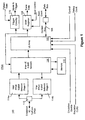
- Figure 1 illustrates the major functional blocks of the FPGA of the present invention;
- Figure 2 illustrates one embodiment of the LE array of Fig. 1, and one embodiment of the enhanced LE;
- Figure 3 illustrates one embodiment each of the control logic and input selector for the master-slave latches of Fig. 1;
- Figures 4a - 4b illustrate one embodiment of the inter-LE crossbar network of Fig. 1
- Figure 5 illustrates one embodiment of the inter-FPGA crossbar network stage0 of Fig. 1;
- Figure 6 illustrates one embodiment of the associated read/write facilities of the context bus of Fig. 1;
- Figures 7a - 7b are two exemplary timing diagrams illustrating the reading of a value from a LE and the writing of a value into a LE;
- Figure 8 illustrates one embodiment of the scan register of Fig. 1; and
- Figure 9 illustrates one embodiment of the trigger circuitry of Fig. 1.
-
- In the following description, for purposes of explanation, specific numbers, materials and configurations are set forth in order to provide a thorough understanding of the present invention. However, it will be apparent to one skilled in the art that the present invention may be practiced without the specific details. In other instances, well known features are omitted or simplified in order not to obscure the present invention.
- Referring now to Figure 1, the major functional blocks of improved
FPGA 100 of the present invention are illustrated. As shown,FPGA 100, which is disposed on a single integrated circuit (or chip), comprises anarray 102 of enhanced LEs incorporated with the teachings of the present invention. As in the prior art, the enhanced LEs are used to "realize" various elements of circuit designs, however, as will be disclosed in more detail below, unlike the prior art, the enhanced LEs include new and innovative debugging features. - Additionally, FPGA 100 further advantageously includes on-
chip context bus 106,scan register 108 andtrigger circuitry 110, coupled to the enhanced LEs as shown. As will be disclosed in more detail below,context bus 106 is used for inputting and outputting values to and from the LEs, whereasscan register 108 andtrigger circuitry 110 are used to output trace data and trigger inputs forFPGA 100 respectively. - Preferably, FPGA 100 includes
memory 112 to facilitate usage ofFPGA 100 for emulating circuit designs with memory. In one embodiment,memory 112 is 16-bit wide. Preferably, thepins 113 ofFPGA 100 can be used for either input or output. In one embodiment, 64 I/O pins 113 are provided toFPGA 100. Preferably,FPGA 100 also includes inter-LE crossbar (or x-bar)network 104 for interconnecting the LEs,memory 112, and I/O pins 113, as shown. Finally, it is also preferable forFPGA 100 to include "two copies" of the first stage of acrossbar network 114a - 114b forinter-connecting FPGA 100 to other FPGAs and a "host system". -
Memory 112 is well known in the art and will not be further described.Inter-LE crossbar network 104 and the first stage ofinter-FPGA crossbar network 114a will be briefly described below. LEs,context bus 106,scan register 108, andtrigger circuitry 110 will be described in further detail below with additional references to the remaining figures. - Before describing these elements in further detail, it should be noted that while for ease of explanation, the present invention is being described in the context of emulation, however, based on the description to follow, a person skilled in the art will appreciate that the present invention may be adapted for other applications beside emulation systems.
- Figure 2 illustrates one embodiment of the array of enhanced LEs of Fig.1 and one embodiment of the LEs themselves in further detail. As shown,
LE array 102 comprises a plurality of enhancedLEs 200 of the present invention. In one embodiment,LE array 102 comprises 128LEs 200. EachLE 200 includes a multiple input - single output truth table 202, a pair of master-slave latches 204- 206,output multiplexor 208,input multiplexor 210, andcontrol logic 212, coupled to each other as shown. - Truth table 202 is used to generate a predetermined output in response to a set of inputs. For the illustrated embodiment, truth-table 202 has 4 inputs and 1 output. In other words, depending on the inputs, truth table 202
outputs 1 of 24 of predetermined outputs. Each of master-slave latches 204 - 206 is used to store an input value synchronously with its clock input. Furthermore, each of master-slave latches 204 - 206 can be asynchronously forced to one or zero depending on the values of set and reset. For the illustrated embodiment, the set and reset inputs are provided using the inputs I3 and I2 of truth table 202. In other words, if set/reset is used, the number of input variations that can be provided to truth-table 202 are reduced. Alternatively, additional dedicated pins may be provided to provide the set/reset signals to master-slave latches 204 - 206, however the real estate requirement of the FPGA will be increased. -
Output multiplexor 208,input multiplexor 210 andcontrol logic 212 are used to control the manner in which truth table 202 and master-slave latches 204 - 206 are used.Output multiplexor 208 allows either the output of truth table 202 (bypassing master-slave latches 204 - 206) or the output of slave latch 206 (for level sensitive designs), or the output of master latch 204 (for edge sensitive designs) to be selected for output. The by-passed output is selected if truth table 202 is to be used standalone. When either the output of master orslave latch input multiplexor 210 allows either the output of truth table 202, the feedback fromoutput multiplexor 208, or an input value oncontext bus 106 to be provided to master-slave latches 204 - 206. The feedback value is selected to "freeze"LE 200, and the bus value is selected to initializeLE 200.Control logic 212 controlsinput multiplexor 210 and the set and reset values provided to master-slave latches 204 - 206, in accordance to a set, a reset, a first and a second enable (ENAB and EN), a load (LDE) and a hold (HLD) value provided, to be described more fully below. - Each
LE 200 also includesclock selection multiplexors 216a - 216c for selectively providing a number of emulation clocks or a debug clock (LD) to master-slave latches 204 - 206. Preferably, the emulation clocks include a "constructed" emulation clock usingother LEs 200. For the illustrated embodiment, this "constructed" emulation clock is made available through I0 of truth table 202. One of the emulation clocks is provided to master-slave latches 204 - 206 during normal operation, whereas the debug clock (LD) is provided during debugging. The clock selection is controlled by the CTX signal. Lastly,LE 200 also includesbuffer 214a for outputting the selected output tointer-LE X-bar network 104 and the on-chip debugging facilities, andbuffer 214b for outputting the selected output ontocontext bus 106 for direct observation outsideFPGA 100. - In sum, truth table 202 may be used in a standalone manner, or in conjunction with the corresponding master-slave latches 204 - 206.
Enhanced LE 200 is suitable for "level sensitive" as well as "edge sensitive" circuit design emulations. Additionally, beside the "normal" current output of truth table 202, eachLE 200 can be individually initialized. EachLE 200 can also be caused to output the same output over and over again, as if it is frozen. Furthermore,LEs 200 are individually and directly observableoutside FPGA 100. In other words, there are no "hidden nodes". The state of each "node" is directly observable outside the FPGA, without requiring the reconfiguration and time consuming re-compilation of circuit design mappings normally performed under the prior art. - Figure 3 illustrates one embodiment each of
input multiplexor 210 andcontrol logic 212 in further detail. As shown,multiplexor 210 comprisesdrivers 211a - 211c for outputting the feedback output, the output of truth-table 202, and the input value oncontext bus 106 respectively, if enabled. One ofdrivers 211a - 211c is selectively enabled by control signals fromcontrol logic 212.Control logic 212 comprises ANDgates 213a - 213c, ORgate 215, NORgate 217, andmemory bits 219a - 219c for generating the control signals fordriver 211a - 211c, as well as the set and reset values for master-slave latches 204 - 206.Memory bits 219a - 219c are used to store configuration information for enabling the provision of the set and reset values and the selection of the feedback output. If enabled, ANDgates 213a - 213b provides the set and reset values in accordance to the set and HLD inputs, and the reset and HLD inputs respectively. If enabled, ORgate 215 in conjunction with ANDgate 213c provide the control signal fordriver 211a in accordance to the ENAB, HLD and EN inputs. NORgate 217 provide the control signal fordriver 211b in accordance to the control signal being provided fordriver 211a and a LDE input. Lastly, the LDE input is provided as the control signal fordriver 211c. - Referring now briefly to Figures 4a - 4b, wherein one embodiment of
inter-LE crossbar network 104 for interconnecting the LEs, the memory and the I/O pins is illustrated. As shown in Fig. 4a, for the illustrated embodiment,inter-LE crossbar network 104 comprises 4subnetworks 220. The first two subnetworks, subnet0 and subnet1, are used to route 72 signals, whereas the remaining two subnetworks, subnet2 and subnet3, are used to route 64 signals. More specifically, as shown in Fig. 4b, Subnet0 is used to route the signals of LE0 - LE39, LE119 - LE127, I/O0 - I/O15 and M0 - M7. Subnet1 is used to route the signals of LE24 - LE71, I/O16 - I/O31 and M8 - M15. Subnet2 is used to route the signals of LE56 - LE103, and I/O32 - I/O47. Subnet3 is used to route the signals of LE0 - LE7, LE88 - LE127, and I/O48 - I/O63. The overlapping coverage of the LEs provides increased flexibility of signal routing for mapping circuit designs. - Each
subnetwork 220 is a three-stage Claus network comprising either 9 or 8 8-to-8crossbars 222 in the first stage, 8 9-to-20 or 8-to-20crossbars crossbars 228 in stage three. The stages are coupled to each other in the well known "butterfly" manner. - Referring now also briefly to Figure 5, wherein one embodiment of inter-FPGA crossbar network stage0 114a - 114b for interconnecting the FPGA to other FPGAs and a "host" computer is illustrated. As shown, for the illustrated embodiment, inter-FPGA crossbar network stage0 114a - 114b comprises 4 pairs of 16-to-16
crossbars 230 for coupling 64 I/O signals of the FPGA to the next stage of a Claus network for interconnecting the FPGA to other FPGAs and a "host" computer. - Figure 6 illustrates one embodiment of the read/write facilities associated with
context bus 106 for reading from and writing intoLEs 200 ofFPGA 100. As shown, for the illustrated embodiment, 128LEs 200 are organized in 16 columns, with each column having 8LEs 200. Thus, all 128LEs 200, or the current context, can be read or written with 16 8-bit words.Address register 232 is provided for storing the read or write address.Decoder 234 is provided for decoding the read or write address, which in conjunction with R/W control 236 provide the appropriate read control signals (RD0 - RD15) and write control signals (LDE0 - LDE15) for the 128LEs 200. Additionally, eachLE 200 receives the earlier described HLD signal for "freezing" theLEs 200, the CTX signal for selecting the debug (LD) clock, and the LD clock itself. - Figures 7a - 7b illustrate exemplary signal timings for reading and writing. As shown in Fig. 7a, context reading is done by first loading a 4-bit address into
address register 232. As a result,decoder 234 causes R/W control 236 to drive the appropriate RD signals high to read out the contents of the addressedLEs 200. (HLD, CTX, LDEi and LD all remain low while a read operation is in progress.) As shown in Fig. 7b, context writing is done by first loading a 4-bit address intoaddress register 232. Additionally, beforedecoder 234 responds and causes R/W control 236 to drive the appropriate LDE signals high, HLD is first driven high to freeze allLEs 200. Furthermore, CTX is driven high to select debug clock LD for eachLE 200. Then, when R/W control 236 drives the appropriate LDE signals, values oncontext bus 106 are loaded into the addressedLEs 200. It is important to freeze allLEs 200 during a context writing, because partial context could induce temporary states, which could in turn put an emulation system into an unknown state. For example, the final context may drive a given RESET signal to the low state, but the partial context (during the writing operation) may induce a temporary high state on the RESET signal, thus unpredictably resetting all the latches connected to the signal. - Figure 8 illustrates one embodiment of
scan register 108 for outputting trace data. As shown, for the illustrated embodiment, scanregister 108 comprises 16 sets of 8 flip-flops 242, and 15 sets of 8multiplexors 244, disposed in between flip-flop sets 242. Flip-flop set0 242 is coupled to a first group of 8LEs 200. Multiplexor set0 244 is coupled to flip-flop set0 242 and a second group ofLEs 200. Flip-flop set1 242 is coupled to multiplexor set0, and so forth. Flip-flop set0 242 sequentially receives and propagates the outputs of the first group of 8LEs 200. Multiplexor set0 242 either serially provides the outputs of flip-flop set0 242 or the outputs of the second group of 8 LEs. Flip-flop set1 242 in turn sequentially propagates the inputs it received frommultiplexor set0 244. Flip-flop sets 242 are controlled by a scan clock, whereas, multiplexor sets 244 are controlled by a scan control signal. Thus, by applying a scan clock having the appropriate divided frequency (relative to the operating emulation clock), and selectively applying the appropriate scan control signal to the multiplexor sets 244, a snapshot of 128 LEs at a particular clock cycle can be sequentially scanned out ofFPGA 100. - Figure 9 illustrates one embodiment of
trigger circuitry 110 for outputting trigger inputs. As shown, for the illustrated embodiment,trigger circuitry 110 comprises 4 comparator-register circuits 260 for generating 4 trigger inputs, one from each comparator-register circuit 260. Each comparator-register circuit 260 includes aregister 262 for storing a signal pattern, and anequality comparator 264 for comparing the outputs of the LEs to the stored content ofpattern register 262. In one embodiment, the signal pattern comprises 2-bits perLE 200, allowing the values of High, Low, or Don't Care to be encoded. An input to a trigger outsideFPGA 100 is generated whenever the stored pattern is detected. In other words, for the illustrated embodiment, 4 LE internal state events can be monitored simultaneously. - Thus, an improved FPGA with integrated debugging facility that is particularly suitable for emulation systems has been described. While the method and integrated circuit of the present invention has been described in terms of the above illustrated embodiments, those skilled in the art will recognize that the invention is not limited to the embodiments described. The present invention can be practiced with modification and alteration within the scope of the appended claims. The description is thus to be regarded as illustrative instead of restrictive on the present invention.
Claims (13)
- A single integrated field programmable gate array circuit comprising
a plurality of reconfigurable logic elements (LEs) (200) for generating a plurality of output signals in response to a plurality of input signals correspondingly applied to the LEs (200), each of the LEs being equipped to hold constant the LE's output signal on demand;
a context bus (106) on said single integrated circuit and coupled to the LEs (200) for outputting individual signal state values of the LEs (200) out of the integrated circuit, and for initializing the LEs (200) with individual signal state values provided to the integrated circuit without reconfiguring the LEs (200) and while the output signals of the LEs (200) are being held constant; and
read/write control circuitry (232, 234, 236) coupled to the LEs (200) and the context bus (106) for controlling said outputting of individual signal state values of the LEs (200) and said initializing of the LEs with individual signal state values. - The integrated circuit as set forth in claim 1, wherein the integrated circuit further comprises a scan register (108) coupled to the LEs (200) for serially capturing and outputting a trace record of all signal state values of the LEs in a particular clock cycle of an operating clock outside the integrated circuit, the scan register (108) being provided with a scan clock appropriately scaled to the operating clock.
- The integrated circuit as set forth in anyone of claims 1 or 2, wherein the integrated circuit further comprises trigger circuitry (110) coupled to the LEs (200) for conditionally generating at least one trigger value depending on a comparison between a stored signal pattern and the signal state values of the LEs (200).
- The integrated circuit as set forth in claim 3, wherein the trigger circuitry (110) comprises
a first register (262) for storing a first trigger pattern; and
a first comparator (264) coupled to the LEs (200) and the first register (262) for conditionally generating a first trigger value if signal state values of the LEs (200) match the stored first trigger pattern. - The integrated circuit as set forth in anyone of claims 1 to 4, wherein
each LE (200) further includes a multiple input-single output truth table (202) for generating a first intermediate output signal in response to a first set of input signals; a first selector (210) coupled to the truth table (202) and the context bus (106) for selecting either the first intermediate output signal, the output of the LE fed back to the first selector (210), or a predesignated bus signal on the context bus (106), and outputting the selected signal; and
a first control circuit (212) coupled to the first selector (210) for controlling the first selector. - The integrated circuit as set forth in claim 5, wherein each LE (200) further comprises
a pair of master-slave latches (204, 206), each having a data input, a set input, and a reset input, coupled to the first selector (210) for generating a second and a third intermediate output signal in response to the data, set, and reset inputs, the selected and third intermediate output signals being provided as data inputs to the master and slave latches respectively;
a second control circuit (212) coupled to the pair of master-slave latches (204, 206) for providing each of the master and slave latches with a set and a reset value; and
a second selector (208) coupled to the truth table (202) and the master-slave latches (204, 206) for selecting either the first, second or third intermediate output signal as the output signal of the LE (200). - The integrated circuit as set forth in claim 6, wherein each LE (200) further comprises a buffer (214b) coupled to the second selector (208) for outputting the output signal of the LE (200) onto the context bus (106).
- The integrated circuit as set forth in anyone of claims 6 or 7, wherein the second control circuit (212) comprises a first and a second AND gate (213a, b) for receiving a first and a second plurality of input control signals, and in response, generating the set and reset values for the master and slave latches (204, 206) respectively.
- The integrated circuit as set forth in anyone of claims 6 to 8, wherein the LE (200) further comprises a third selector (216a) for selectively providing either an emulation clock or a debugging clock to the master and slave latches (204, 206).
- The integrated circuit as set forth in claim 9, wherein the LE (200) further comprises a fourth and a fifth selector (216b, c) for selectively providing one of a plurality of clocks to the third selector (216a) as the emulation clock.
- The integrated circuit as set forth In anyone of claims 5 to 10, wherein the first control circuit (212) comprises an OR gate (215) and an AND gate (213c) serially coupled to the OR gate (215) for receiving a plurality of input control signals, and in response, generating an output control signal for causing the first selector (210) to select the output signal of the LE fed back to the first selector (210).
- The integrated circuit as set forth In anyone of claims 5 to 11, wherein the first control circuit (212) comprises a NOR gate (217) for receiving a plurality of input control signals, and in response, generating an output control signal for causing the first selector (210) to select the first intermediate output signal.
- The integrated circuit as set forth in anyone of claims 5 to 12, wherein the control circuit (212) receives a load control signal, and in response, outputs the load control signal for the first selector (210) for causing the first selector to select the predesignated bus signal on the context bus (106).
Priority Applications (4)
| Application Number | Priority Date | Filing Date | Title |
|---|---|---|---|
| DE1997122571 DE926598T1 (en) | 1997-12-19 | 1997-12-19 | User-programmable gate field with integrated troubleshooting systems |
| DE69716448T DE69716448T2 (en) | 1997-12-19 | 1997-12-19 | User programmable gate field with integrated troubleshooting systems |
| EP19970122571 EP0926598B1 (en) | 1997-12-19 | 1997-12-19 | A field programmable gate array with integrated debugging facilities |
| EP01101374A EP1118938B1 (en) | 1997-12-19 | 1997-12-19 | A field programmable gate array with integrated debugging facilities |
Applications Claiming Priority (1)
| Application Number | Priority Date | Filing Date | Title |
|---|---|---|---|
| EP19970122571 EP0926598B1 (en) | 1997-12-19 | 1997-12-19 | A field programmable gate array with integrated debugging facilities |
Related Child Applications (1)
| Application Number | Title | Priority Date | Filing Date |
|---|---|---|---|
| EP01101374A Division EP1118938B1 (en) | 1997-12-19 | 1997-12-19 | A field programmable gate array with integrated debugging facilities |
Publications (2)
| Publication Number | Publication Date |
|---|---|
| EP0926598A1 EP0926598A1 (en) | 1999-06-30 |
| EP0926598B1 true EP0926598B1 (en) | 2002-10-16 |
Family
ID=8227845
Family Applications (2)
| Application Number | Title | Priority Date | Filing Date |
|---|---|---|---|
| EP19970122571 Expired - Lifetime EP0926598B1 (en) | 1997-12-19 | 1997-12-19 | A field programmable gate array with integrated debugging facilities |
| EP01101374A Expired - Lifetime EP1118938B1 (en) | 1997-12-19 | 1997-12-19 | A field programmable gate array with integrated debugging facilities |
Family Applications After (1)
| Application Number | Title | Priority Date | Filing Date |
|---|---|---|---|
| EP01101374A Expired - Lifetime EP1118938B1 (en) | 1997-12-19 | 1997-12-19 | A field programmable gate array with integrated debugging facilities |
Country Status (2)
| Country | Link |
|---|---|
| EP (2) | EP0926598B1 (en) |
| DE (2) | DE926598T1 (en) |
Families Citing this family (4)
| Publication number | Priority date | Publication date | Assignee | Title |
|---|---|---|---|---|
| DE19941099A1 (en) * | 1999-08-30 | 2001-03-29 | Infineon Technologies Ag | Program-controlled unit and method for detecting and / or analyzing errors in program-controlled units |
| DE10012107C2 (en) * | 2000-03-13 | 2002-03-21 | Infineon Technologies Ag | Test environment and method for examining the functionality of a clocked electronic circuit |
| US9823306B2 (en) | 2016-02-11 | 2017-11-21 | Texas Instruments Incorporated | Measuring internal signals of an integrated circuit |
| CN107064783B (en) * | 2016-12-08 | 2019-10-29 | 中国空间技术研究院 | The detection circuit and detection method of look-up table in a kind of fpga chip |
Family Cites Families (5)
| Publication number | Priority date | Publication date | Assignee | Title |
|---|---|---|---|---|
| US5321828A (en) * | 1991-06-07 | 1994-06-14 | Step Engineering | High speed microcomputer in-circuit emulator |
| US5425036A (en) * | 1992-09-18 | 1995-06-13 | Quickturn Design Systems, Inc. | Method and apparatus for debugging reconfigurable emulation systems |
| US5680583A (en) * | 1994-02-16 | 1997-10-21 | Arkos Design, Inc. | Method and apparatus for a trace buffer in an emulation system |
| US5550843A (en) * | 1994-04-01 | 1996-08-27 | Xilinx, Inc. | Programmable scan chain testing structure and method |
| US5633813A (en) * | 1994-05-04 | 1997-05-27 | Srinivasan; Seshan R. | Apparatus and method for automatic test generation and fault simulation of electronic circuits, based on programmable logic circuits |
-
1997
- 1997-12-19 DE DE1997122571 patent/DE926598T1/en active Pending
- 1997-12-19 EP EP19970122571 patent/EP0926598B1/en not_active Expired - Lifetime
- 1997-12-19 EP EP01101374A patent/EP1118938B1/en not_active Expired - Lifetime
- 1997-12-19 DE DE69716448T patent/DE69716448T2/en not_active Expired - Lifetime
Also Published As
| Publication number | Publication date |
|---|---|
| DE69716448D1 (en) | 2002-11-21 |
| EP1118938B1 (en) | 2003-07-16 |
| EP1118938A2 (en) | 2001-07-25 |
| DE69716448T2 (en) | 2003-08-14 |
| DE926598T1 (en) | 1999-12-30 |
| EP0926598A1 (en) | 1999-06-30 |
| EP1118938A3 (en) | 2002-06-12 |
Similar Documents
| Publication | Publication Date | Title |
|---|---|---|
| US5777489A (en) | Field programmable gate array with integrated debugging facilities | |
| EP1133702B1 (en) | A reconfigurable integrated circuit with integrated debugging facilities for use in an emulation system | |
| US4860290A (en) | Logic circuit having individually testable logic modules | |
| US5173904A (en) | Logic circuits systems, and methods having individually testable logic modules | |
| US5754827A (en) | Method and apparatus for performing fully visible tracing of an emulation | |
| US6701491B1 (en) | Input/output probing apparatus and input/output probing method using the same, and mixed emulation/simulation method based on it | |
| US5568437A (en) | Built-in self test for integrated circuits having read/write memory | |
| US4945536A (en) | Method and apparatus for testing digital systems | |
| US4669061A (en) | Scannable flip-flop | |
| KR100214239B1 (en) | Integrated logic circuit with partial scan pass circuit and partial scan path design method | |
| US5614818A (en) | Testability circuits for logic circuit arrays | |
| US7426670B2 (en) | Connecting multiple test access port controllers on a single test access port | |
| US6347387B1 (en) | Test circuits for testing inter-device FPGA links including a shift register configured from FPGA elements to form a shift block through said inter-device FPGA links | |
| JPH05108396A (en) | Processor circuit | |
| US5077740A (en) | Logic circuit having normal input/output data paths disabled when test data is transferred during macrocell testing | |
| US4720672A (en) | Testability system | |
| EP1118938B1 (en) | A field programmable gate array with integrated debugging facilities | |
| EP0454052B1 (en) | Data processing device with test circuit | |
| US4802133A (en) | Logic circuit | |
| US4894800A (en) | Reconfigurable register bit-slice for self-test | |
| EP0776481B1 (en) | Addressable serial test system | |
| EP0926597B1 (en) | Method and apparatus for performing fully visible tracing of an emulation | |
| JPH05135131A (en) | Simulation processor | |
| CS246324B1 (en) | Circuit for testing programmable hard drives | |
| CS245995B1 (en) | Service and diagnostic circuit |
Legal Events
| Date | Code | Title | Description |
|---|---|---|---|
| PUAI | Public reference made under article 153(3) epc to a published international application that has entered the european phase |
Free format text: ORIGINAL CODE: 0009012 |
|
| AK | Designated contracting states |
Kind code of ref document: A1 Designated state(s): BE CH DE FI FR GB IT LI NL SE |
|
| AX | Request for extension of the european patent |
Free format text: AL;LT;LV;MK;RO;SI |
|
| 17P | Request for examination filed |
Effective date: 19990708 |
|
| EL | Fr: translation of claims filed | ||
| DET | De: translation of patent claims | ||
| AKX | Designation fees paid |
Free format text: BE CH DE FI FR GB IT LI NL SE |
|
| 17Q | First examination report despatched |
Effective date: 20000908 |
|
| GRAG | Despatch of communication of intention to grant |
Free format text: ORIGINAL CODE: EPIDOS AGRA |
|
| GRAG | Despatch of communication of intention to grant |
Free format text: ORIGINAL CODE: EPIDOS AGRA |
|
| GRAH | Despatch of communication of intention to grant a patent |
Free format text: ORIGINAL CODE: EPIDOS IGRA |
|
| GRAH | Despatch of communication of intention to grant a patent |
Free format text: ORIGINAL CODE: EPIDOS IGRA |
|
| GRAA | (expected) grant |
Free format text: ORIGINAL CODE: 0009210 |
|
| AK | Designated contracting states |
Kind code of ref document: B1 Designated state(s): BE CH DE FI FR GB IT LI NL SE |
|
| PG25 | Lapsed in a contracting state [announced via postgrant information from national office to epo] |
Ref country code: NL Free format text: LAPSE BECAUSE OF FAILURE TO SUBMIT A TRANSLATION OF THE DESCRIPTION OR TO PAY THE FEE WITHIN THE PRESCRIBED TIME-LIMIT Effective date: 20021016 Ref country code: LI Free format text: LAPSE BECAUSE OF FAILURE TO SUBMIT A TRANSLATION OF THE DESCRIPTION OR TO PAY THE FEE WITHIN THE PRESCRIBED TIME-LIMIT Effective date: 20021016 Ref country code: IT Free format text: LAPSE BECAUSE OF FAILURE TO SUBMIT A TRANSLATION OF THE DESCRIPTION OR TO PAY THE FEE WITHIN THE PRE;WARNING: LAPSES OF ITALIAN PATENTS WITH EFFECTIVE DATE BEFORE 2007 MAY HAVE OCCURRED AT ANY TIME BEFORE 2007. THE CORRECT EFFECTIVE DATE MAY BE DIFFERENT FROM THE ONE RECORDED.SCRIBED TIME-LIMIT Effective date: 20021016 Ref country code: CH Free format text: LAPSE BECAUSE OF FAILURE TO SUBMIT A TRANSLATION OF THE DESCRIPTION OR TO PAY THE FEE WITHIN THE PRESCRIBED TIME-LIMIT Effective date: 20021016 Ref country code: BE Free format text: LAPSE BECAUSE OF FAILURE TO SUBMIT A TRANSLATION OF THE DESCRIPTION OR TO PAY THE FEE WITHIN THE PRESCRIBED TIME-LIMIT Effective date: 20021016 |
|
| REG | Reference to a national code |
Ref country code: GB Ref legal event code: FG4D |
|
| REG | Reference to a national code |
Ref country code: CH Ref legal event code: EP |
|
| REF | Corresponds to: |
Ref document number: 69716448 Country of ref document: DE Date of ref document: 20021121 |
|
| PG25 | Lapsed in a contracting state [announced via postgrant information from national office to epo] |
Ref country code: SE Free format text: LAPSE BECAUSE OF FAILURE TO SUBMIT A TRANSLATION OF THE DESCRIPTION OR TO PAY THE FEE WITHIN THE PRESCRIBED TIME-LIMIT Effective date: 20030116 |
|
| NLV1 | Nl: lapsed or annulled due to failure to fulfill the requirements of art. 29p and 29m of the patents act | ||
| REG | Reference to a national code |
Ref country code: CH Ref legal event code: PL |
|
| ET | Fr: translation filed | ||
| PLBE | No opposition filed within time limit |
Free format text: ORIGINAL CODE: 0009261 |
|
| STAA | Information on the status of an ep patent application or granted ep patent |
Free format text: STATUS: NO OPPOSITION FILED WITHIN TIME LIMIT |
|
| 26N | No opposition filed |
Effective date: 20030717 |
|
| PGFP | Annual fee paid to national office [announced via postgrant information from national office to epo] |
Ref country code: FI Payment date: 20061214 Year of fee payment: 10 |
|
| PG25 | Lapsed in a contracting state [announced via postgrant information from national office to epo] |
Ref country code: FI Free format text: LAPSE BECAUSE OF NON-PAYMENT OF DUE FEES Effective date: 20071219 |
|
| REG | Reference to a national code |
Ref country code: FR Ref legal event code: PLFP Year of fee payment: 19 |
|
| REG | Reference to a national code |
Ref country code: FR Ref legal event code: PLFP Year of fee payment: 20 |
|
| PGFP | Annual fee paid to national office [announced via postgrant information from national office to epo] |
Ref country code: FR Payment date: 20160926 Year of fee payment: 20 |
|
| PGFP | Annual fee paid to national office [announced via postgrant information from national office to epo] |
Ref country code: DE Payment date: 20160930 Year of fee payment: 20 Ref country code: GB Payment date: 20161026 Year of fee payment: 20 |
|
| REG | Reference to a national code |
Ref country code: DE Ref legal event code: R071 Ref document number: 69716448 Country of ref document: DE |
|
| REG | Reference to a national code |
Ref country code: GB Ref legal event code: PE20 Expiry date: 20171218 |
|
| PG25 | Lapsed in a contracting state [announced via postgrant information from national office to epo] |
Ref country code: GB Free format text: LAPSE BECAUSE OF EXPIRATION OF PROTECTION Effective date: 20171218 |