EP0924907A2 - Multiplexierte Übertragung unter Verwendung von Pulsamplitudenmodulation - Google Patents
Multiplexierte Übertragung unter Verwendung von Pulsamplitudenmodulation Download PDFInfo
- Publication number
- EP0924907A2 EP0924907A2 EP98309082A EP98309082A EP0924907A2 EP 0924907 A2 EP0924907 A2 EP 0924907A2 EP 98309082 A EP98309082 A EP 98309082A EP 98309082 A EP98309082 A EP 98309082A EP 0924907 A2 EP0924907 A2 EP 0924907A2
- Authority
- EP
- European Patent Office
- Prior art keywords
- data
- pulse amplitude
- amplitude modulated
- data stream
- pam
- Prior art date
- Legal status (The legal status is an assumption and is not a legal conclusion. Google has not performed a legal analysis and makes no representation as to the accuracy of the status listed.)
- Withdrawn
Links
- 230000005540 biological transmission Effects 0.000 title claims description 29
- 238000000034 method Methods 0.000 claims description 7
- 238000010586 diagram Methods 0.000 description 4
- 230000003287 optical effect Effects 0.000 description 4
- RYGMFSIKBFXOCR-UHFFFAOYSA-N Copper Chemical compound [Cu] RYGMFSIKBFXOCR-UHFFFAOYSA-N 0.000 description 3
- 238000006243 chemical reaction Methods 0.000 description 3
- 229910052802 copper Inorganic materials 0.000 description 3
- 239000010949 copper Substances 0.000 description 3
- 230000003595 spectral effect Effects 0.000 description 3
- 238000013459 approach Methods 0.000 description 2
- 230000002238 attenuated effect Effects 0.000 description 2
- 238000013461 design Methods 0.000 description 2
- 230000002500 effect on skin Effects 0.000 description 2
- 239000000463 material Substances 0.000 description 2
- 230000035699 permeability Effects 0.000 description 2
- 239000000872 buffer Substances 0.000 description 1
- 239000004020 conductor Substances 0.000 description 1
- 238000007796 conventional method Methods 0.000 description 1
- 230000007423 decrease Effects 0.000 description 1
- 230000001419 dependent effect Effects 0.000 description 1
- 230000002093 peripheral effect Effects 0.000 description 1
- 230000000135 prohibitive effect Effects 0.000 description 1
Images


Classifications
-
- H—ELECTRICITY
- H04—ELECTRIC COMMUNICATION TECHNIQUE
- H04L—TRANSMISSION OF DIGITAL INFORMATION, e.g. TELEGRAPHIC COMMUNICATION
- H04L25/00—Baseband systems
- H04L25/38—Synchronous or start-stop systems, e.g. for Baudot code
- H04L25/40—Transmitting circuits; Receiving circuits
- H04L25/49—Transmitting circuits; Receiving circuits using code conversion at the transmitter; using predistortion; using insertion of idle bits for obtaining a desired frequency spectrum; using three or more amplitude levels ; Baseband coding techniques specific to data transmission systems
- H04L25/4917—Transmitting circuits; Receiving circuits using code conversion at the transmitter; using predistortion; using insertion of idle bits for obtaining a desired frequency spectrum; using three or more amplitude levels ; Baseband coding techniques specific to data transmission systems using multilevel codes
Definitions
- This invention relates in general to computer input/output (I/O) device interfaces, and in particular to a computer I/O data link.
- I/O computer input/output
- a communications or I/O bus is typically used in computer systems to interconnect separate devices, such as peripheral devices from a CPU.
- I/O bus is typically used in computer systems to interconnect separate devices, such as peripheral devices from a CPU.
- a number of problems are associated with such interconnections, for example, level conversion, impedance matching, and synchronization.
- I/O data input/output
- a system for transmitting data characterized by:
- a method for transmitting data characterized by the steps of:
- FIG. 1 is a diagram of a transmission link for Pulse Amplitude Modulated (PAM) encoding and decoding.
- Transmission link 10 contains transmitter 12, receiver 14, and transmission line 16.
- differential input amplifiers buffers 18 to receive input data 20, a data synchronizer and multiplexer (Data Sync and MUX) 22, and a driver circuit and PAM encoder 24.
- buffers receive input data
- data synchronizer and multiplexer Data Sync and MUX
- driver circuit and PAM encoder 24.
- receiver 14 there is a receiver and PAM decoder 26, a demultiplexer 28, and differential drivers 30.
- the differential drivers produce data output 32.
- the driver circuit and PAM encoder 24 design is intended to operate within an integrated circuit device and a system 10 configuration to allow multiple 1 Gb/s data inputs 20 to be multiplexed by the Data Sync and MUX 22 and encoded by driver circuit and PAM encoder 24 for data transmission across transmission line 16.
- Transmission line 16 is typically a copper based links, but can be optical or other transmission line 16.
- the signal is then recovered at the receiver 14, decoded by the PAM decoder circuit 26, demultiplexed by the demultiplexer 28 and then re-transmitted by the differential drivers 30.
- FIG. 2 is Quaternary PAM encoding block diagram. As shown in FIG. 2, two of the data inputs 20 are encoded by PAM encoder 24. Input 1 34 and input 2 36 are digital signals with binary levels, typically "0" for the low level and "1" for the high level of the signal.
- PAM encoder 24 is shown as a quaternary encoder, meaning that there are four levels to the output signal 38; however, there can be fewer or greater numbers of levels to the output signal 38.
- PAM encoder 24 encodes the data input signals 20, it generates a multi-level output signal 38; depending on the encoding scheme used, a high level on input 1 34 will generate a high level on output signal 38.
- the PAM encoder typically takes serial data inputs, such as data inputs 20, and encodes them with a modulated source.
- FIG. 3 shows a logic table for the PAM encoder.
- the PAM output 38 is 00, or "Low-Low.” This output is shown in row 40 on FIG. 3, which corresponds to level 42 on FIG. 2.
- the input signals are encoded into an quaternary PAM scheme, there are four different states (quaternary) which represent the input signals. Every pulse in the output 38 represents two bits of data rather than one for a digital signal. Twice the amount data can be transferred in the same time-space the digital signal occupies.
- Other encoding schemes are envisioned, e.g., six different states, eight different states, etc., to further increase the data throughput.
- FIG. 4 is a graph showing typical PAM data encoding as used in the prior art.
- the PAM encoded output 36 would be mixed with a carrier wave 56 before being transmitted on transmission line 16. This technique would require a local oscillator as part of the driver circuit and PAM encoder 24 and an external signal generator to generate the carrier wave 56 to carry out the transmission of the data.
- the output 38 is not mixed with a carrier wave 56.
- the transmitted signal for the present invention is shown in FIG. 2 as output 38.
- the PAM encoding scheme of the present invention is derived for high speed digital communications and uses no other external signals for modulation. In addition, no carrier wave 56 is generated.
- the receiver 14 decodes the output signal 38 based upon the threshold levels for each level 42, 46, 50, and 54, and re-constructs the digital codes from threshold detected signals. Not only is the method of encoding as used in the present invention simpler than the conventional method shown in FIG. 4, but the present invention is also simpler to decode since no feedback circuitry, e.g., a phase-locked loop is needed to extract the PAM data signals 38.
- FIG. 5 shows a output signal from a differential amplifier as used in the prior art.
- the output waveform 58 as shown in FIG. 5 is a one gigabit per second (1 Gb/sec) high-low pattern (10101010). Each bit is approximately 1 nanosecond (ns) wide.
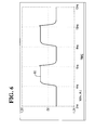
- FIG. 6 shows a PAM encoded signal output as used in the present invention.
- the output 60 is an encoded 1 Gb/sec signal in a 10011001 pattern.
- a 1 Gb/s digital signal has a fundamental analog frequency of 500 MHz and a pulse width of 1 ns as shown in FIG. 5.
- the fundamental frequency will usually dictate the pulse amplitude of the signal when it is received at the end of the loose transmission line.
- a quaternary PAM encoded signal has a fundamental analog frequency of 250 MHz and a pulsewidth of 2 ns as shown in FIG. 6.
- a different bit pattern was chosen for FIG. 6 because it is difficult to correlate a PAM data signal to a digital waveform.
- the pattern (10011001) was chosen for output 60 to illustrate the bandwidth conversion ability with the PAM encoding method of the present invention.
- FIG. 7 shows a Fast Fourier Transform (FFT) of the digital signal of FIG. 5.
- Major spectral components 62, 64, 66, and 68 of the FFT 70 show that several components, e.g., components 64, 66, and 68, are above the 1.5 GHz frequency level, and components 66 and 68 are above the 2.5 GHz level. Further, the fundamental frequency, component 62 of the FFT 70, is at 500 MHz.
- FIG. 8 shows a Fast Fourier Transform (FFT) of the PAM signal of FIG. 6.
- Major spectral components 72, 74, 76, 78, 80, and 82 of the FFT 84 show that the majority of the spectral components, e.g., components 72, 74, and 76, are below the 1.5 GHz frequency level, in sharp contrast to the FFT 70 of FIG. 7. Further, only component 82 is above the 2.5 GHz level, as opposed to components 66 and 68 of the FFT 70 of FIG. 7.
- the fundamental frequency, component 72 of FFT 84 is much lower in frequency than the fundamental frequency of FFT 70 shown in FIG. 7.
- This lowering of the fundamental frequency of the FFT 84 means that the PAM signal will have less attenuation and larger timing margins than a digital signal with the same amplitude. This allows the system designer to increase the data throughput of the system 10 system, because the designer has more bandwidth, without increasing the number of interconnects.
- the FFT 84 will vary for different data patterns due to the data-dependent frequencies of the signals, many of the FFT 84 components will still exist for almost all data patterns.
- the same data patterns as those used in FIGS. 5 and 6 were chosen.
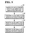
- FIG. 9 is a flowchart illustrating the steps used in the present invention.
- Block 86 represents the step of modulating a data stream with a pulse amplitude modulated encoder.
- Block 88 represents the step of transmitting the pulse amplitude modulated data stream on a transmission line.
- Block 90 represents the step of receiving the pulse amplitude modulated data stream at a receiver coupled to the transmission line.
- Block 92 represents the step of decoding the pulse amplitude modulated data stream.
Landscapes
- Physics & Mathematics (AREA)
- Spectroscopy & Molecular Physics (AREA)
- Engineering & Computer Science (AREA)
- Computer Networks & Wireless Communication (AREA)
- Signal Processing (AREA)
- Dc Digital Transmission (AREA)
- Time-Division Multiplex Systems (AREA)
- Information Transfer Systems (AREA)
Applications Claiming Priority (2)
| Application Number | Priority Date | Filing Date | Title |
|---|---|---|---|
| US99132497A | 1997-12-16 | 1997-12-16 | |
| US991324 | 1997-12-16 |
Publications (2)
| Publication Number | Publication Date |
|---|---|
| EP0924907A2 true EP0924907A2 (de) | 1999-06-23 |
| EP0924907A3 EP0924907A3 (de) | 2002-04-17 |
Family
ID=25537106
Family Applications (1)
| Application Number | Title | Priority Date | Filing Date |
|---|---|---|---|
| EP98309082A Withdrawn EP0924907A3 (de) | 1997-12-16 | 1998-11-05 | Multiplexierte Übertragung unter Verwendung von Pulsamplitudenmodulation |
Country Status (2)
| Country | Link |
|---|---|
| EP (1) | EP0924907A3 (de) |
| JP (1) | JPH11317774A (de) |
Cited By (2)
| Publication number | Priority date | Publication date | Assignee | Title |
|---|---|---|---|---|
| WO2004007201A1 (de) | 2002-07-16 | 2004-01-22 | Ebe Hesterman | Digitaldruckmaschine |
| US8452189B2 (en) | 2011-01-19 | 2013-05-28 | Avago Technologies General Ip (Singapore) Pte. Ltd. | Source-multiplexed pulse amplitude modulation (PAM) optical data communication system and method |
Families Citing this family (2)
| Publication number | Priority date | Publication date | Assignee | Title |
|---|---|---|---|---|
| DE20122739U1 (de) * | 2000-01-06 | 2007-08-23 | Rambus Inc., Los Altos | Kommunikationsschnittstelle mit mehrstufiger niedriger Verzögerung |
| KR100897280B1 (ko) | 2007-09-04 | 2009-05-14 | 주식회사 하이닉스반도체 | 리시버 회로 |
-
1998
- 1998-11-05 EP EP98309082A patent/EP0924907A3/de not_active Withdrawn
- 1998-12-10 JP JP35183298A patent/JPH11317774A/ja active Pending
Non-Patent Citations (1)
| Title |
|---|
| LEE, E.A.; MESSERSCHMITT, D.G.: "Digital Communications" , KLUWER ACADEMIC PUBLISHERS , BOSTON XP002189205 * paragraph [6.1.2] - paragraph [6.1.3]; figure 6.1 * * |
Cited By (2)
| Publication number | Priority date | Publication date | Assignee | Title |
|---|---|---|---|---|
| WO2004007201A1 (de) | 2002-07-16 | 2004-01-22 | Ebe Hesterman | Digitaldruckmaschine |
| US8452189B2 (en) | 2011-01-19 | 2013-05-28 | Avago Technologies General Ip (Singapore) Pte. Ltd. | Source-multiplexed pulse amplitude modulation (PAM) optical data communication system and method |
Also Published As
| Publication number | Publication date |
|---|---|
| JPH11317774A (ja) | 1999-11-16 |
| EP0924907A3 (de) | 2002-04-17 |
Similar Documents
| Publication | Publication Date | Title |
|---|---|---|
| KR100875348B1 (ko) | 클럭신호 및 데이터신호 결합 | |
| US7346094B2 (en) | System and method for transmitting data and additional information simultaneously within a wire based communication system | |
| US6463092B1 (en) | System and method for sending and receiving data signals over a clock signal line | |
| US5200979A (en) | High speed telecommunication system using a novel line code | |
| KR102452390B1 (ko) | 동기식으로 스위칭된 다중 입력 복조 비교기 | |
| EP3646520B1 (de) | Frequenz-/phasenumtastung für rückkanal-serdes-kommunikation | |
| CN102710240A (zh) | 信号处理装置、方法、serdes 和处理器 | |
| EP0299639A2 (de) | Digitales Datenübertragungssystem | |
| US8054867B2 (en) | Apparatus for transmitting data and additional information simultaneously within a wire-based communication system | |
| EP0924907A2 (de) | Multiplexierte Übertragung unter Verwendung von Pulsamplitudenmodulation | |
| EP2260595B1 (de) | System und verfahren für passive optische netzwerke mit zweifacher geschwindigkeit | |
| KR20020081248A (ko) | 클럭신호선을 통해 데이터신호를 송수신하기 위한 시스템및 방법 | |
| US6806817B2 (en) | Means and method of data encoding and communication at rates above the channel bandwidth | |
| US6580538B1 (en) | Reduction of optical impairments in wavelength division multiplexed systems employing a wavelength bus architecture | |
| KR100863369B1 (ko) | 사이클 인코딩된 신호에 관한 수신기 | |
| JPH10164010A (ja) | 光符号分割多重伝送アクセス方式及び装置 | |
| KR20210087859A (ko) | 다중 레벨 브레이드 신호법을 이용한 송수신 장치 및 그 동작 방법 | |
| JP2010288122A (ja) | 高速シリアル信号の伝送方法および変調、復調器 | |
| Popescu et al. | Experimental monolithic high speed transceiver for Manchester encoded data | |
| GB2318033A (en) | Transmission of a binary data flow | |
| Farzan et al. | A low-complexity power-efficient signaling scheme for chip-to-chip communication | |
| WO2002076052A2 (en) | Symmetric line coding | |
| CA2365608A1 (en) | System and method for high-speed skew-insensitive multi-channel data transmission | |
| WO2016144941A1 (en) | Clock and data recovery circuit for detection of multi-level input signals | |
| HK1083677B (en) | System and apparatus for encoding using different waveforms |
Legal Events
| Date | Code | Title | Description |
|---|---|---|---|
| PUAI | Public reference made under article 153(3) epc to a published international application that has entered the european phase |
Free format text: ORIGINAL CODE: 0009012 |
|
| AK | Designated contracting states |
Kind code of ref document: A2 Designated state(s): AT BE CH CY DE DK ES FI FR GB GR IE IT LI LU MC NL PT SE Kind code of ref document: A2 Designated state(s): DE FR GB |
|
| AX | Request for extension of the european patent |
Free format text: AL;LT;LV;MK;RO;SI |
|
| PUAL | Search report despatched |
Free format text: ORIGINAL CODE: 0009013 |
|
| AK | Designated contracting states |
Kind code of ref document: A3 Designated state(s): AT BE CH CY DE DK ES FI FR GB GR IE IT LI LU MC NL PT SE |
|
| AX | Request for extension of the european patent |
Free format text: AL;LT;LV;MK;RO;SI |
|
| 17P | Request for examination filed |
Effective date: 20021017 |
|
| AKX | Designation fees paid |
Free format text: DE FR GB |
|
| 17Q | First examination report despatched |
Effective date: 20021220 |
|
| STAA | Information on the status of an ep patent application or granted ep patent |
Free format text: STATUS: THE APPLICATION IS DEEMED TO BE WITHDRAWN |
|
| 18D | Application deemed to be withdrawn |
Effective date: 20031014 |