EP0924714B1 - Nonlinear resistor and manufacturing method of the same - Google Patents
Nonlinear resistor and manufacturing method of the same Download PDFInfo
- Publication number
- EP0924714B1 EP0924714B1 EP98124294A EP98124294A EP0924714B1 EP 0924714 B1 EP0924714 B1 EP 0924714B1 EP 98124294 A EP98124294 A EP 98124294A EP 98124294 A EP98124294 A EP 98124294A EP 0924714 B1 EP0924714 B1 EP 0924714B1
- Authority
- EP
- European Patent Office
- Prior art keywords
- nonlinear resistor
- electrodes
- electrode
- discharge energy
- sintered body
- Prior art date
- Legal status (The legal status is an assumption and is not a legal conclusion. Google has not performed a legal analysis and makes no representation as to the accuracy of the status listed.)
- Expired - Lifetime
Links
Images


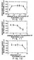

Classifications
-
- H—ELECTRICITY
- H01—ELECTRIC ELEMENTS
- H01C—RESISTORS
- H01C10/00—Adjustable resistors
- H01C10/04—Adjustable resistors with specified mathematical relationship between movement of resistor actuating means and value of resistance, other than direct proportional relationship
-
- H—ELECTRICITY
- H01—ELECTRIC ELEMENTS
- H01C—RESISTORS
- H01C7/00—Non-adjustable resistors formed as one or more layers or coatings; Non-adjustable resistors made from powdered conducting material or powdered semi-conducting material with or without insulating material
- H01C7/10—Non-adjustable resistors formed as one or more layers or coatings; Non-adjustable resistors made from powdered conducting material or powdered semi-conducting material with or without insulating material voltage responsive, i.e. varistors
- H01C7/105—Varistor cores
- H01C7/108—Metal oxide
- H01C7/112—ZnO type
-
- H—ELECTRICITY
- H01—ELECTRIC ELEMENTS
- H01C—RESISTORS
- H01C1/00—Details
- H01C1/14—Terminals or tapping points specially adapted for resistors; Arrangements of terminals or tapping points on resistors
- H01C1/142—Terminals or tapping points specially adapted for resistors; Arrangements of terminals or tapping points on resistors the terminals or tapping points being coated on the resistive element
-
- H—ELECTRICITY
- H01—ELECTRIC ELEMENTS
- H01C—RESISTORS
- H01C17/00—Apparatus or processes specially adapted for manufacturing resistors
- H01C17/28—Apparatus or processes specially adapted for manufacturing resistors adapted for applying terminals
Definitions
- the present invention relates to a nonlinear resistor employed in an arrester, a surge absorber, etc., i.e., a nonlinear resistor which includes zinc oxide as a main component and has a nonlinear resistance characteristic, and a method of manufacturing the nonlinear resistor.
- an overvoltage protection instrument such as an arrester, a surge absorber, etc. has been employed in the power system, and a nonlinear resistor has been frequently employed in such overvoltage protection instrument.
- the "nonlinear resistor” has a nonlinear resistance characteristic which exhibits an insulating characteristic at the normal voltage but exhibits a low resistance value when an overvoltage is applied to the nonlinear resistor.
- the overvoltage being superposed on the normal voltage can be removed by such nonlinear resistor. Therefore, the nonlinear resistor is extremely effective for the protection of the power system and the electrical machinery and apparatus.
- Such nonlinear resistor has a sintered body.
- the sintered body includes zinc oxide as a main component.
- the zinc oxide is mixed, granulated, formed, and sintered while adding at least one type metal oxide as an additive to achieve the nonlinear resistance characteristic.
- Insulating layers are also formed on side surfaces of each sintered body, and electrodes formed of aluminum, etc. are formed on an upper surface and a lower surface of the sintered body by an arc thermal spraying, etc.
- Discharge energy withstand is set to the above-mentioned nonlinear resistor. Then, the nonlinear resistor is brought into breakdown mechanically or electrically if the discharge energy being applied to the nonlinear resistor exceeds this discharge energy withstand. As one of breakdown types of the nonlinear resistor caused when such nonlinear resistor absorbs the discharge energy, there is breakdown which is due to an electrode layer of the nonlinear resistor. More particularly, the nonlinear resistor comes to breakdown in following cases. That is, there are cases where,
- JP-A-02 058807 describes a nonlinear resistor and a method for fabricating it.
- Said nonlinear resistor comprises a sintered body composed principally of zinc oxide and has an upper, lower and side surface. An insulating layer is formed on the side surface.
- the nonlinear resistor furthermore comprises electrodes formed on the upper and lower surfaces by spraying.
- the present invention has been made to overcome the problems as described above in the related art, and it is an object of the present invention to provide a nonlinear resistor which is able to prevent its breakdown due to an electrode of the nonlinear resistor in receiving a discharge energy by restricting electrode forming conditions and material or shape of the electrode, to have an extremely excellent discharge energy withstand characteristic.
- a nonlinear resistor which is defined by the features of claim 1. It comprises a sintered body including a zinc oxide as a main component, said sintered body having an upper surface, a lower surface, and a side surface; a insulating layer formed on the side surface of the sintered body; and a pair of electrodes formed on the upper surface and the lower surface of the sintered body respectively by a plasma thermal spraying.
- nonlinear resistor of the present invention constructed as above, unevenness of the current distribution in the sintered body while absorbing the discharge energy can be prevented by optimizing the conditions of the plasma thermal spraying to form the electrodes, so that the high discharge energy withstand can be achieved.
- the electrode is formed by the plasma thermal spraying in an atmosphere in which an oxygen concentration is set to less than or equal to 22 volume %.
- the electrode is formed by the plasma thermal spraying of which an output is set to less than or equal to 10 kW.
- the electrode is formed by the plasma thermal spraying of low output such as 10 kW or less, the electrode of a predetermined shape can be easily obtained.
- residual stress of the thermal spraying electrode film can be suppressed, an adhesion force between the electrode and the sintered body can be enhanced to prevent peel between them, and the high discharge energy withstand can be attained.
- the electrode is formed of any one of aluminum, copper, zinc, nickel, and silver or their alloy.
- any one of aluminum, copper, zinc, nickel, and silver or their alloy is employed as material of the electrode, the conductivity of the electrode and the adhesion force between the electrode and the sintered body can be enhanced, so that the excellent discharge energy withstand can be achieved.
- the electrode is formed by a metal powder, and an average particle size of the metal powder is set in a range of 5 ⁇ m to 50 ⁇ m.
- powder evaporation in plasma thermal spraying can be prevented by setting the average particle size of the metal powders of the electrodes to more than or equal to 5 ⁇ m. Therefore, unevenness of the current distribution in the sintered body due to lack in film thickness caused by the evaporation can be prevented.
- an amount of unmelted particles during the plasma thermal spraying can be reduced by setting the average particle size of the metal powders of the electrodes to less than or equal to 50 ⁇ m. Accordingly, the voids in the electrode can be reduced by suppressing an amount of unmelted particles stuck onto the sintered body, so that the high discharge energy withstand can be achieved.
- the upper surface and the lower surface of the sintered body have an average surface roughness within a range of 3 ⁇ m to 8 ⁇ m.
- the average surface roughness of the surface of the sintered body in forming the electrode is set larger than or equal to 3 ⁇ m, the surface area of the sintered body to sufficiently ensure the adhesion force between the sintered body and the electrode can be obtained.
- the average surface roughness of the surface of the sintered body in forming the electrode is suppressed smaller than or equal to 8 ⁇ m, unevenness of the current distribution at the convex top end of the sintered body can be prevented. Accordingly, the discharge energy withstand of the nonlinear resistor can be enhanced.
- the electrode has a porosity of less than or equal to 15 %.
- nonlinear resistor having the above structure, since the porosity of the electrodes is set to less than or equal to 15 %, generation of the discharge in the voids can be prevented by reducing the voids in the electrode, and at the same time unevenness of the current distribution due to clearances on the interface between the sintered body and the electrode can be prevented. Accordingly, the discharge energy withstand of the nonlinear resistor can be enhanced.
- the electrode contains a metal oxide and a metal, and a weight percentage of the metal oxide contained in the electrode is set to less than or equal to 25 %.
- the electrode has an average thickness in a range of 5 ⁇ m to 500 ⁇ m.
- the average thickness of the electrode is set in the range of 5 ⁇ m to 500 ⁇ m, lack in film thickness and adhesion defect of the electrode can be prevented, and also peel of the sintered body and the electrode because of increase in residual stress in the electrodes can be prevented. Accordingly, unevenness of the current distribution in the sintered body due to such lack in film thickness, adhesion defect, peel, etc. can be prevented, so that the high discharge energy withstand of the nonlinear resistor can be attained.
- the electrode has an average surface roughness of less than or equal to 8 ⁇ m.
- the electrode has a resistivity of less than or equal to 15 ⁇ ⁇ cm.
- nonlinear resistor having the above structure, since the resistivity of the electrode is set to less than or equal to 15 ⁇ cm, no high resistance area is formed on the interface between the sintered body and the electrode. Accordingly, unevenness of the current distribution in the nonlinear resistor can be prevented, so that the high discharge energy withstand of the nonlinear resistor can be attained.
- the electrode has a side end portion and the sintered body has a side end portion, and a distance between the side end portion of the electrode and the side end portion of the sintered body is set in a range of 0.01 mm to 1.0 mm.
- nonlinear resistor having the above structure, since the distance between the side end portion of the electrode and the side end portion of the sintered body is limited from 0.01 mm to 1.0 mm, i.e., electrode forming range is limited, generation of the discharge between the electrodes as well as unevenness of the current distribution in the nonlinear resistor can be prevented. Accordingly, local unevenness of the current distribution in the sintered body while absorbing the discharge energy can be prevented, so that the high discharge energy withstand of the nonlinear resistor can be attained.
- the electrode has a side end portion which has an unevenness in a direction parallel with the upper surface or the lower surface of the sintered body, a variation of the unevenness is set in a range of ⁇ 0.5 mm.
- a method of manufacturing the nonlinear resistor comprises the steps of: (a) forming a sintered body by sintering a material including a zinc oxide as a main component, said sintered body having an upper surface, a lower surface, and a side surface; (b) forming an insulating layer on the side surface of the sintered body; and (c) forming a pair of electrodes on the upper surface and the lower surface of the sintered body respectively by a plasma spraying.
- the plasma spraying is performed in an atmosphere in which an oxygen concentration is set to less than or equal to 22 volume %.
- an output of the plasma spraying is set to less than or equal to 10kW.
- the electrode is formed of any one of aluminum, copper, zinc, nickel, and silver or their alloy.
- the electrode is formed by a metal powder, and an average particle size of the metal powder is set in a range of 5 ⁇ m to 50 ⁇ m.
- the upper surface and the lower surface of the sintered body have an average surface roughness within a range of 3 ⁇ m to 8 ⁇ m.
- the electrode has a porosity of less than or equal to 15 %.
- the electrode contains a metal oxide and a metal, and a weight percentage of the metal oxide contained in the electrode is set to less than or equal to 25 %.
- the electrode has an average thickness in a range of 5 ⁇ m to 500 ⁇ m.
- the electrode has an average surface roughness of less than or equal to 8 ⁇ m.
- the electrode has a resistivity of less than or equal to 15 ⁇ cm.
- the electrode has a side end portion and the sintered body has a side end portion, and a distance between the side end portion of the electrode and the side end portion of the sintered body is set in a range of 0.01 mm to 1.0 mm.
- the electrode has a side end portion which has an unevenness in a direction parallel with the upper surface or the lower surface of the sintered body, a variation of the unevenness is set in a range of ⁇ 0.5 mm.
- a nonlinear resistor according to a first embodiment of the present invention will be explained with reference to FIGS.1 to 3 hereinbelow.
- FIG. 1 is a sectional view showing the nonlinear resistor according to the first embodiment.
- this nonlinear resistor has a sintered body 1 which is formed to include zinc oxide as a main component.
- This sintered body 1 has an upper surface 1a, a lower surface 1b, and a side surface 1c.
- An insulating layer is formed on the side surface 1c of the sintered body 1, and a pair of electrodes 3 are formed on the upper surface 1a and the lower surface 1b of the sintered body 1.
- the electrodes 3 are formed by plasma thermal spraying.
- This plasma thermal spraying is carried out in an atmosphere in which an oxygen concentration is set to less than or equal to 22 volume %.
- material of the nonlinear resistor is prepared by adding manganese dioxide (MnO2), cobalt oxide (Co2O3), bismuth oxide (Bi2O3), antimony oxide (Sb2O3), and nickel oxide (NiO) as metal oxides to zinc oxide (ZnO) as a main component.
- MnO2 manganese dioxide
- Co2O3 cobalt oxide
- Bi2O3 bismuth oxide
- Sb2O3 antimony oxide
- NiO nickel oxide
- ZnO zinc oxide
- alumina group inorganic insulator is coated on the side surface 1c of the sintered body 1, and then side surface insulating film 2 is formed on the side surface 1c by baking the inorganic insulator at 400 °C. Then, main upper and lower surfaces 1a, 1b of the sintered body 1 which has the side surface insulating film 2, are polished respectively, and then a guard mask is covered on the sintered body 1. Then, the electrodes 3 are formed on polished upper and lower surfaces by the plasma thermal spraying. As above, the nonlinear resistor can be fabricated.
- a sample is prepared by stacking three sheets of nonlinear resistors which are fabricated under the same conditions. Then, while increasing a discharge energy amount from 200 J/cc by 20 J/cc, rectangular discharge energy of 2 ms has been applied to respective samples at a five minute interval. Thus, a destructive test is conducted until at least one sheet of three nonlinear resistors is destroyed electrically. At this time, a maximum value of the discharge energy amount being absorbed to cause the destroy of the sample is assumed as discharge energy withstand (J/cc). As with respective electrode forming conditions or electrode shape of the nonlinear resistor, the discharge energy withstand test is applied to ten sets of nonlinear resistors.
- FIG.2 is a graph showing the result of the discharge energy withstand test of the nonlinear resistor according to the first embodiment when the thermal spraying method of forming the electrode of the nonlinear resistor is changed.
- a reference 4 denotes a nonlinear resistor having electrodes which are formed by the non- vacuum arc thermal spraying; 5, nonlinear resistor having electrodes which are formed by the non-vacuum high-speed gas flame thermal spraying; and 6, nonlinear resistor having electrodes which are formed by the non-vacuum plasma thermal spraying.
- the discharge energy withstand of the nonlinear resistor is clearly enhanced rather than the case where the electrodes 3 of the nonlinear resistor 4 is formed by the non-vacuum arc thermal spraying or the case where the electrodes 3 of the nonlinear resistor 5 is formed by the non-vacuum high-speed gas flame thermal spraying.
- the electrodes are formed by the arc thermal spraying, thermal spraying particles being melted and sprayed onto the electrodes are large, and thus a surface of the electrode is not smooth and a number of pores and oxides are contained in the electrode. Hence, the nonlinear resistor having excellent discharge energy withstand has not been able to be implemented.
- the electrodes are formed by the high-speed gas flame thermal spraying, a spraying pressure in spraying is high, and thus a guard mask of the electrodes is easily deformed in spraying. Hence, the electrode cannot be formed into a predetermined shape. As a result, the nonlinear resistor having excellent discharge energy withstand has not been available.
- the nonlinear resistor according to the first embodiment in which the electrodes 3 are formed by the plasma thermal spraying, exhibits a remarkably excellent discharge energy withstand characteristic. This is because the electrode 3 being formed by the plasma thermal spraying has a smooth surface, and the pores and the oxides are less contained in the electrodes 3, and the electrode 3 can be formed to have a predetermined shape. The nonlinear resistor having such electrodes 3 can have the excellent discharge energy withstand.
- FIG.3 is a graph showing the result of the discharge energy withstand test of the nonlinear resistor whose electrodes 3 are formed by using the plasma thermal spraying, while changing an oxygen concentration in a thermal spraying atmosphere, when the electrodes 3 of the nonlinear resistor according to the first embodiment of the present invention is formed.
- the nonlinear resistor shows the remarkably excellent discharge energy withstand since an amount of oxide in the thermal spraying electrode is small.
- the electrodes 3 of the nonlinear resistor is formed by using the plasma thermal spraying in the atmosphere which contains the oxygen concentration of less than or equal to 22 volume %
- planalization of the surface of the electrodes 3 can be advanced by suppressing an amount of oxide in the thermal spraying electrode smaller to thus reduce voids in the electrodes 3. For this reason, unevenness of current distribution in the sintered body 1 while absorbing the discharge energy can be prevented and thus the nonlinear resistor can have excellent discharge energy withstand.
- nonlinear resistors are fabricated.
- Such nonlinear resistors have the electrodes 3 which are formed under different electrode forming conditions, but satisfying at least the condition for the electrodes 3 in the first embodiment, i.e., "the electrodes 3 are formed by the plasma thermal spraying in the atmosphere in which the oxygen concentration is set to less than or equal to 22 volume %" in the nonlinear resistor manufacturing steps set forth in the first embodiment.
- the nonlinear resistors are fabricated under plural electrode forming conditions such as (2-1) thermal spraying output, (2-2) material of electrode, (2-3) average particle size of thermal spraying powder employed in forming the electrodes, and (2-4) surface roughness of a sintered body 1 on which the electrodes are formed. Then, while changing each objective condition as a parameter, the discharge energy withstand test is applied to several types of the nonlinear resistors respectively under the same discharge energy withstand test conditions as the above first embodiment.
- Plural electrode forming conditions being set actually to respective withstand conditions, and results of the discharge energy withstand test of several types of the nonlinear resistors which have the electrodes 3 formed under the plural electrode forming conditions will be explained separately in the following.
- FIG.4 is a graph showing a relationship between the thermal spraying output (kW) and the discharge energy withstand (J/cc).
- the nonlinear resistor whose electrodes 3 are formed at the thermal spraying output below or equal to 10 kW shows on an average the high discharge energy withstand in excess of 500 J/cc, whereas the nonlinear resistor whose electrodes 3 are formed at the thermal spraying output of more than 10 kW shows the low discharge energy withstand.
- the thermal spraying output is high and thus the electrode 3 having the predetermined shape is difficult to be formed.
- the thermal spraying speed is high at the high output in excess of 10 kW, residual stress of the thermal spraying electrode film becomes high.
- the electrodes 3 having the predetermined shape can be easily formed and residual stress of the thermal spraying electrode film becomes low.
- the thermal-sprayed electrode having high adhesiveness can be formed and also the nonlinear resistor can have the excellent discharge energy withstand.
- FIG.5 is a graph showing a relationship between material of the electrode 3 of the nonlinear resistor according to the second embodiment and the discharge energy withstand (J/cc). More specifically, FIG.5 shows results of the discharge energy withstand test of the nonlinear resistor in which powder material is varied when the electrodes 3 of the nonlinear resistor are formed by using the plasma thermal spraying. FIG.5 shows the discharge energy withstand of the nonlinear resistors which employ material such as aluminum 7, copper 8, zinc 9, nickel 10, silver 11, alloy of copper and zinc 12, alloy of nickel and aluminum 13, alloy of silver and copper 14, carbon steel 15, and 13 % Cr stainless steel 16, as the material of the electrodes 3, respectively.
- the nonlinear resistors in which the material of the electrodes 3 is formed of aluminum 7, copper 8, zinc 9, nickel 10, silver 11, alloy of copper and zinc 12, alloy of nickel and aluminum 13, or alloy of silver and copper 14 show on an average the excellent discharge energy withstand in excess of 500 J/cc, nevertheless the discharge energy withstand is low in the nonlinear resistors in which the material of the electrodes 3 is formed of carbon steel 15 or 13 % Cr stainless steel 16.
- the nonlinear resistor in which the electrodes 3 are formed by using the carbon steel 15 or the 13 % Cr stainless steel 16 as the material of the electrode 3 a conductivity of the electrode 3 is low and also adhesiveness between the sintered body 1 and the electrodes 3 is small.
- the discharge energy withstand of the nonlinear resistor becomes low.
- the conductivity and adhesiveness to the sintered body 1 can be enhanced in the electrodes 3 using aluminum, copper, zinc, nickel, silver, or their alloy as the material of the electrodes 3. For this reason, the nonlinear resistor having such electrodes 3 can get the excellent discharge energy withstand.
- FIG.6 is a graph showing a relationship between an average particle size ( ⁇ m) of metal powders and the discharge energy withstand (J/cc) when the electrodes 3 of the nonlinear resistor are formed. More specifically, FIG.6 shows results of the discharge energy withstand test of the nonlinear resistor in which the electrodes 3 are formed by changing the particle size of aluminum material in the plasma thermal spraying. In this case, the average particle size of the metal powders is a 50 % particle size derived by the laser diffraction method.
- the nonlinear resistor whose electrodes 3 are formed by using the metal powders an average particle size of which is ranging from 5 ⁇ m to 50 ⁇ m in the thermal spraying electrode, shows on an average the high discharge energy withstand in excess of 500 J/cc.
- the discharge energy withstand is reduced.
- the average particle size of the metal powders is smaller than 5 ⁇ m in forming the electrodes 3, the particle size of the metal powders in the nonlinear resistor being fabricated by using the metal powders is too small. Consequently, a great deal of powders are evaporated in plasma thermal spraying, so that areas in which the electrodes 3 are not formed on the thermal spraying electrode layers are partially produced. Accordingly, both the areas in which the electrodes 3 are formed and the areas in which the electrodes 3 are not formed are present together, so that the current distribution in the sintered body 1 as the nonlinear resistor becomes uneven. As a result, the discharge energy withstand is decreased.
- the average particle size of the metal powders exceeds 50 ⁇ m in forming the electrodes 3, the particle size of the metal powders is too large in the nonlinear resistor being fabricated by using the metal powders.
- an amount of metal powders which are stuck onto the sintered body 1 as the nonlinear resistor as unmelted particles yet in the plasma thermal spraying is enhanced. For this reason, the number of voids is increased in the thermal spraying electrode, so that the discharge energy withstand is lowered.
- the nonlinear resistor having the electrodes 3 in which the average particle size of the metal powders is limited in the range of 5 ⁇ m to 50 ⁇ m unevenness of the current distribution in the sintered body 1 due to lack in film thickness caused by evaporation can be prevented by preventing the evaporation of the metal powders in plasma thermal spraying, and at the same time the voids in the electrodes 3 can be reduced by reducing an amount of unmelted particles during the plasma thermal spraying and suppressing an amount of unmelted particles stuck onto the sintered body 1. Therefore, the above nonlinear resistor can achieve the high discharge energy withstand.
- FIG.7 is a graph showing a relationship between average surface roughness ( ⁇ m) of the sintered body 1 and the discharge energy withstand (J/cc) when the electrodes 3 of the nonlinear resistor according to the second embodiment of the present invention is formed. More specifically, the electrodes 3 are formed after both end surfaces of the sintered body 1 have been polished when the nonlinear resistor is fabricated.
- FIG.7 shows the results of the discharge energy withstand test of the nonlinear resistor in which the electrodes 3 are formed by changing the surface roughness of the sintered body 1, e.g., by changing the grain size of the polishing grinder, applying the blast process to the sintered body 1 by changing the grain size of the abrasive grains after the polishing, or the like.
- the nonlinear resistor in which the surface roughness of the sintered body 1 constituting the electrodes 3 of the nonlinear resistor is set in the range of 3 ⁇ m to 8 ⁇ m, exhibits on an average the high discharge energy withstand in excess of 500 J/cc.
- the discharge energy withstand becomes small.
- the nonlinear resistor being fabricated to reduce the average surface roughness of the sintered body 1 smaller than 3 ⁇ m in forming the electrodes 3 has a small surface area of the sintered body 1, adhesion strength between the sintered body 1 and the electrodes 3 is small and thus peel of the electrodes 3 is easily caused at end portions of the electrodes 3. Therefore, the discharge energy withstand becomes small.
- the nonlinear resistor which is fabricated by setting the average surface roughness of the sintered body 1 larger than 8 ⁇ m in forming the electrodes 3, when the discharge energy is absorbed by the nonlinear resistor, the current distribution becomes uneven at the concave top ends on the surface of the sintered body 1. As a result, the discharge energy withstand is reduced.
- the nonlinear resistor in which the average surface roughness of the sintered body 1 is set in the range of 3 ⁇ m to 8 ⁇ m, a strong adhesion force between the sintered body 1 and the electrodes 3 can be assured. At the same time, unevenness of the current distribution at the concave top ends on the surface of the sintered body 1 can be prevented and thus the nonlinear resistor can have the excellent discharge energy withstand.
- the electrodes 3 are formed by using the plasma thermal spraying having the output of 10 kW or below and also any one of aluminum, copper, zinc, nickel, and silver or their alloy is employed as material of the electrodes 3.
- the average particle size of the metal powders as the material of the electrodes 3 is set in the range of 5 ⁇ m to 50 ⁇ m, and the upper surface 1a and the lower surface 1b of the sintered body 1 are set to have the average surface roughness in the range of 3 ⁇ m to 8 ⁇ m.
- FIGS.8 to 12 a third embodiment of the present invention will be explained with reference to FIGS.8 to 12 hereunder.
- the nonlinear resistors have the electrodes 3 which have different characteristics by changing electrode forming conditions variously, but satisfying at least the condition for the electrodes 3 in the first embodiment, i.e., "the electrodes 3 are formed by the plasma thermal spraying in the atmosphere in which the oxygen concentration is set to less than or equal to 22 volume %" in the nonlinear resistor manufacturing steps set forth in the first embodiment.
- the nonlinear resistors are fabricated under plural electrode forming conditions such as (3-1) porosity, (3-2) weight percentage of metal oxide, (3-3) average film thickness, (3-4) average surface roughness, and (3-5) resistivity. Then, while changing each objective condition as a parameter, the discharge energy withstand test is applied to several types of the nonlinear resistors respectively under the same discharge energy withstand test conditions as the above first embodiment.
- Plural electrode forming conditions being set actually to respective withstand conditions, and results of the discharge energy withstand test of several types of the nonlinear resistors which have the electrodes 3 formed under the plural electrode forming conditions will be explained separately in the following.
- FIG.8 is a graph showing a relationship between a porosity (%) of the electrode of the nonlinear resistor according to a third embodiment of the present invention and the discharge energy withstand (J/cc). More specifically, FIG.8 shows results of the discharge energy withstand test of the nonlinear resistors in which porosity in the thermal spraying electrode is varied by changing the conditions when the electrodes 3 are formed by the thermal spraying. In this case, after a test piece made of only the thermal spraying electrode has been picked up from the nonlinear resistor, the porosity is measured by executing a mercury injection test of the test piece.
- the nonlinear resistor in which the porosity of the electrodes 3 is less than or equal to 15 % shows on an average the high discharge energy withstand of more than 500 J/cc, while the discharge energy withstand is low in the nonlinear resistor in which the porosity of the electrodes 3 exceeds 15 %.
- the current distribution in the nonlinear resistor is made uneven by the pores on the interface between the sintered body 1 and the electrodes 3 of the nonlinear resistor when the nonlinear resistor absorbs the discharge energy, so that the discharge energy withstand is degraded.
- the nonlinear resistor having the excellent discharge energy withstand can be provided by suppressing the porosity of the electrodes 3 in the nonlinear resistor below or equal to 15 %.
- FIG.9 is a graph showing a relationship between a weight percentage (%) of metal oxide in the electrode 3 of the nonlinear resistor according to the third embodiment of the present invention and the discharge energy withstand (J/cc). More specifically, FIG.9 shows results of the discharge energy withstand test of the nonlinear resistors in which the weight percentage of the metal oxide in the thermal spraying electrode is varied by changing the conditions when the electrodes 3 are formed by the thermal spraying. In this case, after a test piece made of only the thermal spraying electrode has been picked up from the nonlinear resistor, the weight percentage of the metal oxide is calculated by detecting an amount of oxygen in the test piece by using a burning method.
- the nonlinear resistor in which the metal oxide in the electrodes 3 is less than or equal to 25 wt% shows on an average the high discharge energy withstand of more than 500 J/cc, while the discharge energy withstand is low in the nonlinear resistor in which the metal oxide in the electrodes 3 exceeds 25 wt%.
- the current distribution in the nonlinear resistor is made uneven by the presence of the metal oxide on the interface between the sintered body 1 and the electrodes 3 of the nonlinear resistor when the nonlinear resistor absorbs the discharge energy, so that the discharge energy withstand is degraded.
- the metal oxide in the electrodes 3 is less than or equal to 25 wt%, unevenness of the current distribution in the nonlinear resistor due to the metal oxide on the interface between the sintered body 1 and the electrodes 3 of the nonlinear resistor can be prevented. Therefore, the excellent discharge energy withstand of the nonlinear resistor can be achieved. In this manner, the nonlinear resistor having the excellent discharge energy withstand can be provided by suppressing the metal oxide in the electrodes 3 in the nonlinear resistor below or equal to 25 wt%.
- FIG.10 is a graph showing a relationship between an average film thickness ( ⁇ m) of the electrode of the nonlinear resistor according to the third embodiment of the present invention and the discharge energy withstand (J/cc). More specifically, FIG.10 shows results of the discharge energy withstand test of the nonlinear resistors in which the average film thickness of the thermal spraying electrode is varied by changing the conditions when the electrodes 3 are formed by the thermal spraying.
- the average film thickness of the electrode is a mean film thickness which is detected from a film thickness in a microscopic photograph showing a sectional shape of the electrode 3.
- the nonlinear resistor in which the average film thickness of the electrode 3 is set in the range of 5 ⁇ m to 500 ⁇ m shows on an average the high discharge energy withstand of more than 500 J/cc, but the discharge energy withstand is low in the nonlinear resistor in which the average film thickness of the electrodes 3 is thinner than 5 ⁇ m or the average film thickness of the electrodes 3 is thicker than 500 ⁇ m.
- the current distribution in the sintered body 1 of the nonlinear resistor becomes uneven in such peeled area when the nonlinear resistor absorbs the discharge energy, so that the discharge energy withstand is also degraded.
- the average film thickness of the electrodes 3 is set in the range of 5 ⁇ m to 500 ⁇ m, film thickness insufficiency and adhesion defect in the electrodes 3 of the nonlinear resistor can be prevented and also the peel caused between the sintered body 1 and the electrodes 3 by the increase in residual stress in the electrodes 3 can be prevented. Therefore, unevenness of the current distribution in the nonlinear resistor due to the above can be prevented, and the excellent discharge energy withstand of the nonlinear resistor can be achieved. As described above, according to the nonlinear resistor in which the average film thickness of the electrodes 3 is set in the range of 5 ⁇ m to 500 ⁇ m, the excellent discharge energy withstand can be provided.
- FIG.11 is a graph showing a relationship between average surface roughness ( ⁇ m) of the electrode of the nonlinear resistor according to the third embodiment of the present invention and the discharge energy withstand (J/cc). More specifically, FIG. 11 shows results of the discharge energy withstand test of the nonlinear resistors in which the average surface roughness of the thermal spraying electrode is varied by changing the conditions when the electrodes 3 are formed by the thermal spraying.
- the nonlinear resistor in which the average surface roughness of the electrodes 3 is less than or equal to 8 ⁇ m shows on an average the high discharge energy withstand of more than 500 J/cc, but the discharge energy withstand is reduced in the nonlinear resistor in which the average surface roughness of the electrodes 3 exceeds 8 ⁇ m.
- the discharge energy withstand is reduced in the nonlinear resistor in which the average surface roughness of the electrodes 3 exceeds 8 ⁇ m.
- the excellent discharge energy withstand of the nonlinear resistor can be achieved because the discharge caused in the clearances between the stacked nonlinear resistors can be prevented. That is to say, the nonlinear resistor having the excellent discharge energy withstand can be provided by suppressing the average surface roughness of the electrodes 3 in the nonlinear resistor below or equal to 8 ⁇ m.
- FIG.12 is a graph showing a relationship between a resistivity ( ⁇ cm) of the electrode of the nonlinear resistor according to the third embodiment of the present invention and the discharge energy withstand (J/cc). More specifically, FIG.12 shows results of the discharge energy withstand test of the nonlinear resistors in which the resistivity of the thermal spraying electrode is varied by changing the conditions when the electrodes 3 are formed by the thermal spraying. In this case, after a test piece made of only the thermal spraying electrode has been picked up from the nonlinear resistor, a resistance value of the test piece is detected by a DC four terminal method and then the resistivity is calculated based on the resistance value and a shape of the test piece.
- the nonlinear resistor in which the resistivity of the electrodes 3 is less than or equal to 15 ⁇ cm shows on an average the high discharge energy withstand of more than 500 J/cc, whereas the discharge energy withstand becomes low in the nonlinear resistor in which the resistivity of the electrodes 3 exceeds 15 ⁇ cm.
- the resistivity of the electrodes 3 is less than or equal to 15 ⁇ cm, unevenness of the current distribution in the nonlinear resistor due to the high resistance areas formed on the interface between the sintered body 1 and the electrodes 3 of the nonlinear resistor can be prevented. Therefore, the excellent discharge energy withstand of the nonlinear resistor can be achieved.
- the nonlinear resistor having the excellent discharge energy withstand can be provided by suppressing the resistivity of the electrodes 3 in the nonlinear resistor below or equal to 15 ⁇ cm.
- the porosity of the electrodes 3 is set to less than or equal to 15 % and also the weight percentage of the metal oxide in the electrodes 3 is set to less than or equal to 25 %. Furthermore, the average film thickness of the electrodes 3 is set in the range of 5 ⁇ m to 500 ⁇ m, the average surface roughness is set to less than or equal to 8 ⁇ m, and the resistivity is set to less than or equal to 15 ⁇ cm.
- a fourth embodiment of the present invention will be explained with reference to FIGS.13 to 15 hereunder.
- the nonlinear resistors have the electrodes 3 which have different shapes by changing electrode forming conditions variously, but satisfying at least the condition for the electrodes 3 in the first embodiment, i.e., "the electrodes 3 are formed by the plasma thermal spraying in the atmosphere in which the oxygen concentration is set to less than or equal to 22 volume %" in the nonlinear resistor manufacturing steps set forth in the first embodiment.
- the dimension of the electrodes 3 and uneven sizes at the end portions are changed variously by changing the method of forming the electrodes 3 and its conditions variously out of the above nonlinear resistor manufacturing steps, so that the nonlinear resistors having the electrodes 3 of different dimensions and shape can be fabricated.
- FIG.13 is a schematic view showing an electrode side end portion of the nonlinear resistor fabricated as above.
- a reference 17 denotes a sintered body side end portion; 18, an electrode; and 19, an electrode side end portion.
- a reference 21 denotes a distance between a parallel line 20 indicating an average position of the end portion along the diameter direction of the electrode 3 and the sintered body side end portion 17, i.e., an average distance between the electrode side end portion 19 and the sintered body side end portion 17.
- a reference 22 denotes a maximum value in variation of the unevenness of the electrode side end portion 19.
- the nonlinear resistors are fabricated under plural electrode forming conditions such as (4-1) a distance between an electrode side end portion and a sintered body side end portion, and (4-2) a maximum value of unevenness of the electrode side end portion along the main surface direction. Then, while changing each objective condition as a parameter, the discharge energy withstand test is applied to several types of the nonlinear resistors respectively under the same discharge energy withstand test conditions as the above first embodiment.
- Plural electrode forming conditions being set actually to respective withstand conditions, and results of the discharge energy withstand test of several types of the nonlinear resistors which have the electrodes 3 formed under the plural electrode forming conditions will be explained separately in the following.
- FIG.14 is a graph showing a relationship between a distance (mm) 21 between the electrode side end portion 19 and the sintered body side end portion 17 of the nonlinear resistor according to the fourth embodiment of the present invention and the discharge energy withstand (J/cc). More specifically, FIG.14 shows results of the discharge energy withstand test of the nonlinear resistors in which the shape of the thermal spraying electrode is varied by changing the conditions when the electrodes 3 are formed by the thermal spraying.
- the nonlinear resistor in which the distance 21 between the electrode side end portion 19 and the sintered body side end portion 17 is set in the range of 0.01 mm to 1.0 mm shows on an average the high discharge energy withstand of more than 500 J/cc, whereas the discharge energy withstand becomes low in the nonlinear resistor in which the distance 21 between the electrode side end portion 19 and the sintered body side end portion 17 is shorter than 0.01 mm or the distance 21 between the electrode side end portion 19 and the sintered body side end portion 17 is longer than 1.0 mm.
- the distance 21 between the electrode side end portion 19 and the sintered body side end portion 17 of the nonlinear resistor is shorter than 0.01 mm, dielectric breakdown is ready to occur on the interface between the sintered body 1 and a side surface insulating layer of the nonlinear resistor, or in the side surface insulating layer, or on the side surfaces of the side surface insulating layer when the nonlinear resistor absorbs the discharge energy. As a result, the discharge energy withstand of the nonlinear resistor is degraded.
- the discharge energy withstand of the nonlinear resistor is also degraded since the current distribution in the sintered body 1 of the nonlinear resistor becomes uneven when the nonlinear resistor absorbs the discharge energy.
- the distance 21 between the electrode side end portion 19 and the sintered body side end portion 17 of the nonlinear resistor is set in the range of 0.01 mm to 1.0 mm, the dielectric breakdown being caused on the interface between the sintered body 1 and the side surface insulating layer, or in the side surface insulating layer, or on the side surfaces of the side surface insulating layer when the nonlinear resistor absorbs the discharge energy, or unevenness of the current distribution in the nonlinear resistor can be prevented. Therefore, the excellent discharge energy withstand of the nonlinear resistor can be achieved.
- the nonlinear resistor having the excellent discharge energy withstand can be provided by setting the distance 21 between the electrode side end portion 19 and the sintered body side end portion 17 of the nonlinear resistor in the range of 0.01 mm to 1.0 mm.
- FIG.15 is a graph showing a relationship between a maximum value 22 ( ⁇ mm) of unevenness of the electrode side end portion 19 of the nonlinear resistor according to the fourth embodiment of the present invention and the discharge energy withstand (J/cc) of the nonlinear resistor. More specifically, FIG.15 shows results of the discharge energy withstand test of the nonlinear resistors in which the shape of the thermal spraying electrode is varied by changing the conditions when the electrodes 3 are formed by the thermal spraying.
- the nonlinear resistor in which the maximum value 22 of unevenness of the electrode side end portion 19 is set in a range of ⁇ 0.5 mm shows on an average the high discharge energy withstand of more than 500 J/cc, while the discharge energy withstand is low in the nonlinear resistor in which the maximum value 22 in variation of the unevenness of the electrode side end portion 19 is set outside of the range of ⁇ 0.5 mm.
- the current distribution in the sintered body 1 of the nonlinear resistor is made uneven at the convex top end of the electrode side end portion 19 of the nonlinear resistor when the nonlinear resistor absorbs the discharge energy, so that the discharge energy withstand of the nonlinear resistor is degraded.
- the maximum value 22 in variation of the unevenness of the electrode side end portion 19 of the nonlinear resistor is set in the range of ⁇ 0.5 mm, the excellent discharge energy withstand of the nonlinear resistor can be achieved since unevenness of the current distribution in the nonlinear resistor due to the convex top end of the electrode side end portion 19 can be prevented.
- the nonlinear resistor having the excellent discharge energy withstand can be provided by suppressing the maximum value 22 in variation of the unevenness of the electrode side end portion 19 of the nonlinear resistor within the range of ⁇ 0.5 mm.
- the distance 21 between the electrode side end portion 19 and the sintered body side end portion 17 of the nonlinear resistor is set in the range of 0.01 mm to 1.0 mm, and also the maximum value 22 in variation of the unevenness of the electrode side end portion 19 of the nonlinear resistor is set within the range of ⁇ 0.5 mm.
- the present invention unevenness of the current distribution caused in the sintered body in absorbing the discharge energy can be prevented by limiting the electrode forming conditions by using the plasma thermal spraying and the material or shape of the electrode. As a result, the nonlinear resistor having the excellent discharge withstand can be provided.
Landscapes
- Engineering & Computer Science (AREA)
- Microelectronics & Electronic Packaging (AREA)
- Physics & Mathematics (AREA)
- Electromagnetism (AREA)
- Manufacturing & Machinery (AREA)
- Thermistors And Varistors (AREA)
- Coating By Spraying Or Casting (AREA)
Description
- The present invention relates to a nonlinear resistor employed in an arrester, a surge absorber, etc., i.e., a nonlinear resistor which includes zinc oxide as a main component and has a nonlinear resistance characteristic, and a method of manufacturing the nonlinear resistor.
- In general, an overvoltage protection instrument such as an arrester, a surge absorber, etc. has been employed in the power system, and a nonlinear resistor has been frequently employed in such overvoltage protection instrument. Where the "nonlinear resistor" has a nonlinear resistance characteristic which exhibits an insulating characteristic at the normal voltage but exhibits a low resistance value when an overvoltage is applied to the nonlinear resistor. Thus, the overvoltage being superposed on the normal voltage can be removed by such nonlinear resistor. Therefore, the nonlinear resistor is extremely effective for the protection of the power system and the electrical machinery and apparatus. Such nonlinear resistor has a sintered body. The sintered body includes zinc oxide as a main component. The zinc oxide is mixed, granulated, formed, and sintered while adding at least one type metal oxide as an additive to achieve the nonlinear resistance characteristic. Insulating layers are also formed on side surfaces of each sintered body, and electrodes formed of aluminum, etc. are formed on an upper surface and a lower surface of the sintered body by an arc thermal spraying, etc.
- Discharge energy withstand is set to the above-mentioned nonlinear resistor. Then, the nonlinear resistor is brought into breakdown mechanically or electrically if the discharge energy being applied to the nonlinear resistor exceeds this discharge energy withstand. As one of breakdown types of the nonlinear resistor caused when such nonlinear resistor absorbs the discharge energy, there is breakdown which is due to an electrode layer of the nonlinear resistor. More particularly, the nonlinear resistor comes to breakdown in following cases. That is, there are cases where,
- (1) if the nonlinear resistors are stacked, discharge is generated in voids between the stacked electrode layers since a surface of the electrode layer is not flat, whereby the nonlinear resistor comes to breakdown,
- (2) if the voids are formed in the electrode layers, discharge is generated in the voids, whereby the nonlinear resistor comes to breakdown, and
- (3) partial current concentration is caused in the nonlinear resistor to bring the nonlinear resistor into breakdown, because of shape of end portions of the electrode and voids formed in the electrode layers.
-
- JP-A-02 058807 describes a nonlinear resistor and a method for fabricating it. Said nonlinear resistor comprises a sintered body composed principally of zinc oxide and has an upper, lower and side surface. An insulating layer is formed on the side surface. The nonlinear resistor furthermore comprises electrodes formed on the upper and lower surfaces by spraying.
- Under above situations, various techniques for improving a discharge energy withstand characteristic of the nonlinear resistor have been developed and proposed. For example, the technique for employing aluminum containing any of Mg, Ca, and Ti as electrode material has been disclosed in Patent Application Publication (KOKOKU) Hei 7-44087 filed by the applicant of the present invention. In addition, the technique for suppressing difference between a maximum value and a minimum value of a distance between an electrode end portion and a sintered body external peripheral edge, i.e., an eccentricity of a circular disk type electrode against the sintered body containing an insulating layer, to less than 1 mm has been disclosed in Patent Application Publication (KOKAI) Hei 3-125401.
- In recent years, power demand has been increased remarkably and a transmission system voltage has increased steadily correspondingly. If the transmission system voltage is increased, the discharge energy being applied to the nonlinear resistor cannot help increasing. Hence, it is requested for the nonlinear resistor to have very high discharge energy withstand.
- The present invention has been made to overcome the problems as described above in the related art, and it is an object of the present invention to provide a nonlinear resistor which is able to prevent its breakdown due to an electrode of the nonlinear resistor in receiving a discharge energy by restricting electrode forming conditions and material or shape of the electrode, to have an extremely excellent discharge energy withstand characteristic.
- In order to achieve the above object, according to a first aspect of the present invention, a nonlinear resistor is provided which is defined by the features of
claim 1. It comprises a sintered body including a zinc oxide as a main component, said sintered body having an upper surface, a lower surface, and a side surface; a insulating layer formed on the side surface of the sintered body; and a pair of electrodes formed on the upper surface and the lower surface of the sintered body respectively by a plasma thermal spraying. - According to the nonlinear resistor of the present invention constructed as above, unevenness of the current distribution in the sintered body while absorbing the discharge energy can be prevented by optimizing the conditions of the plasma thermal spraying to form the electrodes, so that the high discharge energy withstand can be achieved.
- Preferably, in the nonlinear resistor according to the present invention, the electrode is formed by the plasma thermal spraying in an atmosphere in which an oxygen concentration is set to less than or equal to 22 volume %.
- In such nonlinear resistor, since the oxygen concentration is suppressed lower than or equal to 22 volume % in the atmosphere for the plasma thermal spraying to form the electrode, an amount of oxide in the thermal spraying electrode can be suppressed small, planalization of the surface of the electrode can be advanced, and voids in the electrode can be reduced. For this reason, unevenness of current distribution in the sintered body while absorbing the discharge energy can be prevented and thus discharge energy withstand can be achieved.
- Preferably, in the nonlinear resistor according to the present invention, the electrode is formed by the plasma thermal spraying of which an output is set to less than or equal to 10 kW.
- In such nonlinear resistor, since the electrode is formed by the plasma thermal spraying of low output such as 10 kW or less, the electrode of a predetermined shape can be easily obtained. In addition, since residual stress of the thermal spraying electrode film can be suppressed, an adhesion force between the electrode and the sintered body can be enhanced to prevent peel between them, and the high discharge energy withstand can be attained.
- Preferably, in the nonlinear resistor according to the present invention, the electrode is formed of any one of aluminum, copper, zinc, nickel, and silver or their alloy.
- In such nonlinear resistor, since any one of aluminum, copper, zinc, nickel, and silver or their alloy is employed as material of the electrode, the conductivity of the electrode and the adhesion force between the electrode and the sintered body can be enhanced, so that the excellent discharge energy withstand can be achieved.
- Preferably, in the nonlinear resistor according to the present invention, the electrode is formed by a metal powder, and an average particle size of the metal powder is set in a range of 5 µm to 50 µm.
- In such nonlinear resistor having the above structure, powder evaporation in plasma thermal spraying can be prevented by setting the average particle size of the metal powders of the electrodes to more than or equal to 5 µm. Therefore, unevenness of the current distribution in the sintered body due to lack in film thickness caused by the evaporation can be prevented. In addition, an amount of unmelted particles during the plasma thermal spraying can be reduced by setting the average particle size of the metal powders of the electrodes to less than or equal to 50 µm. Accordingly, the voids in the electrode can be reduced by suppressing an amount of unmelted particles stuck onto the sintered body, so that the high discharge energy withstand can be achieved.
- Preferably, in the nonlinear resistor according to the present invention, the upper surface and the lower surface of the sintered body have an average surface roughness within a range of 3 µm to 8 µm.
- In such nonlinear resistor having the above structure, since the average surface roughness of the surface of the sintered body in forming the electrode is set larger than or equal to 3 µm, the surface area of the sintered body to sufficiently ensure the adhesion force between the sintered body and the electrode can be obtained. In addition, since the average surface roughness of the surface of the sintered body in forming the electrode is suppressed smaller than or equal to 8 µm, unevenness of the current distribution at the convex top end of the sintered body can be prevented. Accordingly, the discharge energy withstand of the nonlinear resistor can be enhanced.
- In the nonlinear resistor according to the present invention, the electrode has a porosity of less than or equal to 15 %.
- In such nonlinear resistor having the above structure, since the porosity of the electrodes is set to less than or equal to 15 %, generation of the discharge in the voids can be prevented by reducing the voids in the electrode, and at the same time unevenness of the current distribution due to clearances on the interface between the sintered body and the electrode can be prevented. Accordingly, the discharge energy withstand of the nonlinear resistor can be enhanced.
- In the nonlinear resistor according to the present invention, the electrode contains a metal oxide and a metal, and a weight percentage of the metal oxide contained in the electrode is set to less than or equal to 25 %.
- In such nonlinear resistor having the above structure, since the weight percentage of the metal oxide contained in the electrode is suppressed smaller than or equal to 25 %, the voids in the electrode can be reduced. Accordingly, the discharge due to the voids in the electrode can be prevented, so that the high discharge energy withstand of the nonlinear resistor can be attained.
- Preferably, in the nonlinear resistor according to the present invention, the electrode has an average thickness in a range of 5 µm to 500 µm.
- In such nonlinear resistor having the above structure, since the average thickness of the electrode is set in the range of 5 µm to 500 µm, lack in film thickness and adhesion defect of the electrode can be prevented, and also peel of the sintered body and the electrode because of increase in residual stress in the electrodes can be prevented. Accordingly, unevenness of the current distribution in the sintered body due to such lack in film thickness, adhesion defect, peel, etc. can be prevented, so that the high discharge energy withstand of the nonlinear resistor can be attained.
- In the nonlinear resistor according to the present invention, the electrode has an average surface roughness of less than or equal to 8 µm.
- In such nonlinear resistor having the above structure, since the average surface roughness of the electrode is suppressed smaller than or equal to 8 µm, the clearance between the stacked nonlinear resistors can be reduced. Accordingly, generation of the discharge between the electrode can be prevented when the discharge energy is applied, so that the high discharge energy withstand of the nonlinear resistor can be attained.
- Preferably, in the nonlinear resistor according to the present invention, the electrode has a resistivity of less than or equal to 15 µ Ω·cm.
- In such nonlinear resistor having the above structure, since the resistivity of the electrode is set to less than or equal to 15 µΩ·cm, no high resistance area is formed on the interface between the sintered body and the electrode. Accordingly, unevenness of the current distribution in the nonlinear resistor can be prevented, so that the high discharge energy withstand of the nonlinear resistor can be attained.
- Preferably, in the nonlinear resistor according to the present invention, the electrode has a side end portion and the sintered body has a side end portion, and a distance between the side end portion of the electrode and the side end portion of the sintered body is set in a range of 0.01 mm to 1.0 mm.
- In such nonlinear resistor having the above structure, since the distance between the side end portion of the electrode and the side end portion of the sintered body is limited from 0.01 mm to 1.0 mm, i.e., electrode forming range is limited, generation of the discharge between the electrodes as well as unevenness of the current distribution in the nonlinear resistor can be prevented. Accordingly, local unevenness of the current distribution in the sintered body while absorbing the discharge energy can be prevented, so that the high discharge energy withstand of the nonlinear resistor can be attained.
- Preferably, in the nonlinear resistor according to the present invention, the electrode has a side end portion which has an unevenness in a direction parallel with the upper surface or the lower surface of the sintered body, a variation of the unevenness is set in a range of ± 0.5 mm.
- In such nonlinear resistor having the above structure, since the unevenness of the along the main surface is limited within a range of ± 0.5 mm, local unevenness of the current distribution in the sintered body while absorbing the discharge energy can be prevented, so that the high discharge energy withstand of the nonlinear resistor can be attained.
- A method of manufacturing the nonlinear resistor comprises the steps of: (a) forming a sintered body by sintering a material including a zinc oxide as a main component, said sintered body having an upper surface, a lower surface, and a side surface; (b) forming an insulating layer on the side surface of the sintered body; and (c) forming a pair of electrodes on the upper surface and the lower surface of the sintered body respectively by a plasma spraying.
- Preferably, in the method of manufacturing the nonlinear resistor, the plasma spraying is performed in an atmosphere in which an oxygen concentration is set to less than or equal to 22 volume %.
- Preferably, in the method of manufacturing the nonlinear resistor, an output of the plasma spraying is set to less than or equal to 10kW.
- Preferably, in the method of manufacturing the nonlinear resistor, the electrode is formed of any one of aluminum, copper, zinc, nickel, and silver or their alloy.
- Preferably, in the method of manufacturing the nonlinear resistor, the electrode is formed by a metal powder, and an average particle size of the metal powder is set in a range of 5 µm to 50 µm.
- Preferably, in the method of manufacturing the nonlinear resistor, the upper surface and the lower surface of the sintered body have an average surface roughness within a range of 3 µm to 8 µm.
- In the method of manufacturing the nonlinear resistor, the electrode has a porosity of less than or equal to 15 %.
- In the method of manufacturing the nonlinear resistor, the electrode contains a metal oxide and a metal, and a weight percentage of the metal oxide contained in the electrode is set to less than or equal to 25 %.
- Preferably, in the method of manufacturing the nonlinear resistor, the electrode has an average thickness in a range of 5 µm to 500 µm.
- In the method of manufacturing the nonlinear resistor, the electrode has an average surface roughness of less than or equal to 8 µm.
- Preferably, in the method of manufacturing the nonlinear resistor, the electrode has a resistivity of less than or equal to 15 µΩ·cm.
- Preferably, in the method of manufacturing the nonlinear resistor, the electrode has a side end portion and the sintered body has a side end portion, and a distance between the side end portion of the electrode and the side end portion of the sintered body is set in a range of 0.01 mm to 1.0 mm.
- Preferably, in the method of manufacturing the nonlinear resistor, the electrode has a side end portion which has an unevenness in a direction parallel with the upper surface or the lower surface of the sintered body, a variation of the unevenness is set in a range of ±0.5 mm.
-
- FIG.1 is a sectional view showing a nonlinear resistor according to a first embodiment of the present invention;
- FIG.2 is a graph showing a relationship between a thermal spraying method and discharge energy withstand when an electrode of the nonlinear resistor according to the first embodiment of the present invention is formed;
- FIG.3 is a graph showing a relationship between an oxygen concentration in an atmosphere and discharge energy withstand when the electrode of the nonlinear resistor according to the first embodiment of the present invention is formed;
- FIG.4 is a graph showing a relationship between a thermal spraying output and discharge energy withstand when the electrode of the nonlinear resistor according to a second embodiment of the present invention is formed;
- FIG.5 is a graph showing a relationship between material of the electrode of the nonlinear resistor according to the second embodiment of the present invention and discharge energy withstand;
- FIG.6 is a graph showing a relationship between an average particle size of a thermal spraying powder and discharge energy withstand when the electrode of the nonlinear resistor according to the second embodiment of the present invention is formed;
- FIG.7 is a graph showing a relationship between average surface roughness of a sintered body and discharge energy withstand when the electrode of the nonlinear resistor according to the second embodiment of the present invention is formed;
- FIG.8 is a graph showing a relationship between a porosity of the electrode of the nonlinear resistor according to a third embodiment of the present invention and discharge energy withstand;
- FIG.9 is a graph showing a relationship between an amount of oxide in the electrode of the nonlinear resistor according to the third embodiment of the present invention and discharge energy withstand;
- FIG. 10 is a graph showing a relationship between an average film thickness of the electrode of the nonlinear resistor according to the third embodiment of the present invention and discharge energy withstand;
- FIG.11 is a graph showing a relationship between average surface roughness of the electrode of the nonlinear resistor according to the third embodiment of the present invention and discharge energy withstand;
- FIG.12 is a graph showing a relationship between a resistivity of the electrode of the nonlinear resistor according to the third embodiment of the present invention and discharge energy withstand;
- FIG.13 is a schematic view showing an electrode side end portion of the nonlinear resistor according to a fourth embodiment of the present invention and discharge energy withstand in an enlarged manner;
- FIG.14 is a graph showing a relationship between a distance between the electrode side end portion of the nonlinear resistor according to the fourth embodiment of the present invention and an end portion of the sintered body and discharge energy withstand; and
- FIG.15 is a graph showing a relationship between unevenness of an end portion of the electrode of the nonlinear resistor according to the fourth embodiment of the present invention and discharge energy withstand.
-
- Various embodiments to which a nonlinear resistor according to the present invention is applied will be explained in detail with reference to the accompanying drawings hereinafter.
- A nonlinear resistor according to a first embodiment of the present invention will be explained with reference to FIGS.1 to 3 hereinbelow.
- FIG. 1 is a sectional view showing the nonlinear resistor according to the first embodiment. As shown in FIG.1, this nonlinear resistor has a sintered
body 1 which is formed to include zinc oxide as a main component. This sinteredbody 1 has an upper surface 1a, alower surface 1b, and a side surface 1c. An insulating layer is formed on the side surface 1c of thesintered body 1, and a pair ofelectrodes 3 are formed on the upper surface 1a and thelower surface 1b of thesintered body 1. - Then, the
electrodes 3 are formed by plasma thermal spraying. This plasma thermal spraying is carried out in an atmosphere in which an oxygen concentration is set to less than or equal to 22 volume %. - Next, a method of manufacturing the nonlinear resistor according to the first embodiment will be explained hereinbelow.
- To begin with, material of the nonlinear resistor is prepared by adding manganese dioxide (MnO2), cobalt oxide (Co2O3), bismuth oxide (Bi2O3), antimony oxide (Sb2O3), and nickel oxide (NiO) as metal oxides to zinc oxide (ZnO) as a main component.
- Then, such material as well as water, organic dispersing agent, and binders are put into a mixer and then mixed. Then, such mixture is sprayed by a spray dryer to granulate. Then, such granulated powders are filled in a mould to be pressed, so that a circular plate which has a diameter of 100 mm and a thickness of 30 mm is formed. Then, a pressed body is burned at 1200 °C to get the sintered body 1 (see FIG.1).
- Subsequently, alumina group inorganic insulator is coated on the side surface 1c of the
sintered body 1, and then side surface insulatingfilm 2 is formed on the side surface 1c by baking the inorganic insulator at 400 °C. Then, main upper andlower surfaces 1a, 1b of thesintered body 1 which has the sidesurface insulating film 2, are polished respectively, and then a guard mask is covered on thesintered body 1. Then, theelectrodes 3 are formed on polished upper and lower surfaces by the plasma thermal spraying. As above, the nonlinear resistor can be fabricated. - Then, a discharge energy withstand test which is applied to the nonlinear resistor according to the first embodiment will be explained hereunder.
- A sample is prepared by stacking three sheets of nonlinear resistors which are fabricated under the same conditions. Then, while increasing a discharge energy amount from 200 J/cc by 20 J/cc, rectangular discharge energy of 2 ms has been applied to respective samples at a five minute interval. Thus, a destructive test is conducted until at least one sheet of three nonlinear resistors is destroyed electrically. At this time, a maximum value of the discharge energy amount being absorbed to cause the destroy of the sample is assumed as discharge energy withstand (J/cc). As with respective electrode forming conditions or electrode shape of the nonlinear resistor, the discharge energy withstand test is applied to ten sets of nonlinear resistors.
- FIG.2 is a graph showing the result of the discharge energy withstand test of the nonlinear resistor according to the first embodiment when the thermal spraying method of forming the electrode of the nonlinear resistor is changed. In FIG.2, a
reference 4 denotes a nonlinear resistor having electrodes which are formed by the non- vacuum arc thermal spraying; 5, nonlinear resistor having electrodes which are formed by the non-vacuum high-speed gas flame thermal spraying; and 6, nonlinear resistor having electrodes which are formed by the non-vacuum plasma thermal spraying. - As can be seen from FIG.2, if the
electrodes 3 of thenonlinear resistor 6 is formed by the non-vacuum plasma thermal spraying, the discharge energy withstand of the nonlinear resistor is clearly enhanced rather than the case where theelectrodes 3 of thenonlinear resistor 4 is formed by the non-vacuum arc thermal spraying or the case where theelectrodes 3 of thenonlinear resistor 5 is formed by the non-vacuum high-speed gas flame thermal spraying. - More particularly, if the electrodes are formed by the arc thermal spraying, thermal spraying particles being melted and sprayed onto the electrodes are large, and thus a surface of the electrode is not smooth and a number of pores and oxides are contained in the electrode. Hence, the nonlinear resistor having excellent discharge energy withstand has not been able to be implemented. In addition, if the electrodes are formed by the high-speed gas flame thermal spraying, a spraying pressure in spraying is high, and thus a guard mask of the electrodes is easily deformed in spraying. Hence, the electrode cannot be formed into a predetermined shape. As a result, the nonlinear resistor having excellent discharge energy withstand has not been available.
- In contrast, the nonlinear resistor according to the first embodiment, in which the
electrodes 3 are formed by the plasma thermal spraying, exhibits a remarkably excellent discharge energy withstand characteristic. This is because theelectrode 3 being formed by the plasma thermal spraying has a smooth surface, and the pores and the oxides are less contained in theelectrodes 3, and theelectrode 3 can be formed to have a predetermined shape. The nonlinear resistor havingsuch electrodes 3 can have the excellent discharge energy withstand. - FIG.3 is a graph showing the result of the discharge energy withstand test of the nonlinear resistor whose
electrodes 3 are formed by using the plasma thermal spraying, while changing an oxygen concentration in a thermal spraying atmosphere, when theelectrodes 3 of the nonlinear resistor according to the first embodiment of the present invention is formed. As evident from FIG.3, when theelectrodes 3 are formed in the atmosphere in which the oxygen concentration is set to less than or equal to 22 volume %, the nonlinear resistor shows the remarkably excellent discharge energy withstand since an amount of oxide in the thermal spraying electrode is small. - As described above, according to the first embodiment wherein the
electrodes 3 of the nonlinear resistor is formed by using the plasma thermal spraying in the atmosphere which contains the oxygen concentration of less than or equal to 22 volume %, planalization of the surface of theelectrodes 3 can be advanced by suppressing an amount of oxide in the thermal spraying electrode smaller to thus reduce voids in theelectrodes 3. For this reason, unevenness of current distribution in thesintered body 1 while absorbing the discharge energy can be prevented and thus the nonlinear resistor can have excellent discharge energy withstand. - Next, a second embodiment of the present invention will be explained with reference to FIGS.4 to 7 hereunder. First, several types of the nonlinear resistors are fabricated. Such nonlinear resistors have the
electrodes 3 which are formed under different electrode forming conditions, but satisfying at least the condition for theelectrodes 3 in the first embodiment, i.e., "theelectrodes 3 are formed by the plasma thermal spraying in the atmosphere in which the oxygen concentration is set to less than or equal to 22 volume %" in the nonlinear resistor manufacturing steps set forth in the first embodiment. - More particularly, several types of the nonlinear resistors are fabricated under plural electrode forming conditions such as (2-1) thermal spraying output, (2-2) material of electrode, (2-3) average particle size of thermal spraying powder employed in forming the electrodes, and (2-4) surface roughness of a
sintered body 1 on which the electrodes are formed. Then, while changing each objective condition as a parameter, the discharge energy withstand test is applied to several types of the nonlinear resistors respectively under the same discharge energy withstand test conditions as the above first embodiment. Plural electrode forming conditions being set actually to respective withstand conditions, and results of the discharge energy withstand test of several types of the nonlinear resistors which have theelectrodes 3 formed under the plural electrode forming conditions will be explained separately in the following. - FIG.4 is a graph showing a relationship between the thermal spraying output (kW) and the discharge energy withstand (J/cc). As evident from the results of the test shown in FIG.4, the nonlinear resistor whose
electrodes 3 are formed at the thermal spraying output below or equal to 10 kW shows on an average the high discharge energy withstand in excess of 500 J/cc, whereas the nonlinear resistor whoseelectrodes 3 are formed at the thermal spraying output of more than 10 kW shows the low discharge energy withstand. - In other words, in the nonlinear resistor in which the
electrodes 3 are formed by using the high thermal spraying output in excess of 10 kW, the thermal spraying output is high and thus theelectrode 3 having the predetermined shape is difficult to be formed. In addition, since the thermal spraying speed is high at the high output in excess of 10 kW, residual stress of the thermal spraying electrode film becomes high. As a result, end portions of theelectrodes 3 which are subjected to the thermal spraying are ready to peel. On the contrary, in the nonlinear resistor in which theelectrodes 3 are formed by using the low thermal spraying output below or equal to 10 kW, theelectrodes 3 having the predetermined shape can be easily formed and residual stress of the thermal spraying electrode film becomes low. As a result, the thermal-sprayed electrode having high adhesiveness can be formed and also the nonlinear resistor can have the excellent discharge energy withstand. - FIG.5 is a graph showing a relationship between material of the
electrode 3 of the nonlinear resistor according to the second embodiment and the discharge energy withstand (J/cc). More specifically, FIG.5 shows results of the discharge energy withstand test of the nonlinear resistor in which powder material is varied when theelectrodes 3 of the nonlinear resistor are formed by using the plasma thermal spraying. FIG.5 shows the discharge energy withstand of the nonlinear resistors which employ material such asaluminum 7,copper 8,zinc 9,nickel 10,silver 11, alloy of copper andzinc 12, alloy of nickel andaluminum 13, alloy of silver andcopper 14,carbon steel stainless steel 16, as the material of theelectrodes 3, respectively. - As evident from FIG.5, the nonlinear resistors in which the material of the
electrodes 3 is formed ofaluminum 7,copper 8,zinc 9,nickel 10,silver 11, alloy of copper andzinc 12, alloy of nickel andaluminum 13, or alloy of silver andcopper 14 show on an average the excellent discharge energy withstand in excess of 500 J/cc, nevertheless the discharge energy withstand is low in the nonlinear resistors in which the material of theelectrodes 3 is formed ofcarbon steel stainless steel 16. In other words, in the nonlinear resistor in which theelectrodes 3 are formed by using thecarbon steel 15 or the 13 % Crstainless steel 16 as the material of theelectrode 3, a conductivity of theelectrode 3 is low and also adhesiveness between thesintered body 1 and theelectrodes 3 is small. Therefore, the discharge energy withstand of the nonlinear resistor becomes low. In contrast, when theelectrodes 3 are formed by the thermal spraying, the conductivity and adhesiveness to thesintered body 1 can be enhanced in theelectrodes 3 using aluminum, copper, zinc, nickel, silver, or their alloy as the material of theelectrodes 3. For this reason, the nonlinear resistor havingsuch electrodes 3 can get the excellent discharge energy withstand. - FIG.6 is a graph showing a relationship between an average particle size (µm) of metal powders and the discharge energy withstand (J/cc) when the
electrodes 3 of the nonlinear resistor are formed. More specifically, FIG.6 shows results of the discharge energy withstand test of the nonlinear resistor in which theelectrodes 3 are formed by changing the particle size of aluminum material in the plasma thermal spraying. In this case, the average particle size of the metal powders is a 50 % particle size derived by the laser diffraction method. - As is apparent from results of the test shown in FIG.6, the nonlinear resistor, whose
electrodes 3 are formed by using the metal powders an average particle size of which is ranging from 5 µm to 50 µm in the thermal spraying electrode, shows on an average the high discharge energy withstand in excess of 500 J/cc. In contrast, in the nonlinear resistor whoseelectrodes 3 are formed by using the metal powders an average particle size of which is smaller than 5 µm, or in the nonlinear resistor whoseelectrodes 3 are formed by using the metal powders the average particle size of which is larger than 50 µ m, the discharge energy withstand is reduced. - More particularly, when the average particle size of the metal powders is smaller than 5 µm in forming the
electrodes 3, the particle size of the metal powders in the nonlinear resistor being fabricated by using the metal powders is too small. Consequently, a great deal of powders are evaporated in plasma thermal spraying, so that areas in which theelectrodes 3 are not formed on the thermal spraying electrode layers are partially produced. Accordingly, both the areas in which theelectrodes 3 are formed and the areas in which theelectrodes 3 are not formed are present together, so that the current distribution in thesintered body 1 as the nonlinear resistor becomes uneven. As a result, the discharge energy withstand is decreased. - Also, if the average particle size of the metal powders exceeds 50 µm in forming the
electrodes 3, the particle size of the metal powders is too large in the nonlinear resistor being fabricated by using the metal powders. Thus, an amount of metal powders which are stuck onto thesintered body 1 as the nonlinear resistor as unmelted particles yet in the plasma thermal spraying is enhanced. For this reason, the number of voids is increased in the thermal spraying electrode, so that the discharge energy withstand is lowered. The results attained when aluminum is employed as the material of theelectrodes 3 are depicted in FIG.6, but the same effect of the particle size of the metal powders with respect to the discharge energy withstand can be recognized even if copper, zinc, nickel, silver, or their alloy is employed as the material of theelectrodes 3. - In contrast, according to the nonlinear resistor having the
electrodes 3 in which the average particle size of the metal powders is limited in the range of 5 µm to 50 µm, unevenness of the current distribution in thesintered body 1 due to lack in film thickness caused by evaporation can be prevented by preventing the evaporation of the metal powders in plasma thermal spraying, and at the same time the voids in theelectrodes 3 can be reduced by reducing an amount of unmelted particles during the plasma thermal spraying and suppressing an amount of unmelted particles stuck onto thesintered body 1. Therefore, the above nonlinear resistor can achieve the high discharge energy withstand. - FIG.7 is a graph showing a relationship between average surface roughness (µm) of the
sintered body 1 and the discharge energy withstand (J/cc) when theelectrodes 3 of the nonlinear resistor according to the second embodiment of the present invention is formed. More specifically, theelectrodes 3 are formed after both end surfaces of thesintered body 1 have been polished when the nonlinear resistor is fabricated. FIG.7 shows the results of the discharge energy withstand test of the nonlinear resistor in which theelectrodes 3 are formed by changing the surface roughness of thesintered body 1, e.g., by changing the grain size of the polishing grinder, applying the blast process to thesintered body 1 by changing the grain size of the abrasive grains after the polishing, or the like. - As evident from results of the test shown in FIG.7, the nonlinear resistor, in which the surface roughness of the
sintered body 1 constituting theelectrodes 3 of the nonlinear resistor is set in the range of 3 µm to 8 µm, exhibits on an average the high discharge energy withstand in excess of 500 J/cc. In contrast, in the nonlinear resistor, in which the average surface roughness of thesintered body 1 is smaller than 3 µm or larger than 8 µm, the discharge energy withstand becomes small. - In other words, since the nonlinear resistor being fabricated to reduce the average surface roughness of the
sintered body 1 smaller than 3 µm in forming theelectrodes 3 has a small surface area of thesintered body 1, adhesion strength between thesintered body 1 and theelectrodes 3 is small and thus peel of theelectrodes 3 is easily caused at end portions of theelectrodes 3. Therefore, the discharge energy withstand becomes small. In the nonlinear resistor which is fabricated by setting the average surface roughness of thesintered body 1 larger than 8 µm in forming theelectrodes 3, when the discharge energy is absorbed by the nonlinear resistor, the current distribution becomes uneven at the concave top ends on the surface of thesintered body 1. As a result, the discharge energy withstand is reduced. - In contrast, according to the nonlinear resistor in which the average surface roughness of the
sintered body 1 is set in the range of 3 µm to 8 µm, a strong adhesion force between thesintered body 1 and theelectrodes 3 can be assured. At the same time, unevenness of the current distribution at the concave top ends on the surface of thesintered body 1 can be prevented and thus the nonlinear resistor can have the excellent discharge energy withstand. - Based on the results of the above discharge energy withstand test, in the nonlinear resistor according to the second embodiment, the
electrodes 3 are formed by using the plasma thermal spraying having the output of 10 kW or below and also any one of aluminum, copper, zinc, nickel, and silver or their alloy is employed as material of theelectrodes 3. In addition, the average particle size of the metal powders as the material of theelectrodes 3 is set in the range of 5 µm to 50 µm, and the upper surface 1a and thelower surface 1b of thesintered body 1 are set to have the average surface roughness in the range of 3 µm to 8 µm. - Subsequently, a third embodiment of the present invention will be explained with reference to FIGS.8 to 12 hereunder. To begin with, several types of the nonlinear resistors are fabricated. Such nonlinear resistors have the
electrodes 3 which have different characteristics by changing electrode forming conditions variously, but satisfying at least the condition for theelectrodes 3 in the first embodiment, i.e., "theelectrodes 3 are formed by the plasma thermal spraying in the atmosphere in which the oxygen concentration is set to less than or equal to 22 volume %" in the nonlinear resistor manufacturing steps set forth in the first embodiment. - More particularly, several types of the nonlinear resistors are fabricated under plural electrode forming conditions such as (3-1) porosity, (3-2) weight percentage of metal oxide, (3-3) average film thickness, (3-4) average surface roughness, and (3-5) resistivity. Then, while changing each objective condition as a parameter, the discharge energy withstand test is applied to several types of the nonlinear resistors respectively under the same discharge energy withstand test conditions as the above first embodiment. Plural electrode forming conditions being set actually to respective withstand conditions, and results of the discharge energy withstand test of several types of the nonlinear resistors which have the
electrodes 3 formed under the plural electrode forming conditions will be explained separately in the following. - FIG.8 is a graph showing a relationship between a porosity (%) of the electrode of the nonlinear resistor according to a third embodiment of the present invention and the discharge energy withstand (J/cc). More specifically, FIG.8 shows results of the discharge energy withstand test of the nonlinear resistors in which porosity in the thermal spraying electrode is varied by changing the conditions when the
electrodes 3 are formed by the thermal spraying. In this case, after a test piece made of only the thermal spraying electrode has been picked up from the nonlinear resistor, the porosity is measured by executing a mercury injection test of the test piece. - As evident from results of the test shown in FIG.8, the nonlinear resistor in which the porosity of the
electrodes 3 is less than or equal to 15 % shows on an average the high discharge energy withstand of more than 500 J/cc, while the discharge energy withstand is low in the nonlinear resistor in which the porosity of theelectrodes 3 exceeds 15 %. In other words, if the porosity of theelectrodes 3 is in excess of 15 %, the current distribution in the nonlinear resistor is made uneven by the pores on the interface between thesintered body 1 and theelectrodes 3 of the nonlinear resistor when the nonlinear resistor absorbs the discharge energy, so that the discharge energy withstand is degraded. - On the contrary, if the porosity of the
electrodes 3 is less than or equal to 15 %, unevenness of the current distribution in the nonlinear resistor due to the pores on the interface between thesintered body 1 and theelectrodes 3 of the nonlinear resistor can be prevented. Therefore, the excellent discharge energy withstand of the nonlinear resistor can be achieved. As described above, the nonlinear resistor having the excellent discharge energy withstand can be provided by suppressing the porosity of theelectrodes 3 in the nonlinear resistor below or equal to 15 %. - FIG.9 is a graph showing a relationship between a weight percentage (%) of metal oxide in the
electrode 3 of the nonlinear resistor according to the third embodiment of the present invention and the discharge energy withstand (J/cc). More specifically, FIG.9 shows results of the discharge energy withstand test of the nonlinear resistors in which the weight percentage of the metal oxide in the thermal spraying electrode is varied by changing the conditions when theelectrodes 3 are formed by the thermal spraying. In this case, after a test piece made of only the thermal spraying electrode has been picked up from the nonlinear resistor, the weight percentage of the metal oxide is calculated by detecting an amount of oxygen in the test piece by using a burning method. - As evident from results of the test shown in FIG.9, the nonlinear resistor in which the metal oxide in the
electrodes 3 is less than or equal to 25 wt% shows on an average the high discharge energy withstand of more than 500 J/cc, while the discharge energy withstand is low in the nonlinear resistor in which the metal oxide in theelectrodes 3 exceeds 25 wt%. In other words, if the metal oxide in theelectrodes 3 is in excess of 25 wt%, the current distribution in the nonlinear resistor is made uneven by the presence of the metal oxide on the interface between thesintered body 1 and theelectrodes 3 of the nonlinear resistor when the nonlinear resistor absorbs the discharge energy, so that the discharge energy withstand is degraded. - On the contrary, if the metal oxide in the
electrodes 3 is less than or equal to 25 wt%, unevenness of the current distribution in the nonlinear resistor due to the metal oxide on the interface between thesintered body 1 and theelectrodes 3 of the nonlinear resistor can be prevented. Therefore, the excellent discharge energy withstand of the nonlinear resistor can be achieved. In this manner, the nonlinear resistor having the excellent discharge energy withstand can be provided by suppressing the metal oxide in theelectrodes 3 in the nonlinear resistor below or equal to 25 wt%. - FIG.10 is a graph showing a relationship between an average film thickness (µm) of the electrode of the nonlinear resistor according to the third embodiment of the present invention and the discharge energy withstand (J/cc). More specifically, FIG.10 shows results of the discharge energy withstand test of the nonlinear resistors in which the average film thickness of the thermal spraying electrode is varied by changing the conditions when the
electrodes 3 are formed by the thermal spraying. In this case, the average film thickness of the electrode is a mean film thickness which is detected from a film thickness in a microscopic photograph showing a sectional shape of theelectrode 3. - As evident from results of the test shown in FIG. 10, the nonlinear resistor in which the average film thickness of the
electrode 3 is set in the range of 5 µm to 500 µm shows on an average the high discharge energy withstand of more than 500 J/cc, but the discharge energy withstand is low in the nonlinear resistor in which the average film thickness of theelectrodes 3 is thinner than 5 µm or the average film thickness of theelectrodes 3 is thicker than 500 µm. - In other words, in the nonlinear resistor in which the average film thickness of the
electrodes 3 is thinner than 10 µm, a film thickness insufficient area and an adhesion defective area are readily formed in theelectrodes 3. As a result, when the nonlinear resistor absorbs the discharge energy, the current distribution in thesintered body 1 in such areas becomes uneven and thus the discharge energy withstand is degraded. In addition, in the nonlinear resistor in which the average film thickness of theelectrodes 3 is thicker than 100 µm, peel occurs easily between thesintered body 1 and theelectrodes 3 of the nonlinear resistor. If such peel is caused between thesintered body 1 and theelectrodes 3, the current distribution in thesintered body 1 of the nonlinear resistor becomes uneven in such peeled area when the nonlinear resistor absorbs the discharge energy, so that the discharge energy withstand is also degraded. - On the contrary, if the average film thickness of the
electrodes 3 is set in the range of 5 µm to 500 µm, film thickness insufficiency and adhesion defect in theelectrodes 3 of the nonlinear resistor can be prevented and also the peel caused between thesintered body 1 and theelectrodes 3 by the increase in residual stress in theelectrodes 3 can be prevented. Therefore, unevenness of the current distribution in the nonlinear resistor due to the above can be prevented, and the excellent discharge energy withstand of the nonlinear resistor can be achieved. As described above, according to the nonlinear resistor in which the average film thickness of theelectrodes 3 is set in the range of 5 µm to 500 µm, the excellent discharge energy withstand can be provided. - FIG.11 is a graph showing a relationship between average surface roughness (µm) of the electrode of the nonlinear resistor according to the third embodiment of the present invention and the discharge energy withstand (J/cc). More specifically, FIG. 11 shows results of the discharge energy withstand test of the nonlinear resistors in which the average surface roughness of the thermal spraying electrode is varied by changing the conditions when the
electrodes 3 are formed by the thermal spraying. - As evident from results of the test shown in FIG. 11, the nonlinear resistor in which the average surface roughness of the
electrodes 3 is less than or equal to 8 µm shows on an average the high discharge energy withstand of more than 500 J/cc, but the discharge energy withstand is reduced in the nonlinear resistor in which the average surface roughness of theelectrodes 3 exceeds 8 µm. In other words, if the average surface roughness of theelectrodes 3 is in excess of 8 µm, the discharge occurs easily in clearances between the stacked nonlinear resistors when the nonlinear resistor absorbs the discharge energy, so that the discharge energy withstand is degraded. - In contrast, if the average surface roughness of the
electrodes 3 is less than or equal to 8 µm, the excellent discharge energy withstand of the nonlinear resistor can be achieved because the discharge caused in the clearances between the stacked nonlinear resistors can be prevented. That is to say, the nonlinear resistor having the excellent discharge energy withstand can be provided by suppressing the average surface roughness of theelectrodes 3 in the nonlinear resistor below or equal to 8µm. - FIG.12 is a graph showing a relationship between a resistivity (µΩ·cm) of the electrode of the nonlinear resistor according to the third embodiment of the present invention and the discharge energy withstand (J/cc). More specifically, FIG.12 shows results of the discharge energy withstand test of the nonlinear resistors in which the resistivity of the thermal spraying electrode is varied by changing the conditions when the
electrodes 3 are formed by the thermal spraying. In this case, after a test piece made of only the thermal spraying electrode has been picked up from the nonlinear resistor, a resistance value of the test piece is detected by a DC four terminal method and then the resistivity is calculated based on the resistance value and a shape of the test piece. - As evident from results of the test shown in FIG.12, the nonlinear resistor in which the resistivity of the
electrodes 3 is less than or equal to 15 µΩ·cm shows on an average the high discharge energy withstand of more than 500 J/cc, whereas the discharge energy withstand becomes low in the nonlinear resistor in which the resistivity of theelectrodes 3 exceeds 15 µΩ·cm. This is because, if the resistivity of theelectrodes 3 exceeds 15 µΩ·cm, i.e., if high resistance areas are present on the interface between thesintered body 1 and theelectrodes 3 of the nonlinear resistor, the current distribution in the nonlinear resistor is made uneven by such high resistance areas formed between thesintered body 1 and theelectrodes 3 of the nonlinear resistor when the nonlinear resistor absorbs the discharge energy. - On the contrary, if the resistivity of the
electrodes 3 is less than or equal to 15 µΩ·cm, unevenness of the current distribution in the nonlinear resistor due to the high resistance areas formed on the interface between thesintered body 1 and theelectrodes 3 of the nonlinear resistor can be prevented. Therefore, the excellent discharge energy withstand of the nonlinear resistor can be achieved. As described above, the nonlinear resistor having the excellent discharge energy withstand can be provided by suppressing the resistivity of theelectrodes 3 in the nonlinear resistor below or equal to 15 µΩ·cm. - Based on the results of the above discharge energy withstand test, in the nonlinear resistor according to the third embodiment, the porosity of the
electrodes 3 is set to less than or equal to 15 % and also the weight percentage of the metal oxide in theelectrodes 3 is set to less than or equal to 25 %. Furthermore, the average film thickness of theelectrodes 3 is set in the range of 5µm to 500µm, the average surface roughness is set to less than or equal to 8µm, and the resistivity is set to less than or equal to 15 µΩ·cm. - A fourth embodiment of the present invention will be explained with reference to FIGS.13 to 15 hereunder. To begin with, several types of the nonlinear resistors are fabricated. Such nonlinear resistors have the
electrodes 3 which have different shapes by changing electrode forming conditions variously, but satisfying at least the condition for theelectrodes 3 in the first embodiment, i.e., "theelectrodes 3 are formed by the plasma thermal spraying in the atmosphere in which the oxygen concentration is set to less than or equal to 22 volume %" in the nonlinear resistor manufacturing steps set forth in the first embodiment. - In this case, in the fourth embodiment, the dimension of the
electrodes 3 and uneven sizes at the end portions are changed variously by changing the method of forming theelectrodes 3 and its conditions variously out of the above nonlinear resistor manufacturing steps, so that the nonlinear resistors having theelectrodes 3 of different dimensions and shape can be fabricated. - FIG.13 is a schematic view showing an electrode side end portion of the nonlinear resistor fabricated as above. In FIG.13, a
reference 17 denotes a sintered body side end portion; 18, an electrode; and 19, an electrode side end portion. In FIG.13, areference 21 denotes a distance between aparallel line 20 indicating an average position of the end portion along the diameter direction of theelectrode 3 and the sintered bodyside end portion 17, i.e., an average distance between the electrodeside end portion 19 and the sintered bodyside end portion 17. In FIG.13, a reference 22 denotes a maximum value in variation of the unevenness of the electrodeside end portion 19. - More particularly, several types of the nonlinear resistors are fabricated under plural electrode forming conditions such as (4-1) a distance between an electrode side end portion and a sintered body side end portion, and (4-2) a maximum value of unevenness of the electrode side end portion along the main surface direction. Then, while changing each objective condition as a parameter, the discharge energy withstand test is applied to several types of the nonlinear resistors respectively under the same discharge energy withstand test conditions as the above first embodiment. Plural electrode forming conditions being set actually to respective withstand conditions, and results of the discharge energy withstand test of several types of the nonlinear resistors which have the
electrodes 3 formed under the plural electrode forming conditions will be explained separately in the following. - FIG.14 is a graph showing a relationship between a distance (mm) 21 between the electrode
side end portion 19 and the sintered bodyside end portion 17 of the nonlinear resistor according to the fourth embodiment of the present invention and the discharge energy withstand (J/cc). More specifically, FIG.14 shows results of the discharge energy withstand test of the nonlinear resistors in which the shape of the thermal spraying electrode is varied by changing the conditions when theelectrodes 3 are formed by the thermal spraying. - As evident from results of the test shown in FIG.14, the nonlinear resistor in which the
distance 21 between the electrodeside end portion 19 and the sintered bodyside end portion 17 is set in the range of 0.01 mm to 1.0 mm shows on an average the high discharge energy withstand of more than 500 J/cc, whereas the discharge energy withstand becomes low in the nonlinear resistor in which thedistance 21 between the electrodeside end portion 19 and the sintered bodyside end portion 17 is shorter than 0.01 mm or thedistance 21 between the electrodeside end portion 19 and the sintered bodyside end portion 17 is longer than 1.0 mm. - In other words, if the
distance 21 between the electrodeside end portion 19 and the sintered bodyside end portion 17 of the nonlinear resistor is shorter than 0.01 mm, dielectric breakdown is ready to occur on the interface between thesintered body 1 and a side surface insulating layer of the nonlinear resistor, or in the side surface insulating layer, or on the side surfaces of the side surface insulating layer when the nonlinear resistor absorbs the discharge energy. As a result, the discharge energy withstand of the nonlinear resistor is degraded. In addition, if thedistance 21 between the electrodeside end portion 19 and the sintered bodyside end portion 17 of the nonlinear resistor is longer than 1.0 mm, the discharge energy withstand of the nonlinear resistor is also degraded since the current distribution in thesintered body 1 of the nonlinear resistor becomes uneven when the nonlinear resistor absorbs the discharge energy. - On the contrary, if the
distance 21 between the electrodeside end portion 19 and the sintered bodyside end portion 17 of the nonlinear resistor is set in the range of 0.01 mm to 1.0 mm, the dielectric breakdown being caused on the interface between thesintered body 1 and the side surface insulating layer, or in the side surface insulating layer, or on the side surfaces of the side surface insulating layer when the nonlinear resistor absorbs the discharge energy, or unevenness of the current distribution in the nonlinear resistor can be prevented. Therefore, the excellent discharge energy withstand of the nonlinear resistor can be achieved. As described above, the nonlinear resistor having the excellent discharge energy withstand can be provided by setting thedistance 21 between the electrodeside end portion 19 and the sintered bodyside end portion 17 of the nonlinear resistor in the range of 0.01 mm to 1.0 mm. - FIG.15 is a graph showing a relationship between a maximum value 22 (±mm) of unevenness of the electrode
side end portion 19 of the nonlinear resistor according to the fourth embodiment of the present invention and the discharge energy withstand (J/cc) of the nonlinear resistor. More specifically, FIG.15 shows results of the discharge energy withstand test of the nonlinear resistors in which the shape of the thermal spraying electrode is varied by changing the conditions when theelectrodes 3 are formed by the thermal spraying. - As evident from results of the test shown in FIG.15, the nonlinear resistor in which the maximum value 22 of unevenness of the electrode
side end portion 19 is set in a range of ±0.5 mm shows on an average the high discharge energy withstand of more than 500 J/cc, while the discharge energy withstand is low in the nonlinear resistor in which the maximum value 22 in variation of the unevenness of the electrodeside end portion 19 is set outside of the range of ±0.5 mm. - In other words, if the maximum value 22 in variation of the unevenness of the electrode
side end portion 19 of the nonlinear resistor is set outside of the range of ±0.5 mm, the current distribution in thesintered body 1 of the nonlinear resistor is made uneven at the convex top end of the electrodeside end portion 19 of the nonlinear resistor when the nonlinear resistor absorbs the discharge energy, so that the discharge energy withstand of the nonlinear resistor is degraded. - On the other hand, if the maximum value 22 in variation of the unevenness of the electrode
side end portion 19 of the nonlinear resistor is set in the range of ±0.5 mm, the excellent discharge energy withstand of the nonlinear resistor can be achieved since unevenness of the current distribution in the nonlinear resistor due to the convex top end of the electrodeside end portion 19 can be prevented. In this manner, the nonlinear resistor having the excellent discharge energy withstand can be provided by suppressing the maximum value 22 in variation of the unevenness of the electrodeside end portion 19 of the nonlinear resistor within the range of ±0.5 mm. - Based on the results of the above discharge energy withstand test, in the nonlinear resistor according to the fourth embodiment, the
distance 21 between the electrodeside end portion 19 and the sintered bodyside end portion 17 of the nonlinear resistor is set in the range of 0.01 mm to 1.0 mm, and also the maximum value 22 in variation of the unevenness of the electrodeside end portion 19 of the nonlinear resistor is set within the range of ±0.5 mm. - As described above, according to the present invention, unevenness of the current distribution caused in the sintered body in absorbing the discharge energy can be prevented by limiting the electrode forming conditions by using the plasma thermal spraying and the material or shape of the electrode. As a result, the nonlinear resistor having the excellent discharge withstand can be provided.
Claims (10)
- A nonlinear resistor comprising:characterized in thata sintered body including zinc oxide as the main component, said sintered body having an upper surface, a lower surface, and a side surface;an insulating layer formed on the side surface of the sintered body; anda pair of electrodes formed on the upper surface and the lower surface of the sintered body, respectively, by plasma spraying,
the electrodes have a porosity of equal to or less than 15 %,
the electrodes contain a metal oxide and a metal, and the weight percentage of the metal oxide contained in the electrodes is set to equal to or less than 25 %, and
the electrodes have an average surface roughness of equal to or less than 8 µm. - The nonlinear resistor according to claim 1, wherein the electrodes are formed by plasma spraying in an atmosphere in which the oxygen concentration is set to equal to or less than 22 volume %.
- The nonlinear resistor according to claim 1 or 2, wherein the electrodes are formed by plasma spraying wherein the output is set to equal to or less than 10 kW.
- The nonlinear resistor according to any one of claims 1 to 3, wherein the electrodes are formed of any one of aluminum, copper, zinc, nickel, and silver or their alloy.
- The nonlinear resistor according to any one of claims 1 to 4, wherein the electrodes are formed by a metal powder, and the average particle size of the metal powder is set in the range of 5 µm to 50 µm.
- The nonlinear resistor according to any one of claims 1 to 5, wherein the upper surface and the lower surface of the sintered body have an average surface roughness within the range of 3 µm to 8 µm.
- The nonlinear resistor according to any one of claims 1 to 6, wherein the electrodes have an average thickness in the range of 5 µm to 500 µm.
- The nonlinear resistor according to any one of claims 1 to 7, wherein the electrodes have a resistivity of equal to or less than 15 µΩ·cm.
- The nonlinear resistor according to any one of claims 1 to 8, wherein the electrodes have a side end portion and the sintered body has a side end portion, and the distance between the side end portion of the electrodes and the side end portion of the sintered body is set in the range of 0.01 mm to 1.0 mm.
- The nonlinear resistor according to any one of claims 1 to 9, wherein the electrodes have a side end portion which has an unevenness in the direction parallel to the upper surface or the lower surface of the sintered body, and the variation of the unevenness is set in the range of ± 0.5 mm.
Applications Claiming Priority (2)
| Application Number | Priority Date | Filing Date | Title |
|---|---|---|---|
| JP35322597 | 1997-12-22 | ||
| JP9353225A JPH11186006A (en) | 1997-12-22 | 1997-12-22 | Non-linear resistor |
Publications (2)
| Publication Number | Publication Date |
|---|---|
| EP0924714A1 EP0924714A1 (en) | 1999-06-23 |
| EP0924714B1 true EP0924714B1 (en) | 2002-08-28 |
Family
ID=18429407
Family Applications (1)
| Application Number | Title | Priority Date | Filing Date |
|---|---|---|---|
| EP98124294A Expired - Lifetime EP0924714B1 (en) | 1997-12-22 | 1998-12-21 | Nonlinear resistor and manufacturing method of the same |
Country Status (7)
| Country | Link |
|---|---|
| US (1) | US6163245A (en) |
| EP (1) | EP0924714B1 (en) |
| JP (1) | JPH11186006A (en) |
| KR (1) | KR100377594B1 (en) |
| CN (1) | CN1144238C (en) |
| CA (1) | CA2256783A1 (en) |
| DE (1) | DE69807426T2 (en) |
Families Citing this family (9)
| Publication number | Priority date | Publication date | Assignee | Title |
|---|---|---|---|---|
| JPH11340009A (en) * | 1998-05-25 | 1999-12-10 | Toshiba Corp | Non-linear resistor |
| JP2001176703A (en) | 1999-10-04 | 2001-06-29 | Toshiba Corp | Voltage nonlinear resistor and method of manufacturing the same |
| US7205746B2 (en) * | 2001-04-06 | 2007-04-17 | Microchip Technology Inc. | Battery cover assembly having integrated battery condition monitoring |
| JP2004153160A (en) * | 2002-10-31 | 2004-05-27 | Rohm Co Ltd | Chip resistor and method for manufacturing the same |
| WO2008032359A1 (en) * | 2006-09-11 | 2008-03-20 | Mitsubishi Electric Corporation | Process for producing electrode for electric discharge surface treatment and electrode for electric discharge surface treatment |
| DE102011000904A1 (en) * | 2011-02-24 | 2012-08-30 | Rauschert Hermsdorf GmbH | Electrical resistor i.e. semiconductor resistor, manufacturing method for electrical insulated heating module, involves applying electrical contacts on surfaces of base body by coating of surfaces of body without thermal activation of body |
| CN103247362B (en) * | 2013-04-17 | 2016-02-03 | 隆科电子(惠阳)有限公司 | Base metal combination electrode of a kind of electronic ceramic component and preparation method thereof |
| CN113393991B (en) * | 2020-03-12 | 2023-02-28 | 西安西电避雷器有限责任公司 | A kind of end surface processing method of zinc oxide resistor sheet |
| JP7818216B2 (en) * | 2021-11-11 | 2026-02-20 | パナソニックIpマネジメント株式会社 | Multilayer varistor and its manufacturing method |
Citations (1)
| Publication number | Priority date | Publication date | Assignee | Title |
|---|---|---|---|---|
| US5609922A (en) * | 1994-12-05 | 1997-03-11 | Mcdonald; Robert R. | Method of manufacturing molds, dies or forming tools having a cavity formed by thermal spraying |
Family Cites Families (17)
| Publication number | Priority date | Publication date | Assignee | Title |
|---|---|---|---|---|
| US2796505A (en) * | 1952-12-22 | 1957-06-18 | Philco Corp | Precision voltage regulating element |
| JPS521113B1 (en) * | 1966-05-16 | 1977-01-12 | ||
| US3872419A (en) * | 1972-06-15 | 1975-03-18 | Alexander J Groves | Electrical elements operable as thermisters, varisters, smoke and moisture detectors, and methods for making the same |
| JPS5799708A (en) * | 1980-12-12 | 1982-06-21 | Matsushita Electric Industrial Co Ltd | Method of forming electrode of zinc oxide series voltage non-linear resistor |
| US4451815A (en) * | 1982-09-27 | 1984-05-29 | General Electric Company | Zinc oxide varistor having reduced edge current density |
| US4452728A (en) * | 1983-02-18 | 1984-06-05 | Westinghouse Electric Corp. | Voltage stable nonlinear resistor containing minor amounts of aluminum, boron and selected alkali metal additives |
| DE3566184D1 (en) * | 1984-06-22 | 1988-12-15 | Hitachi Ltd | Oxide resistor |
| JPS61112301A (en) * | 1984-11-06 | 1986-05-30 | 松下電器産業株式会社 | Electrode materials for voltage nonlinear resistors |
| SE456623B (en) * | 1987-02-23 | 1988-10-17 | Asea Ab | surge |
| JPS63209104A (en) * | 1987-02-26 | 1988-08-30 | 日本碍子株式会社 | Zinc oxide arrestor element |
| JPH01257304A (en) * | 1988-04-06 | 1989-10-13 | Murata Mfg Co Ltd | Organic positive temperature coefficient thermistor |
| JPH0258807A (en) * | 1988-08-24 | 1990-02-28 | Matsushita Electric Ind Co Ltd | Manufacturing method of voltage nonlinear resistor |
| JPH03125401A (en) * | 1989-10-11 | 1991-05-28 | Ngk Insulators Ltd | Voltage nonlinear resistor |
| JP3103187B2 (en) * | 1992-03-26 | 2000-10-23 | 日本碍子株式会社 | Deburring method for voltage non-linear resistor electrode surface |
| EP0634756B1 (en) * | 1993-07-16 | 1998-09-30 | Kabushiki Kaisha Toshiba | Metal oxide resistor, power resistor, and power circuit breaker |
| JPH0744087A (en) * | 1993-07-27 | 1995-02-14 | Kibi Syst Kk | Computer aided learning system |
| EP0764333B1 (en) * | 1994-06-08 | 1999-12-01 | Raychem Corporation | Electrical devices containing conductive polymers |
-
1997
- 1997-12-22 JP JP9353225A patent/JPH11186006A/en active Pending
-
1998
- 1998-12-21 DE DE69807426T patent/DE69807426T2/en not_active Expired - Lifetime
- 1998-12-21 EP EP98124294A patent/EP0924714B1/en not_active Expired - Lifetime
- 1998-12-21 CA CA002256783A patent/CA2256783A1/en not_active Abandoned
- 1998-12-22 US US09/217,188 patent/US6163245A/en not_active Expired - Fee Related
- 1998-12-22 KR KR10-1998-0057377A patent/KR100377594B1/en not_active Expired - Fee Related
- 1998-12-22 CN CNB981258670A patent/CN1144238C/en not_active Expired - Fee Related
Patent Citations (1)
| Publication number | Priority date | Publication date | Assignee | Title |
|---|---|---|---|---|
| US5609922A (en) * | 1994-12-05 | 1997-03-11 | Mcdonald; Robert R. | Method of manufacturing molds, dies or forming tools having a cavity formed by thermal spraying |
Also Published As
| Publication number | Publication date |
|---|---|
| CN1144238C (en) | 2004-03-31 |
| CN1224222A (en) | 1999-07-28 |
| US6163245A (en) | 2000-12-19 |
| CA2256783A1 (en) | 1999-06-22 |
| KR100377594B1 (en) | 2003-06-11 |
| DE69807426T2 (en) | 2003-05-08 |
| KR19990063335A (en) | 1999-07-26 |
| DE69807426D1 (en) | 2002-10-02 |
| EP0924714A1 (en) | 1999-06-23 |
| JPH11186006A (en) | 1999-07-09 |
Similar Documents
| Publication | Publication Date | Title |
|---|---|---|
| US6184769B1 (en) | Monolithic varistor | |
| EP2453536A1 (en) | Esd protection device and manufacturing method thereof | |
| US6163245A (en) | Nonlinear resistor with electrodes formed by plasma spraying | |
| EP2194541B1 (en) | Current-voltage non-linear resistor and method of manufacture thereof | |
| KR100674385B1 (en) | Stacked Chip Varistors | |
| US6749891B2 (en) | Zinc oxide varistor and method of manufacturing same | |
| JP2004152824A (en) | Chip electronic part and its manufacturing method | |
| EP1920445B1 (en) | A method of manufacturing a varistor | |
| JP4262141B2 (en) | Multilayer chip varistor and manufacturing method thereof | |
| JP2689756B2 (en) | Sudden change thermistor and manufacturing method thereof | |
| JPH0992430A (en) | Surge absorbing element | |
| JPH0379846B2 (en) | ||
| JP2001217104A (en) | Non-linear resistor | |
| JP4157237B2 (en) | Voltage nonlinear resistor and manufacturing method thereof | |
| JP2000182808A (en) | Non-linear resistor | |
| JP2820414B2 (en) | Film capacitor | |
| US20230274863A1 (en) | Multilayer varistor | |
| CN119208513B (en) | Positive electrode sheet and battery | |
| JP3132313B2 (en) | Multilayer varistor | |
| TWI506900B (en) | Electrostatic discharge protection device | |
| JP2002043105A (en) | Zinc oxide varistor and method of manufacturing the same | |
| EP4089806A1 (en) | A method for producing a current collector for a thin battery | |
| JP2002289409A (en) | Method for manufacturing ceramic element, ceramic element and lightning arrester using the same | |
| JPH07106108A (en) | Non-linear resistor | |
| EP1288971A1 (en) | Zinc oxide varistor and method of manufacturing same |
Legal Events
| Date | Code | Title | Description |
|---|---|---|---|
| PUAI | Public reference made under article 153(3) epc to a published international application that has entered the european phase |
Free format text: ORIGINAL CODE: 0009012 |
|
| 17P | Request for examination filed |
Effective date: 19981221 |
|
| AK | Designated contracting states |
Kind code of ref document: A1 Designated state(s): CH DE FR LI SE |
|
| AX | Request for extension of the european patent |
Free format text: AL;LT;LV;MK;RO;SI |
|
| AKX | Designation fees paid |
Free format text: CH DE FR LI SE |
|
| 17Q | First examination report despatched |
Effective date: 20010305 |
|
| GRAG | Despatch of communication of intention to grant |
Free format text: ORIGINAL CODE: EPIDOS AGRA |
|
| GRAG | Despatch of communication of intention to grant |
Free format text: ORIGINAL CODE: EPIDOS AGRA |
|
| GRAG | Despatch of communication of intention to grant |
Free format text: ORIGINAL CODE: EPIDOS AGRA |
|
| GRAH | Despatch of communication of intention to grant a patent |
Free format text: ORIGINAL CODE: EPIDOS IGRA |
|
| GRAH | Despatch of communication of intention to grant a patent |
Free format text: ORIGINAL CODE: EPIDOS IGRA |
|
| GRAA | (expected) grant |
Free format text: ORIGINAL CODE: 0009210 |
|
| AK | Designated contracting states |
Kind code of ref document: B1 Designated state(s): CH DE FR LI SE |
|
| REG | Reference to a national code |
Ref country code: CH Ref legal event code: EP |
|
| REF | Corresponds to: |
Ref document number: 69807426 Country of ref document: DE Date of ref document: 20021002 |
|
| REG | Reference to a national code |
Ref country code: CH Ref legal event code: NV Representative=s name: PATENTANWAELTE FELDMANN & PARTNER AG |
|
| ET | Fr: translation filed | ||
| PLBE | No opposition filed within time limit |
Free format text: ORIGINAL CODE: 0009261 |
|
| STAA | Information on the status of an ep patent application or granted ep patent |
Free format text: STATUS: NO OPPOSITION FILED WITHIN TIME LIMIT |
|
| 26N | No opposition filed |
Effective date: 20030530 |
|
| PGFP | Annual fee paid to national office [announced via postgrant information from national office to epo] |
Ref country code: SE Payment date: 20031204 Year of fee payment: 6 |
|
| PGFP | Annual fee paid to national office [announced via postgrant information from national office to epo] |
Ref country code: CH Payment date: 20040105 Year of fee payment: 6 |
|
| PG25 | Lapsed in a contracting state [announced via postgrant information from national office to epo] |
Ref country code: SE Free format text: LAPSE BECAUSE OF NON-PAYMENT OF DUE FEES Effective date: 20041222 |
|
| PG25 | Lapsed in a contracting state [announced via postgrant information from national office to epo] |
Ref country code: LI Free format text: LAPSE BECAUSE OF NON-PAYMENT OF DUE FEES Effective date: 20041231 Ref country code: CH Free format text: LAPSE BECAUSE OF NON-PAYMENT OF DUE FEES Effective date: 20041231 |
|
| EUG | Se: european patent has lapsed | ||
| REG | Reference to a national code |
Ref country code: CH Ref legal event code: PL |
|
| PGFP | Annual fee paid to national office [announced via postgrant information from national office to epo] |
Ref country code: FR Payment date: 20130107 Year of fee payment: 15 |
|
| PGFP | Annual fee paid to national office [announced via postgrant information from national office to epo] |
Ref country code: DE Payment date: 20121219 Year of fee payment: 15 |
|
| REG | Reference to a national code |
Ref country code: DE Ref legal event code: R119 Ref document number: 69807426 Country of ref document: DE |
|
| REG | Reference to a national code |
Ref country code: FR Ref legal event code: ST Effective date: 20140829 |
|
| REG | Reference to a national code |
Ref country code: DE Ref legal event code: R119 Ref document number: 69807426 Country of ref document: DE Effective date: 20140701 |
|
| PG25 | Lapsed in a contracting state [announced via postgrant information from national office to epo] |
Ref country code: DE Free format text: LAPSE BECAUSE OF NON-PAYMENT OF DUE FEES Effective date: 20140701 |
|
| PG25 | Lapsed in a contracting state [announced via postgrant information from national office to epo] |
Ref country code: FR Free format text: LAPSE BECAUSE OF NON-PAYMENT OF DUE FEES Effective date: 20131231 |