EP0924640A2 - Adapter for contacting of smart cards - Google Patents
Adapter for contacting of smart cards Download PDFInfo
- Publication number
- EP0924640A2 EP0924640A2 EP98122337A EP98122337A EP0924640A2 EP 0924640 A2 EP0924640 A2 EP 0924640A2 EP 98122337 A EP98122337 A EP 98122337A EP 98122337 A EP98122337 A EP 98122337A EP 0924640 A2 EP0924640 A2 EP 0924640A2
- Authority
- EP
- European Patent Office
- Prior art keywords
- cover plate
- adapter according
- chip card
- lower cover
- adapter
- Prior art date
- Legal status (The legal status is an assumption and is not a legal conclusion. Google has not performed a legal analysis and makes no representation as to the accuracy of the status listed.)
- Granted
Links
Images

Classifications
-
- G—PHYSICS
- G06—COMPUTING; CALCULATING OR COUNTING
- G06K—GRAPHICAL DATA READING; PRESENTATION OF DATA; RECORD CARRIERS; HANDLING RECORD CARRIERS
- G06K7/00—Methods or arrangements for sensing record carriers, e.g. for reading patterns
- G06K7/0013—Methods or arrangements for sensing record carriers, e.g. for reading patterns by galvanic contacts, e.g. card connectors for ISO-7816 compliant smart cards or memory cards, e.g. SD card readers
- G06K7/0021—Methods or arrangements for sensing record carriers, e.g. for reading patterns by galvanic contacts, e.g. card connectors for ISO-7816 compliant smart cards or memory cards, e.g. SD card readers for reading/sensing record carriers having surface contacts
-
- Y—GENERAL TAGGING OF NEW TECHNOLOGICAL DEVELOPMENTS; GENERAL TAGGING OF CROSS-SECTIONAL TECHNOLOGIES SPANNING OVER SEVERAL SECTIONS OF THE IPC; TECHNICAL SUBJECTS COVERED BY FORMER USPC CROSS-REFERENCE ART COLLECTIONS [XRACs] AND DIGESTS
- Y10—TECHNICAL SUBJECTS COVERED BY FORMER USPC
- Y10S—TECHNICAL SUBJECTS COVERED BY FORMER USPC CROSS-REFERENCE ART COLLECTIONS [XRACs] AND DIGESTS
- Y10S439/00—Electrical connectors
- Y10S439/945—Adapter for pcb or cartridge
Definitions
- the invention relates to an adapter for contacting chip cards a connection, preferably standardized according to the PCMCIA standard Data processing device or the like, consisting of a card-shaped housing with an upper and lower cover plate, the an insertion slot at the end opening into a receiving channel for the inclusion of a chip card and one on the opposite end has arranged connector panel, and from one with the connector panel electrically connected printed circuit board, which is parallel to the receiving channel extends and with contact elements for contacting a chip card is provided.
- a connection preferably standardized according to the PCMCIA standard Data processing device or the like, consisting of a card-shaped housing with an upper and lower cover plate, the an insertion slot at the end opening into a receiving channel for the inclusion of a chip card and one on the opposite end has arranged connector panel, and from one with the connector panel electrically connected printed circuit board, which is parallel to the receiving channel extends and with contact elements for contacting a chip card is provided.
- chip cards in the above sense card-shaped Carrier elements of electronic components, especially microprocessors, on which various, retrievable information can be stored, Understood.
- chip cards are particularly in the area of Computer technology can be found and enjoy one more and more spreading in connection with the authentication of Subjects.
- identity card for, for example, the Operation of access control systems
- chip cards are currently increasingly used in cashless payments, where they for example with credit cards or in the context of POS systems Remove the magnetic stripe card.
- Known reading units for example in the form of an adapter system enable a chip card to a standardized according to PCMCIA standard Connection of a data processing system.
- the state of the art Technology known adapters for this have a PCMCIA connector socket with a PCMCIA slot on the data processing system causes mechanical and electrical contacting. Reading the In this case, the chip card is arranged in the receiving channel for the chip card Contact elements which touch the same or, for example, on optical or magnetic path, contactless.
- a contact unit for card-shaped Carrier elements of electronic assemblies known with a base plate with one for the plane-parallel recording of a card-shaped support element suitable size, at least one substantially parallel to the base plate arranged circuit board with contact elements for the electronic Assemblies of the support element on their surface and with one on one Edge of the base plate arranged connector panel is provided.
- One for Base plate essentially congruent, plate-shaped cover element forms a slot-like insertion channel with the circuit board and is in the area of the connector panel and the corners opposite this at the Base plate attached. The attachment in the area of the connection panel takes place thereby over two webs running to the side of the connection field, which are in one piece are connected to the base plate and the cover element.
- the invention is based on the object of developing an adapter for contacting chip cards with a connection of a data processing device or the like, preferably standardized according to the PCMCIA standard, in such a way that simple and inexpensive production can be achieved, which is economical in mass production in view of the increasingly extensive use guaranteed card systems.
- an adapter of the type mentioned according to the invention in that the top and bottom cover are two separate congruent components, and that an intermediate element is provided between the upper and lower cover plate, at least that thisête each other.
- An adapter designed in this way is simple and inexpensive manufacture and therefore allows mass production in the aforementioned Sense. This is due to the fact that, on the one hand, due to the two-part design with an upper and lower cover plate a simple Assembly results and secondly due to the connection of the cover plates a need-based use also via the intermediate elements different materials with little manufacturing effort can be achieved. Possible areas of application for the latter can for example in the need-based use of non-conductive or conductive materials for the cover plates with regard to a required Shielding, static dissipation and the like exist.
- the upper cover plate is with a provide upper and lower cover plates with lower intermediate elements, which are connected to each other at their opposite contact surfaces are.
- This has the advantage that the respective cover plates and associated intermediate elements can be prefabricated, so that after completed with a simple circuit board and connector panel Connection of the same upper and lower intermediate elements possible is.
- at the top and the lower intermediate elements correspondingly designed pins and Openings are arranged for easy and quick centering of the to achieve intermediate elements to be arranged, which then by means of ultrasonic welding, gluing or other material bonding with each other can be connected.
- the upper and the lower intermediate elements with correspondingly designed pins and Provide openings in the form of a plug connection and detachable with each other connected.
- the upper and lower ones Intermediate elements injection molded plastic parts by injection molding on the respective upper and lower cover plate can be fastened so that both simple and inexpensive manufacture of the intermediate elements as well as a reliable connection of the latter with the cover plates can be achieved.
- the upper and the lower are expedient Cover plate each provided with molded cramps, which in the upper and the respective lower intermediate elements are cast to a to ensure reliable, integral connection.
- the upper intermediate element formed as a substantially U-shaped frame
- the outer contour of the the upper cover plate follows and its inner contour clamping and Guide sections for receiving the circuit board between the two Has legs of the frame.
- the surface of the receiving channel facing in the region of the insertion slot arranged base of the frame on a Provide side with a flat recess This allows something slanted and thus easy insertion of a chip card into the slot of the adapter.
- the lower intermediate elements are approximately the height of a chip card having spacing segments that on the one hand in the front area of the chip card in the direction of insertion Form housing closed side walls of the slot and on the other hand, leaving the slot at the side subsequent receiving channel arranged on both sides of the connector panel are. In this way, safe guidance and contacting a Chip card ensured in the adapter.
- the side enables Release according to PCMCIA standard of type I, II, III or IV Dimensions of the card-shaped housing.
- the spacer segments are in one piece with one to the lower one Cover plate formed congruent base plate.
- the on both sides of the Terminal field arranged spacing segments on their opposite Inner surfaces of clamping sections for fixing the connection panel, so that simple and quick installation is guaranteed.
- the spacing segment arranged in the region of the insertion slot Inlet bevels for a chip card to be inserted and the on both sides of the Connection field arranged spacing segments with the insertion depth of one Chip card stops on the corner, which have a shape at the corner have the contour adapted to the chip card.
- the top cover plate on the insertion slot having a front face by several recessed, partially circular Has recesses formed contour.
- the ergonomic handling further favored in that the lower cover plate on the Insertion slot end face in at least one of the two outer, part-circular recesses of the upper cover plate opposite area pulled out like a lower lip Has surface on which at least one clamping cam is arranged by the together with the stops formed on the spacer segments the chip card can be secured. This also helps to ensure contact security is significantly increased.
- the upper and lower cover plates are made of metal, in addition to a good shielding to achieve robust and durable construction.
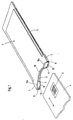
- the adapter shown in Fig. 1 has a housing 1, the Dimensions correspond to those of a Type II PCMCIA plug-in card.
- the Housing 1 is on its narrower end with a PCMCIA connector 2 provided, which - as can be seen from Fig. 3 - is completely housed in the housing 1.
- the housing 1 points to the Plug connection socket 2 opposite end face an insertion slot 3rd for a chip card 4, which is in a laterally open receiving channel 5 transforms.
- the chip card 4 is provided with a flat contact field 6 and can be inserted into the housing 1 in the direction of the double arrow shown or pull out.
- the side walls 7 are in the The area of the insertion slot 3 with frontal bevels 8 and the the receiving channel 5 facing ceiling surface with a sloping Provide allowable recess 9.
- An easy removal of one inserted chip card 4 is replaced by several recessed, Partially circular recesses 10, 10a on the contour of the insertion slot 3 end face and the recesses 10a opposite, surfaces 11 drawn out in the manner of a lower lip, which provide a user with cheap access to chip card 4.
- the Surfaces 11 serve at the same time as support surfaces for the chip card 4 Introduce, making this much easier.
- the surfaces 11 are also included slightly raised clamp cams 12 provided one insert the inserted chip card 4 in the receiving channel 5 and thus insert it Prevent unwanted slipping out.
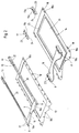
- the housing 1 consists of an upper Cover plate 13 and a lower cover plate 14 through Intermediate elements 15, 16, 17, 17a are connected to one another.
- Sheet metal stamped cover plates 13, 14 are orthogonal angled staples 18, 18a, 18b on during the manufacture of the Intermediate elements 15 to 17a by plastic injection molding them be included so that a simple yet resilient Connection of intermediate elements 15 to 17a and cover elements 13, 14 is ensured despite different materials.
- the intermediate element 15 arranged on the upper cover plate 13 is as formed a substantially U-shaped frame, the legs of their inner contour clamping and guide sections 19, 20 for receiving a Have circuit board 21, while the base of the intermediate element 15 with the previously mentioned inlet slopes 8, the recess 9 and the Recesses 10, 10a is provided. Due to the frame-like design of the intermediate element 15 is a high torsional rigidity of the housing 1 guaranteed.
- the trained as spacer segments Intermediate elements 16 to 17a have one of a chip card 4 approximately appropriate height and thereby form the receiving channel 5.
- the im Area of the insertion slot 3 arranged intermediate element 16 has a Base plate on the front of the contour of the lower cover plate 14 follows and thereby also the previously mentioned surfaces 11, on which the Metal or plastic existing clamping cams 12 as separate parts or are arranged in one piece, forms.
- the in the field of Plug connection socket 2 arranged intermediate elements 17, 17a assign the clamping sections 19 corresponding clamping sections 19a, the together with the aforementioned those with the circuit board 21 electrically Take the connected plug socket 2.
- a chip card 4 front end of the intermediate elements 17, 17a Stops 24 with a contour adapted to the corner shape of a chip card 4 provided that limit the insertion depth of a chip card 4 on the corner.
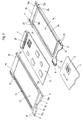
- the lower cover plate 14 has a Recess 25 in which a reinforcing plate 26 is arranged.
- the intermediate elements 16 to 17a are in one piece with one embodiment Bottom plate 27 formed, the 18c with the lower Cover plate 14 is connected.
- the necessary torsional rigidity of the housing 1 on the base plate 27 reached so that on the reinforcing plate 26 and the necessary Indentation 25 in the lower cover plate 14 can be dispensed with if necessary can.
- the adapter described above is suitable for connection to a PCMCIA interface of a computer or the like, the Recording channel 5 for a chip card 4 standardized according to DIN ISO 7816 is designed. That arranged on the top of the chip card 4 Contact field 6 comes with chip card 4 inserted into the adapter to lie opposite contact elements 28, so that contacting is ensured. Because of the suitability of the adapter for a DIN ISO 7816 standardized chip cards 4, in which the card width is the width of the PCMCIA standard conforming to housing 1 is a side Leaving the recording channel 5 indispensable.
- a contingent Impairment of the torsional rigidity and robustness of the housing 1 is by the design of the upper intermediate element 15 as in essential U-shaped frame and the provision of the stiffening plate 26 minimized so that they are largely excluded in practice can be.
- By providing pins 23 and more Corresponding openings 22 will be quick and easy to install Production achieved that is suitable for economical mass production and in the case of a detachable plug-in connection, it is also recycling-related Meets requirements.
Abstract
Description
Die Erfindung betrifft einen Adapter zum Kontaktieren von Chipkarten mit einem vorzugsweise nach PCMCIA-Standard genormten Anschluß eines Datenverarbeitungsgeräts oder dergleichen, bestehend aus einem steckkartenförmigen Gehäuse mit einer oberen und unteren Abdeckplatte, das einen stirnseitigen, in einen Aufnahmekanal mündenden Einschubschlitz für die Aufnahme einer Chipkarte und ein an der gegenüberliegenden Stirnseite angeordnetes Anschlußfeld aufweist, sowie aus einer mit dem Anschlußfeld elektrisch verbundenen Leiterplatte, die sich parallel zum Aufnahmekanal erstreckt und mit Kontaktelementen zum Kontaktieren einer Chipkarte versehen ist.The invention relates to an adapter for contacting chip cards a connection, preferably standardized according to the PCMCIA standard Data processing device or the like, consisting of a card-shaped housing with an upper and lower cover plate, the an insertion slot at the end opening into a receiving channel for the inclusion of a chip card and one on the opposite end has arranged connector panel, and from one with the connector panel electrically connected printed circuit board, which is parallel to the receiving channel extends and with contact elements for contacting a chip card is provided.
Unter einer Chipkarte in voranstehenden Sinne werden kartenförmige Trägerelemente elektronischer Bauteile, insbesondere von Mikroprozessoren, auf denen verschiedene, abrufbare Informationen gespeichert werden können, verstanden. Derartige Chipkarten sind insbesondere im Bereich der Computertechnologie anzutreffen und erfreuen sich einer immer stärker werdenden Verbreitung im Zusammenhang mit der Authentifikation von Subjekten. Neben dieser Verwendung als Identitätskarte für zum Beispiel die Bedienung von Zugangskontrollsystemen, werden Chipkarten derzeit zunehmend auch im bargeldlosen Zahlungsverkehr eingesetzt, wo sie beispielsweise bei Kreditkarten oder im Rahmen von POS-Systemen die Magnetstreifenkarte ablösen.Under a chip card in the above sense card-shaped Carrier elements of electronic components, especially microprocessors, on which various, retrievable information can be stored, Understood. Such chip cards are particularly in the area of Computer technology can be found and enjoy one more and more spreading in connection with the authentication of Subjects. In addition to this use as an identity card for, for example, the Operation of access control systems, chip cards are currently increasingly used in cashless payments, where they for example with credit cards or in the context of POS systems Remove the magnetic stripe card.
Zum Lesen einer Chipkarte sind als Kontaktiereinheit ausgebildete Leseeinheiten bekannt, die in Form eines Adaptersystems beispielsweise ermöglichen, eine Chipkarte an einen nach PCMCIA-Standard genormten Anschluß eines Datenverarbeitungssystems anzuschließen. Die im Stand der Technik hierzu bekannten Adapter weisen eine PCMCIA-Steckanschlußbuchse auf, die mit einem PCMCIA-Steckplatz des Datenverarbeitungssystems eine mechanische und elektrische Kontaktierung bewirkt. Das Auslesen der Chipkarte erfolgt dabei über im Aufnahmekanal für die Chipkarte angeordnete Kontaktelemente, welche dieselbe berührend oder, beispielsweise auf optischem oder magnetischem Weg, berührungslos kontaktieren.To read a chip card are designed as a contacting unit Known reading units, for example in the form of an adapter system enable a chip card to a standardized according to PCMCIA standard Connection of a data processing system. The state of the art Technology known adapters for this have a PCMCIA connector socket with a PCMCIA slot on the data processing system causes mechanical and electrical contacting. Reading the In this case, the chip card is arranged in the receiving channel for the chip card Contact elements which touch the same or, for example, on optical or magnetic path, contactless.
Aus der DE 295 05 678 ist eine Kontaktiereinheit für kartenförmige Trägerelemente elektronischer Baugruppen bekannt, die mit einer Basisplatte mit einer zur planparallelen Aufnahme eines kartenförmigen Trägerelementes geeigneten Größe, wenigstens einer im wesentlichen parallel zur Basisplatte angeordneten Leiterplatte mit Kontaktelementen für die elektronischen Baugruppen des Trägerelementes an ihrer Oberfläche sowie mit einem an einer Kante der Basisplatte angeordneten Anschlußfeld versehen ist. Ein zur Basisplatte im wesentlichen deckungsgleiches, plattenförmiges Abdeckelement bildet mit der Leiterplatte einen schlitzartigen Einschubkanal und ist im Bereich des Anschlußfeldes und der dieser gegenüberliegenden Ecken an der Basisplatte befestigt. Die Befestigung im Bereich des Anschlußfeldes erfolgt dabei über zwei seitlich des Anschlußfeldes verlaufende Stege, die einstückig mit der Basisplatte und dem Abdeckelement verbunden sind. Als Nachteil hierbei erweist sich, daß eine derartige Bauform nur mit großem wirtschaftlichen Aufwand herstellbar ist und sich daher nur bedingt für eine billige Massenproduktion eignet Ursächlich hierfür ist die einstückige Bauweise von Basisplatte und Abdeckelement, die eine zeitaufwendige und damit ungünstige Montage mit sich bringt. Zudem ist die Auswahl der verwendbaren Materialien beschränkt, da das Abdeckelement über die Stege um das Anschlußfeld auf die Unterseite der Kontaktiereinheit umgebogen wird, so daß eine gewisse Biegsamkeit für ein zu verwendendes Material vorausgesetzt sein muß.From DE 295 05 678 a contact unit for card-shaped Carrier elements of electronic assemblies known with a base plate with one for the plane-parallel recording of a card-shaped support element suitable size, at least one substantially parallel to the base plate arranged circuit board with contact elements for the electronic Assemblies of the support element on their surface and with one on one Edge of the base plate arranged connector panel is provided. One for Base plate essentially congruent, plate-shaped cover element forms a slot-like insertion channel with the circuit board and is in the area of the connector panel and the corners opposite this at the Base plate attached. The attachment in the area of the connection panel takes place thereby over two webs running to the side of the connection field, which are in one piece are connected to the base plate and the cover element. As a disadvantage here it turns out that such a design only with large is economical to produce and is therefore only conditionally for one cheap mass production is suitable The reason for this is the one-piece Construction of the base plate and cover element, which is a time-consuming and so that unfavorable assembly entails. In addition, the selection of the usable materials limited because the cover over the webs bent around the connector panel on the underside of the contact unit is so that a certain flexibility for a material to be used must be assumed.
Der Erfindung liegt die Aufgabe zugrunde, einen Adapter zum Kontaktieren von Chipkarten mit einem vorzugsweise nach PCMCIA-Standard genormten Anschluß eines Datenverarbeitungsgeräts oder dergleichen dahingehend weiterzubilden, daß sich eine einfache und kostengünstige Herstellung erreichen läßt, die eine wirtschaftliche Massenproduktion im Hinblick auf die zunehmend umfangreichere Verwendung vorbeschriebener Kartensysteme gewährleistet.The invention is based on the object of developing an adapter for contacting chip cards with a connection of a data processing device or the like, preferably standardized according to the PCMCIA standard, in such a way that simple and inexpensive production can be achieved, which is economical in mass production in view of the increasingly extensive use guaranteed card systems.
Die Aufgabe ist bei einem Adapter der eingangs genannten Art erfindungsgemäß dadurch gelöst, daß die obere und untere Abdeckplatten zwei getrennte, deckungsgleiche Bauteile sind, und daß zwischen oberer und unterer Abdeckplatte wenigstens ein Zwischenelement vorgesehen ist, welche diese miteinander verbindete.The object is attained by an adapter of the type mentioned according to the invention in that the top and bottom cover are two separate congruent components, and that an intermediate element is provided between the upper and lower cover plate, at least that this verbindete each other.
Ein solchermaßen ausgestalteter Adapter läßt sich einfach und kostengünstig herstellen und gestattet daher eine Massenproduktion im zuvor erwähnten Sinn. Dies ist darauf zurückzuführen, daß sich zum einen aufgrund der zweiteiligen Ausgestaltung mit oberer und unterer Abdeckplatte eine einfache Montage ergibt und zum anderen infolge des Verbindens der Abdeckplatten über die Zwischenelemente eine bedarfsgerechte Verwendung auch unterschiedlichster Materialien mit geringem fertigungstechnischen Aufwand erreichen läßt. Mögliche Anwendungsgebiete für Letztgenanntes können beispielsweise in der bedarfsabhängigen Verwendung nichtleitender oder leitender Materialien für die Abdeckplatten hinsichtlich einer geforderten Abschirmung, statischen Ableitung und dergleichen bestehen.An adapter designed in this way is simple and inexpensive manufacture and therefore allows mass production in the aforementioned Sense. This is due to the fact that, on the one hand, due to the two-part design with an upper and lower cover plate a simple Assembly results and secondly due to the connection of the cover plates a need-based use also via the intermediate elements different materials with little manufacturing effort can be achieved. Possible areas of application for the latter can for example in the need-based use of non-conductive or conductive materials for the cover plates with regard to a required Shielding, static dissipation and the like exist.
In einer bevorzugten Ausführungsform ist die obere Abdeckplatte mit einem oberen und die untere Abdeckplatte mit unteren Zwischenelementen versehen, die an ihren gegenüberliegenden Berührungsflächen miteinander verbunden sind. Dies bietet den Vorteil, daß die jeweiligen Abdeckplatten und dazugehörigen Zwischenelemente vorgefertigt werden können, so daß nach erfolgter Bestückung mit Leiterplatte und Anschlußfeld eine einfache Verbindung der gleichartigen oberen und unteren Zwischenelemente möglich ist. Zu diesem Zweck wird weiterhin vorgeschlagen, daß an dem oberen und den unteren Zwischenelementen korrespondierend ausgebildete Zapfen und Öffnungen angeordnet sind, um eine einfache und schnelle Zentrierung der aufeinander anzuordnenden Zwischenelemente zu erzielen, die anschließend mittels Ultraschallschweißen, Kleben oder sonstigem Stoffschluß miteinander verbunden werden können. In a preferred embodiment, the upper cover plate is with a provide upper and lower cover plates with lower intermediate elements, which are connected to each other at their opposite contact surfaces are. This has the advantage that the respective cover plates and associated intermediate elements can be prefabricated, so that after completed with a simple circuit board and connector panel Connection of the same upper and lower intermediate elements possible is. For this purpose it is further proposed that at the top and the lower intermediate elements correspondingly designed pins and Openings are arranged for easy and quick centering of the to achieve intermediate elements to be arranged, which then by means of ultrasonic welding, gluing or other material bonding with each other can be connected.
Gemäß einer alternativen Weiterbildung der Erfindung sind das obere und die unteren Zwischenelemente mit korrespondierend ausgebildeten Zapfen und Öffnungen in Form einer Steckverbindung versehen und lösbar miteinander verbunden. Auf diese Weise ist eine einfache Trennung von oberer und unterer Abdeckplatte über die Zwischenelemente sichergestellt, was ein einfaches Zerlegen eines Adapters beispielsweise im Zusammenhang mit Recycling gewährleistet.According to an alternative development of the invention, the upper and the lower intermediate elements with correspondingly designed pins and Provide openings in the form of a plug connection and detachable with each other connected. In this way there is a simple separation of upper and lower cover plate over the intermediate elements ensures what a easy disassembly of an adapter, for example in connection with Recycling guaranteed.
Gemäß einem weiteren vorteilhaften Merkmal sind das obere und die unteren Zwischenelemente Kunststoff-Spritzteile, die mittels Spritzgießen an der jeweiligen oberen und unteren Abdeckplatte befestigbar sind, so daß sich sowohl eine einfache und kostengünstige Herstellung der Zwischenelemente als auch eine zuverlässige Verbindung letztgenannter mit den Abdeckplatten erzielen läßt. Zweckmäßigerweise sind hierzu die obere und die untere Abdeckplatte jeweils mit angeformten Krampen versehen, die in dem oberen und den jeweiligen unteren Zwischenelementen eingegossen sind, um eine zuverlässige, stoffschlüssige Verbindung zu gewährleisten.According to a further advantageous feature, the upper and lower ones Intermediate elements injection molded plastic parts by injection molding on the respective upper and lower cover plate can be fastened so that both simple and inexpensive manufacture of the intermediate elements as well as a reliable connection of the latter with the cover plates can be achieved. For this purpose, the upper and the lower are expedient Cover plate each provided with molded cramps, which in the upper and the respective lower intermediate elements are cast to a to ensure reliable, integral connection.
Gemäß einem weiteren Merkmal der Erfindung ist das obere Zwischenelement als im wesentlichen U-förmiger Rahmen ausgebildet, dessen Außenkontur der der oberen Abdeckplatte folgt und dessen Innenkontur Klemm- und Führungsabschnitte zur Aufnahme der Leiterplatte zwischen den beiden Schenkeln des Rahmens aufweist. Dies bietet den Vorteil einer Erhöhung der Verwindungssteifigkeit des Adapters, indem zum Beispiel die Schenkel des Rahmens Teile der seitlichen Wandungen des Gehäuses bilden. Durch die Ausgestaltung der Innenkontur der Schenkeln mit Klemm- und Führungsabschnitte zur Aufnahme der Leiterplatte wird zudem einen hohe Funktionsintegration erreicht. Um eine möglichst genaue Führung und sichere Kontaktierung einer Chipkarte im Adapter sicherzustellen - was eine annähernd gleiche Höhe von Chipkarte und Aufnahmekanal erfordert -, gleichzeitig aber auch ein einfaches und schnelles Einführen einer Chipkarte in den Adapter zu gewährleisten, ist gemäß einer weiteren vorteilhaften Ausgestaltung der Erfindung die dem Aufnahmekanal zugewandte Fläche der im Bereich des Einschubschlitzes angeordneten Basis des Rahmens an einer Seite mit einer flächigen Ausnehmung versehen. Dies gestattet ein etwas schräges und damit einfaches Einführen einer Chipkarte in den Einschubschlitz des Adapters.According to a further feature of the invention, the upper intermediate element formed as a substantially U-shaped frame, the outer contour of the the upper cover plate follows and its inner contour clamping and Guide sections for receiving the circuit board between the two Has legs of the frame. This offers the advantage of increasing the Torsional rigidity of the adapter, for example by the legs of the Frame form parts of the side walls of the housing. Through the Design of the inner contour of the legs with clamping and Guide sections for receiving the circuit board will also be high Functional integration achieved. To ensure the most accurate and safe guidance Ensure contacting a chip card in the adapter - what a requires approximately the same height of chip card and recording channel -, but at the same time also a simple and quick insertion of a chip card in To ensure the adapter is according to another advantageous Embodiment of the invention, the surface of the receiving channel facing in the region of the insertion slot arranged base of the frame on a Provide side with a flat recess. This allows something slanted and thus easy insertion of a chip card into the slot of the adapter.
Von besonderem Vorteil ist es, wenn die unteren Zwischenelemente annähernd die Höhe einer Chipkarte aufweisende Abstandssegmente sind, die einerseits im in Einschubrichtung einer Chipkarte vorderen Bereich des Gehäuses geschlossene seitliche Wandungen des Einschubschlitzes bilden und andererseits unter seitlichem Freilassen des sich an den Einschubschlitz anschließenden Aufnahmekanals beidseitig des Anschlußfelds angeordnet sind. Auf diese Weise wird eine sichere Führung und Kontaktierung einer Chipkarte im Adapter sichergestellt. Gleichzeitig ermöglicht das seitliche Freilassen nach PCMCIA-Standard vom Typ I, II, III oder IV genormte Abmessungen des steckkartenförmigen Gehäuses.It is particularly advantageous if the lower intermediate elements are approximately the height of a chip card having spacing segments that on the one hand in the front area of the chip card in the direction of insertion Form housing closed side walls of the slot and on the other hand, leaving the slot at the side subsequent receiving channel arranged on both sides of the connector panel are. In this way, safe guidance and contacting a Chip card ensured in the adapter. At the same time, the side enables Release according to PCMCIA standard of type I, II, III or IV Dimensions of the card-shaped housing.
Um die Robustheit des Adapters zu erhöhen, ist gemäß einer weiteren vorteilhaften Weiterbildung der Erfindung das im Bereich des Einschubschlitzes angeordnete Abstandssegment einstückig mit einer Bodenplatte ausgebildet, deren Außenkontur der der unteren Abdeckplatte entspricht. Zu dem gleichen Zweck wird weiterhin vorgeschlagen, daß die untere Abdeckplatte mit einer Vertiefung versehen ist, in der eine vorzugsweise metallene Verstärkungsplatte angeordnet ist. In einer bevorzugten Ausführungsform der Erfindung sind die Abstandssegmente hierzu einstückig mit einer zur unteren Abdeckplatte deckungsgleichen Bodenplatte ausgebildet. Dies besitzt den Vorteil einer zeitgleichen Herstellung von Abdeckplatte und verstärkend wirkender Bodenplatte, so daß ein zusätzliches Anbringen der Verstärkungsplatte entfallen kann.To increase the robustness of the adapter, according to another advantageous development of the invention in the area of the slot arranged spacer segment formed in one piece with a base plate, whose outer contour corresponds to that of the lower cover plate. At the same Purpose is also proposed that the lower cover plate with a Depression is provided, in which a preferably metallic Reinforcing plate is arranged. In a preferred embodiment of the According to the invention, the spacer segments are in one piece with one to the lower one Cover plate formed congruent base plate. This owns the Advantage of simultaneous production of cover plate and reinforcement acting base plate, so that an additional attachment of the Reinforcing plate can be omitted.
Gemäß einem weiteren Merkmal der Erfindung weisen die beidseitig des Anschlußfeldes angeordneten Abstandssegmente an ihren gegenüberliegenden Innenflächen Klemmabschnitte zur Fixierung des Anschlußfeldes auf, so daß eine einfache und schnelle Montage gewährleistet ist. Zweckmäßigerweise ist das im Bereich des Einschubschlitzes angeordnete Abstandssegment mit Einlaufschrägen für eine einzuführende Chipkarte und die beidseitig des Anschlußfeldes angeordneten Abstandssegmente mit die Einstecktiefe einer Chipkarte eckseitig begrenzenden Anschlägen, welche eine an die Eckenform der Chipkarte angepaßte Kontur aufweisen, versehen. Durch diese Maßnahme ist ein einfaches Einführen einer Chipkarte und ein sicherer Sitz derselben im Aufnahmekanal des Adapters gewährleistet.According to a further feature of the invention, the on both sides of the Terminal field arranged spacing segments on their opposite Inner surfaces of clamping sections for fixing the connection panel, so that simple and quick installation is guaranteed. It is expedient the spacing segment arranged in the region of the insertion slot Inlet bevels for a chip card to be inserted and the on both sides of the Connection field arranged spacing segments with the insertion depth of one Chip card stops on the corner, which have a shape at the corner have the contour adapted to the chip card. By this measure is a simple insertion of a chip card and a secure fit of the same in the Receiving channel of the adapter guaranteed.
Um eine ergonomisch günstige Handhabung des Adapters zu gewährleisten, wird gemäß einem weiteren vorteilhaften Merkmal der Erfindung vorgeschlagen, daß die obere Abdeckplatte an der den Einschubschlitz aufweisenden Stirnseite eine durch mehrere zurückspringende, teilkreisförmige Aussparungen gebildete Kontur aufweist. Die ergonomische Handhabung wird weiterhin dadurch begünstigt, daß die untere Abdeckplatte an der den Einschubschlitz aufweisenden Stirnseite in zumindest einem der beiden äußeren, teilkreisförmigen Aussparungen der oberen Abdeckplatte gegenüberliegenden Bereich eine nach Art einer Unterlippe hervorgezogene Fläche aufweist, auf der wenigstens ein Klemmnocken angeordnet ist, durch den zusammen mit den an den Abstandssegmenten ausgebildeten Anschlägen die Chipkarte sicherbar ist. Dies trägt auch dazu bei, daß die Kontaktsicherheit erheblich erhöht wird.To ensure ergonomic handling of the adapter, is according to another advantageous feature of the invention suggested that the top cover plate on the insertion slot having a front face by several recessed, partially circular Has recesses formed contour. The ergonomic handling further favored in that the lower cover plate on the Insertion slot end face in at least one of the two outer, part-circular recesses of the upper cover plate opposite area pulled out like a lower lip Has surface on which at least one clamping cam is arranged by the together with the stops formed on the spacer segments the chip card can be secured. This also helps to ensure contact security is significantly increased.
Schließlich wird vorgeschlagen, daß die obere und die untere Abdeckplatte aus Metall gefertigt sind, um neben einer guten Abschirmung auch eine robuste und langlebige Bauweise zu erzielen.Finally, it is proposed that the upper and lower cover plates are made of metal, in addition to a good shielding to achieve robust and durable construction.
Weitere Merkmale und Vorteile des Gegenstandes der Erfindung ergeben sich aus der nachfolgenden Beschreibung eines bevorzugten Ausführungsbeispieles. In den zugehörigen Zeichnungen zeigen:
- Fig. 1
- in einer perspektivischen Ansicht einen Adapter und eine Chipkarte;
- Fig. 2
- eine Explosionsdarstellung von einer oberen und einer unteren Abdeckplatte mit jeweils zugehörigen Zwischenelementen;
- Fig. 3
- in einer perspektivischen Ansicht eine mit einem Anschlußfeld versehene Leiterplatte sowie mit den Zwischenelementen verbundene obere und untere Abdeckplatte und
- Fig. 4
- eine Explosionsdarstellung von oberer und unterer Abdeckplatte mit zugehörigen Zwischenelementen in einer alternativen Ausführungsform.
- Fig. 1
- in a perspective view an adapter and a chip card;
- Fig. 2
- an exploded view of an upper and a lower cover plate with associated intermediate elements;
- Fig. 3
- in a perspective view of a printed circuit board provided with a connection field and connected to the intermediate elements upper and lower cover plate and
- Fig. 4
- an exploded view of the upper and lower cover plate with associated intermediate elements in an alternative embodiment.
Der in Fig. 1 dargestellte Adapter weist ein Gehäuse 1 auf, dessen
Abmessungen denen einer PCMCIA-Steckkarte vom Typ II entsprechen. Das
Gehäuse 1 ist an seiner schmäleren Stirnseite mit einer PCMCIA-Steckanschlußbuchse
2 versehen, die - wie aus Fig. 3 ersichtlich -
vollkommen im Gehäuse 1 untergebracht ist. Das Gehäuse 1 weist an der der
Steckanschlußbuchse 2 gegenüberliegenden Stirnseite einen Einschubschlitz 3
für eine Chipkarte 4 auf, der in einen seitlich offenen Aufnahmekanal 5
übergeht. Die Chipkarte 4 ist mit einem flächigen Kontaktfeld 6 versehen und
läßt sich in Richtung des gezeigten Doppelpfeiles in das Gehäuse 1 einführen
bzw. herausziehen.The adapter shown in Fig. 1 has a housing 1, the
Dimensions correspond to those of a Type II PCMCIA plug-in card. The
Housing 1 is on its narrower end with a
Zum besseren Einführen der Chipkarte 4 sind die seitlichen Wandungen 7 im
Bereich des Einschubschlitzes 3 mit stirnseitigen Einlaufschrägen 8 und die
dem Aufnahmekanal 5 zugewandte Deckenfläche mit einer ein schräges
Einführen gestattenden Ausnehmung 9 versehen. Eine leichte Entnahme einer
eingeschobenen Chipkarte 4 wird durch mehrere zurückspringende,
teilkreisförmige Aussparungen 10, 10a an der Kontur der den Einschubschlitz
3 aufweisenden Stirnseite sowie den Aussparungen 10a gegenüberliegenden,
nach Art einer Unterlippe hervorgezogenen Flächen 11 gewährleistet, die
einem Benutzer einen günstigen Zugriff zur Chipkarte 4 ermöglichen. Die
Flächen 11 dienen gleichzeitig als Abstützflächen der Chipkarte 4 beim
Einführen, wodurch dieses erheblich vereinfacht wird. Um eine Verriegelung
einer eingeschobenen Chipkarte 4 zu erreichen, sind die Flächen 11 zudem mit
geringfügig hochstehenden Klemmnocken 12 versehen, die eine
eingeschobene Chipkarte 4 im Aufnahmekanal 5 festsetzen und damit ein
ungewolltes Herausrutschen verhindern.For better insertion of the
Wie aus Fig. 2 ersichtlich ist, besteht das Gehäuse 1 aus einer oberen
Abdeckplatte 13 und einer unteren Abdeckplatte 14, die durch
Zwischenelemente 15, 16, 17, 17a miteinander verbunden sind. Die als
Blechstanzteile gefertigten Abdeckplatten 13, 14 weisen orthogonal
abgewinkelte Krampen 18, 18a, 18b auf, die während der Herstellung der
Zwischenelemente 15 bis 17a durch Kunststoff-Spritzgießen von diesen
eingeschlossen werden, so daß eine einfache, aber dennoch belastbare
Verbindung von Zwischenelementen 15 bis 17a und Abdeckelementen 13, 14
trotz unterschiedlicher Materialien sichergestellt ist.As can be seen from Fig. 2, the housing 1 consists of an
Das an der oberen Abdeckplatte 13 angeordnete Zwischenelement 15 ist als
ein im wesentlichen U-förmiger Rahmen ausgebildet, dessen Schenkeln an
ihrer Innenkontur Klemm- und Führungsabschnitte 19, 20 zur Aufnahme einer
Leiterplatte 21 aufweisen, während die Basis des Zwischenelements 15 mit
den zuvor erwähnten Einlaufschrägen 8, der Ausnehmung 9 sowie den
Aussparungen 10, 10a versehen ist. Durch die rahmenartige Ausgestaltung
des Zwischenelements 15 ist eine hohe Verwindungssteifigkeit des Gehäuses
1 gewährleistet.The
An der dem Aufnahmekanal 5 zugewandten Unterseite des Zwischenelements
15 sind im Seitenbereich der Basis und im Endbereich der Schenke Öffnungen
22 vorgesehen, die mit korrespondierend ausgebildeten Zapfen 23 an den
gegenüberliegenden Zwischenelementen 16 bis 17a fluchten und bei Montage
des Adapters in diese eingreifen. Die als Abstandssegmente ausgebildeten
Zwischenelemente 16 bis 17a weisen eine der einer Chipkarte 4 annähernd
entsprechende Höhe auf und bilden dadurch den Aufnahmekanal 5. Das im
Bereich des Einschubschlitzes 3 angeordnete Zwischenelement 16 weist eine
Bodenplatte auf, die an ihrer Stirnseite der Kontur der unteren Abdeckplatte
14 folgt und dadurch auch die zuvor erwähnten Flächen 11, auf denen die aus
Metall oder Kunststoff bestehenden Klemmnocken 12 als separate Teile oder
einstückig ausgebildet angeordnet sind, bildet. Die im Bereich der
Steckanschlußbuchse 2 angeordneten Zwischenelemente 17, 17a weisen zu
den Klemmabschnitten 19 korrespondierende Klemmabschnitte 19a auf, die
zusammen mit den zuvorgenannten die mit der Leiterplatte 21 elektrisch
verbundene Steckanschlußbuchse 2 aufnehmen. An der in Einschubrichtung
einer Chipkarte 4 vorderen Stirnseite der Zwischenelemente 17, 17a sind
Anschläge 24 mit einer an die Eckenform einer Chipkarte 4 angepaßten Kontur
vorgesehen, die die Einstecktiefe einer Chipkarte 4 eckseitig begrenzen.On the underside of the intermediate element facing the receiving
Wie aus Fig. 4 zu entnehmen ist, weist die untere Abdeckplatte 14 eine
Vertiefung 25 auf, in der eine Verstärkungsplatte 26 angeordnet ist. Die
Befestigung der aus Metall bestehenden Verstärkungsplatte 26, welche die
Steifigkeit des Adapters erheblich erhöht, erfolgt dabei über
Ultraschallschweißen oder Kleben. In der in Fig. 4 gezeigten alternativen
Ausführungsform sind die Zwischenelemente 16 bis 17a einstückig mit einer
Bodenplatte 27 ausgebildet, die über Krampen 18c mit der unteren
Abdeckplatte 14 verbunden ist. Bei dieser alternativen Ausführungsform wird
die notwendige Verwindungssteifigkeit des Gehäuses 1 über die Bodenplatte
27 erreicht, so daß auf die Verstärkungsplatte 26 sowie die dafür erforderliche
Vertiefung 25 in der unteren Abdeckplatte 14 bei Bedarf verzichtet werden
kann.As can be seen from Fig. 4, the
Bei Montage des Adapters werden die mit den Zwischenelementen 15 bis 17a
versehenen obere und untere Abdeckplatten 13, 14 derart übereinander
gelegt, daß die Zapfen 23 in die Öffnungen 22 eingreifen und gleichzeitig die
Leiterplatte 21 in den Führungsabschnitten 20 und die Steckanschlußbuchse 2
in den Klemmabschnitten 19, 19a zu liegen kommen. Die durch das
Ineinandergreifen der Zapfen 23 und der Öffnungen 22 bereits zentrierten
Zwischenelemente 15 bis 17a können dann mittels Kleben oder
Ultraschallschweißen verbunden werden. Bei Ausgestaltung der Zapfen 23
und der korrespondierenden Öffnungen 22 in Form einer Steckverbindung
kann außer der montagegünstigen Zentrierung der aufeinander anzuordnenden
Zwischenelemente 15 bis 17a auch eine endgültige Fixierung dieser erreicht
werden, die sich hinsichtlich eines recyclingbedingten Zerlegens auszeichnet.When mounting the adapter with the
Der zuvor beschriebene Adapter eignet sich für den Anschluß an eine
PCMCIA-Schnittstelle eines Computers oder dergleichen, wobei der
Aufnahmekanal 5 für eine nach DIN ISO 7816 genormte Chipkarte 4
ausgestaltet ist. Das an der Oberseite der Chipkarte 4 angeordnete
Kontaktfeld 6 kommt bei in den Adapter eingeschobener Chipkarte 4
gegenüber von Kontaktelementen 28 zu liegen, so daß eine Kontaktierung
sichergestellt ist. Aufgrund der Eignung des Adapters für eine nach DIN ISO
7816 genormte Chipkarten 4, bei der die Kartenbreite der Breite des nach
PCMCIA-Standard genormten Gehäuses 1 entspricht, ist ein seitliches
Offenlassen des Aufnahmekanals 5 unerläßlich. Eine dadurch bedingte
Beeinträchtigung der Verwindungssteifigkeit und Robustheit des Gehäuses 1
wird durch die Ausgestaltung des oberen Zwischenelements 15 als im
wesentlichen U-förmiger Rahmen sowie das Vorsehen der Versteifungsplatte
26 derart minimiert, daß sie in der Praxis weitestgehend ausgeschlossen
werden kann. Durch das Vorsehen von Zapfen 23 und dazu
korrespondierenden Öffnungen 22 wird eine schnelle und montagerechte
Herstellung erzielt, die sich für eine wirtschaftliche Massenfertigung eignet
und bei Ausgestaltung als lösbare Steckverbindung zudem recyclingbedingten
Anforderungen Rechnung trägt. The adapter described above is suitable for connection to a
PCMCIA interface of a computer or the like, the
- 11
- Gehäusecasing
- 22nd
- SteckanschlußbuchsePlug connection socket
- 33rd
- EinschubschlitzSlot
- 44th
- ChipkarteSmart card
- 55
- AufnahmekanalRecording channel
- 66
- KontaktfeldContact field
- 77
- WandungWall
- 88th
- EinlaufschrägeEntry slope
- 99
- AusnehmungRecess
- 1010th
- AussparungRecess
- 10a10a
- AussparungRecess
- 1111
- Flächesurface
- 1212th
- KlemmnockenClamping cams
- 1313
- obere Abdeckplatteupper cover plate
- 1414
- untere Abdeckplattelower cover plate
- 1515
- ZwischenelementIntermediate element
- 1616
- ZwischenelementIntermediate element
- 1717th
- ZwischenelementIntermediate element
- 17a17a
- ZwischenelementIntermediate element
- 1818th
- KrampenCramps
- 18a18a
- KrampenCramps
- 18b18b
- KrampenCramps
- 18c18c
- KrampenCramps
- 1919th
- KlemmabschnittClamping section
- 19a19a
- KlemmabschnittClamping section
- 2020th
- FührungsabschnittGuide section
- 2121
- LeiterplatteCircuit board
- 2222
- Öffnungopening
- 2323
- ZapfenCones
- 2424th
- Anschlagattack
- 2525th
- Vertiefungdeepening
- 2626
- VerstärkungsplatteReinforcement plate
- 2727
- BodenplatteBase plate
- 2828
- KontaktelementeContact elements
Claims (17)
dadurch gekennzeichnet,
daß die obere und untere Abdeckplatte zwei getrennte, deckungsgleiche Bauteile sind, und daß zwischen oberer und unterer Abdeckplatte wenigstens ein Zwischenelement vorgesehen ist, welche diese miteinander verbindet.Adapter for contacting chip cards (4) with a connection of a data processing device or the like, preferably standardized according to the PCMCIA standard, consisting of a plug-in card-shaped housing (1) with an upper and lower cover plate (13, 14) 5) opening insertion slot (3) for receiving a chip card (4) and a connection panel (2) arranged on the opposite end face, and from a printed circuit board (21) electrically connected to the connection panel (2), which is parallel to the receiving channel ( 5) extends and is provided with contact elements (28) for contacting a chip card (4),
characterized,
that the upper and lower cover plate are two separate, congruent components, and that at least one intermediate element is provided between the upper and lower cover plate, which connects them together.
Applications Claiming Priority (2)
| Application Number | Priority Date | Filing Date | Title |
|---|---|---|---|
| DE29722142U DE29722142U1 (en) | 1997-12-16 | 1997-12-16 | Adapter for contacting chip cards |
| DE29722142U | 1997-12-16 |
Publications (3)
| Publication Number | Publication Date |
|---|---|
| EP0924640A2 true EP0924640A2 (en) | 1999-06-23 |
| EP0924640A3 EP0924640A3 (en) | 2000-10-11 |
| EP0924640B1 EP0924640B1 (en) | 2005-05-18 |
Family
ID=8049992
Family Applications (1)
| Application Number | Title | Priority Date | Filing Date |
|---|---|---|---|
| EP98122337A Expired - Lifetime EP0924640B1 (en) | 1997-12-16 | 1998-11-25 | Adapter for contacting of smart cards |
Country Status (4)
| Country | Link |
|---|---|
| US (1) | US6272017B1 (en) |
| EP (1) | EP0924640B1 (en) |
| JP (1) | JP2000003416A (en) |
| DE (2) | DE29722142U1 (en) |
Cited By (3)
| Publication number | Priority date | Publication date | Assignee | Title |
|---|---|---|---|---|
| EP1143371A2 (en) * | 2000-04-04 | 2001-10-10 | J.S.T. Mfg. Co., Ltd. | Electrical connector |
| WO2003107254A1 (en) * | 2002-06-13 | 2003-12-24 | Stocko Contact Gmbh & Co. Kg | Chipcard reader in pc-card format |
| AU2009200080B2 (en) * | 1999-11-01 | 2011-09-22 | Respironics, Inc | Method and apparatus for monitoring and controlling a medical device |
Families Citing this family (31)
| Publication number | Priority date | Publication date | Assignee | Title |
|---|---|---|---|---|
| US6522299B2 (en) * | 1999-04-08 | 2003-02-18 | Cypress Semiconductor Corp. | PC card retractable antenna |
| JP2000305662A (en) | 1999-04-23 | 2000-11-02 | Jst Mfg Co Ltd | Adapter for card connection |
| DE29909222U1 (en) * | 1999-05-28 | 1999-08-05 | Stocko Contact Gmbh & Co Kg | PC card chip card reader |
| JP2000357548A (en) * | 1999-06-16 | 2000-12-26 | Kel Corp | Connector for card |
| US6470284B1 (en) * | 1999-08-05 | 2002-10-22 | 02 Micro International Limited | Integrated PC card host controller for the detection and operation of a plurality of expansion cards |
| JP5201543B2 (en) * | 2000-09-06 | 2013-06-05 | 日立マクセル株式会社 | IC card reader / writer |
| US6498731B1 (en) * | 2000-10-18 | 2002-12-24 | Compaq Computer Corporation | System for protecting electronic components |
| US6760229B2 (en) * | 2000-10-18 | 2004-07-06 | Hewlett-Packard Development Company, L.P. | System for protecting electronic components |
| WO2002059831A1 (en) * | 2001-01-26 | 2002-08-01 | Sony Corporation | Ic card and ic card adaptor |
| US6461170B1 (en) * | 2001-05-17 | 2002-10-08 | 3Com Corporation | Stacked electronic integrated card assembly with multi-function shared interface |
| JP3894031B2 (en) * | 2001-05-22 | 2007-03-14 | 株式会社村田製作所 | Card type portable device |
| DE20117188U1 (en) * | 2001-10-19 | 2002-01-03 | Stocko Contact Gmbh & Co Kg | Adapter for contacting chip cards |
| TW534499U (en) * | 2001-11-07 | 2003-05-21 | Hon Hai Prec Ind Co Ltd | Smart card adapter |
| DE20201237U1 (en) * | 2002-01-28 | 2002-06-13 | Scm Microsystems Gmbh | Smart card reader |
| JP4019965B2 (en) * | 2003-02-10 | 2007-12-12 | ソニー株式会社 | IC card adapter device |
| US20040229511A1 (en) * | 2003-05-16 | 2004-11-18 | Yuan-Hua Chen | Memory card adapter |
| JP2005005104A (en) * | 2003-06-11 | 2005-01-06 | Hirose Electric Co Ltd | Electric connector assembly for cards |
| FR2858866B1 (en) * | 2003-08-14 | 2005-12-02 | Datacard Inc | ADAPTER ELEMENT FOR PROGRAMMABLE ELECTRONIC SUPPORTS AND USE IN A UNIVERSAL PERSONALIZATION MACHINE |
| US20050083662A1 (en) * | 2003-10-15 | 2005-04-21 | Huei-Chen Wong | Wireless LAN PC card casing |
| JP4485173B2 (en) * | 2003-11-19 | 2010-06-16 | モレックス インコーポレイテド | Memory card adapter |
| US7102883B2 (en) * | 2003-12-19 | 2006-09-05 | Hewlett-Packard Development Company, L.P. | Memory package |
| DE202004000179U1 (en) * | 2004-01-09 | 2004-03-18 | Stocko Contact Gmbh & Co. Kg | Contacting unit for a card-shaped carrier element of electronic assemblies |
| US20050213299A1 (en) * | 2004-03-29 | 2005-09-29 | Hardt Thomas T | Memory package |
| US7097512B1 (en) * | 2005-11-07 | 2006-08-29 | Chip Hope Co., Ltd. | Mini memory card adapter |
| DE102005061688A1 (en) * | 2005-12-21 | 2007-07-05 | Stocko Contact Gmbh & Co. Kg | contacting |
| US7070453B1 (en) * | 2006-01-03 | 2006-07-04 | Kingconn Technology Co., Ltd. | Slim five-in-one memory card adapter |
| US7505277B2 (en) | 2007-01-31 | 2009-03-17 | Hewlett-Packard Development Company, L.P. | System comprising a slot configurable to receive a device having an interface type that differs from the interface type of the slot |
| WO2010099305A2 (en) * | 2009-02-27 | 2010-09-02 | Dualsonic, Llc | Electronic housing, assemblies therefor and methods of making same |
| USD642578S1 (en) * | 2009-09-30 | 2011-08-02 | Sony Corporation | Memory card adapter |
| JP5523243B2 (en) * | 2010-08-06 | 2014-06-18 | 日本圧着端子製造株式会社 | Card connector |
| EP2421243A1 (en) | 2010-08-20 | 2012-02-22 | SmarDTV S.A. | Method for assembly of a housing for an interface device comprising a conditional access module |
Citations (4)
| Publication number | Priority date | Publication date | Assignee | Title |
|---|---|---|---|---|
| EP0675456A1 (en) * | 1994-03-21 | 1995-10-04 | Framatome Connectors International | Casing for IC-card reader |
| EP0704813A2 (en) * | 1994-09-29 | 1996-04-03 | Kabushiki Kaisha Toshiba | Ic card information processing apparatus |
| EP0724226A2 (en) * | 1995-01-24 | 1996-07-31 | Kabushiki Kaisha Toshiba | IC card reader/writer |
| WO1997039418A1 (en) * | 1996-04-18 | 1997-10-23 | Itt Manufacturing Enterprises, Inc. | Electronic connection box for a personal computer with a smart card connector |
Family Cites Families (12)
| Publication number | Priority date | Publication date | Assignee | Title |
|---|---|---|---|---|
| CA2083017C (en) | 1992-11-16 | 1999-02-09 | Alan Walter Ainsbury | Tandem circuit cards |
| DE9304034U1 (en) | 1993-03-18 | 1993-09-23 | Zenke Werner | ADAPTER FOR RECORDING SEVERAL PCMCIA STANDARD CARD |
| US5397857A (en) | 1993-07-15 | 1995-03-14 | Dual Systems | PCMCIA standard memory card frame |
| US5457601A (en) * | 1993-12-08 | 1995-10-10 | At&T Corp. | Credit card-sized modem with modular DAA |
| GB9400344D0 (en) | 1994-01-10 | 1994-03-09 | Amp Gmbh | Smart card connector |
| US5748443A (en) | 1995-01-04 | 1998-05-05 | International Business Machines Corporation | Mating adapter between a module and chassis of a computer processing system |
| DE29505678U1 (en) | 1995-04-01 | 1995-06-14 | Stocko Metallwarenfab Henkels | Contact unit for card-shaped carrier elements |
| US5574628A (en) | 1995-05-17 | 1996-11-12 | The Whitaker Corporation | Rigid PCMCIA frame kit |
| TW310872U (en) | 1995-09-22 | 1997-07-11 | View Technology Co Ltd 3 | Improved structure of housing cover for PCMCIA card |
| JP3292803B2 (en) * | 1995-12-28 | 2002-06-17 | 山一電機株式会社 | Card-in type connector |
| DE29622184U1 (en) | 1996-12-20 | 1997-02-27 | Siemens Ag | Device for holding a PCMCIA card |
| US5955722A (en) * | 1997-08-14 | 1999-09-21 | A K Stamping Co. Inc. | Smart card reader |
-
1997
- 1997-12-16 DE DE29722142U patent/DE29722142U1/en not_active Expired - Lifetime
-
1998
- 1998-11-25 EP EP98122337A patent/EP0924640B1/en not_active Expired - Lifetime
- 1998-11-25 DE DE59812806T patent/DE59812806D1/en not_active Expired - Lifetime
- 1998-12-15 JP JP10355639A patent/JP2000003416A/en active Pending
- 1998-12-16 US US09/212,846 patent/US6272017B1/en not_active Expired - Fee Related
Patent Citations (4)
| Publication number | Priority date | Publication date | Assignee | Title |
|---|---|---|---|---|
| EP0675456A1 (en) * | 1994-03-21 | 1995-10-04 | Framatome Connectors International | Casing for IC-card reader |
| EP0704813A2 (en) * | 1994-09-29 | 1996-04-03 | Kabushiki Kaisha Toshiba | Ic card information processing apparatus |
| EP0724226A2 (en) * | 1995-01-24 | 1996-07-31 | Kabushiki Kaisha Toshiba | IC card reader/writer |
| WO1997039418A1 (en) * | 1996-04-18 | 1997-10-23 | Itt Manufacturing Enterprises, Inc. | Electronic connection box for a personal computer with a smart card connector |
Cited By (4)
| Publication number | Priority date | Publication date | Assignee | Title |
|---|---|---|---|---|
| AU2009200080B2 (en) * | 1999-11-01 | 2011-09-22 | Respironics, Inc | Method and apparatus for monitoring and controlling a medical device |
| EP1143371A2 (en) * | 2000-04-04 | 2001-10-10 | J.S.T. Mfg. Co., Ltd. | Electrical connector |
| EP1143371A3 (en) * | 2000-04-04 | 2002-10-30 | J.S.T. Mfg. Co., Ltd. | Electrical connector |
| WO2003107254A1 (en) * | 2002-06-13 | 2003-12-24 | Stocko Contact Gmbh & Co. Kg | Chipcard reader in pc-card format |
Also Published As
| Publication number | Publication date |
|---|---|
| DE59812806D1 (en) | 2005-06-23 |
| US6272017B1 (en) | 2001-08-07 |
| JP2000003416A (en) | 2000-01-07 |
| EP0924640A3 (en) | 2000-10-11 |
| EP0924640B1 (en) | 2005-05-18 |
| DE29722142U1 (en) | 1998-02-12 |
Similar Documents
| Publication | Publication Date | Title |
|---|---|---|
| EP0924640B1 (en) | Adapter for contacting of smart cards | |
| EP0866413B1 (en) | Adapter for contacting card-shaped carriers | |
| EP1418528B1 (en) | Chip card reader | |
| DE60025936T2 (en) | SWITCHING DEVICE FOR CARD CONNECTORS | |
| DE19846366C2 (en) | Plug-in card for electronic devices | |
| EP0775964B1 (en) | Contact unit for card-shaped carriers with electronic components | |
| EP0735507A2 (en) | Contact unit for card-form carrier elements | |
| DE19947162C1 (en) | Plug-in card for electronic equipment has frame element attached to housing part; chip card can be inserted into frame element to contacting device at end of frame element | |
| DE4310517C2 (en) | Device for reading chip cards | |
| EP1553663B1 (en) | Contact unit for card-shaped carriers with electronic components | |
| EP1008280B1 (en) | Contacting unit for a card-shaped carrying element of electronic modules, especially according to pcmcia standards | |
| EP1056032B1 (en) | Chip card reader | |
| EP0950974A1 (en) | Vertically installable, compact chipcard reader | |
| DE69937103T2 (en) | Portable chip card reading device | |
| EP0952763A2 (en) | Housing for electronic components | |
| EP1512111A1 (en) | Chipcard reader in pc-card format | |
| DE19512255A1 (en) | Arrangement for receiving an insert body in a receiving body | |
| WO1999009554A1 (en) | Compact disc in check or business card format | |
| EP1436765B1 (en) | Adapter for contacting smart cards | |
| DE69636234T2 (en) | REMOVABLE CARD WITH A CONNECTOR AS A SMART CARD READER FOR A MICROCOMPUTER | |
| EP1172832A2 (en) | Keyboard, in particular for cash registers | |
| EP0731415A2 (en) | Case for a chipcard | |
| EP2300959B1 (en) | Contacting unit, particularly according to the pcmcia express card standard | |
| EP1058202A3 (en) | Double reader for SIM cards | |
| DE19815549C2 (en) | Plug-in card for electronic devices |
Legal Events
| Date | Code | Title | Description |
|---|---|---|---|
| PUAI | Public reference made under article 153(3) epc to a published international application that has entered the european phase |
Free format text: ORIGINAL CODE: 0009012 |
|
| AK | Designated contracting states |
Kind code of ref document: A2 Designated state(s): DE FR GB IT |
|
| AX | Request for extension of the european patent |
Free format text: AL;LT;LV;MK;RO;SI |
|
| PUAL | Search report despatched |
Free format text: ORIGINAL CODE: 0009013 |
|
| AK | Designated contracting states |
Kind code of ref document: A3 Designated state(s): AT BE CH CY DE DK ES FI FR GB GR IE IT LI LU MC NL PT SE |
|
| AX | Request for extension of the european patent |
Free format text: AL;LT;LV;MK;RO;SI |
|
| RIC1 | Information provided on ipc code assigned before grant |
Free format text: 7G 06K 7/00 A |
|
| 17P | Request for examination filed |
Effective date: 20010220 |
|
| AKX | Designation fees paid |
Free format text: DE FR GB IT |
|
| GRAP | Despatch of communication of intention to grant a patent |
Free format text: ORIGINAL CODE: EPIDOSNIGR1 |
|
| RAP1 | Party data changed (applicant data changed or rights of an application transferred) |
Owner name: STOCKO CONTACT GMBH & CO. KG |
|
| GRAS | Grant fee paid |
Free format text: ORIGINAL CODE: EPIDOSNIGR3 |
|
| GRAA | (expected) grant |
Free format text: ORIGINAL CODE: 0009210 |
|
| AK | Designated contracting states |
Kind code of ref document: B1 Designated state(s): DE FR GB IT |
|
| REG | Reference to a national code |
Ref country code: GB Ref legal event code: FG4D Free format text: NOT ENGLISH |
|
| REF | Corresponds to: |
Ref document number: 59812806 Country of ref document: DE Date of ref document: 20050623 Kind code of ref document: P |
|
| GBT | Gb: translation of ep patent filed (gb section 77(6)(a)/1977) |
Effective date: 20050818 |
|
| ET | Fr: translation filed | ||
| PLBE | No opposition filed within time limit |
Free format text: ORIGINAL CODE: 0009261 |
|
| STAA | Information on the status of an ep patent application or granted ep patent |
Free format text: STATUS: NO OPPOSITION FILED WITHIN TIME LIMIT |
|
| 26N | No opposition filed |
Effective date: 20060221 |
|
| PGFP | Annual fee paid to national office [announced via postgrant information from national office to epo] |
Ref country code: FR Payment date: 20141119 Year of fee payment: 17 Ref country code: GB Payment date: 20141119 Year of fee payment: 17 Ref country code: DE Payment date: 20141125 Year of fee payment: 17 |
|
| PGFP | Annual fee paid to national office [announced via postgrant information from national office to epo] |
Ref country code: IT Payment date: 20141127 Year of fee payment: 17 |
|
| REG | Reference to a national code |
Ref country code: DE Ref legal event code: R119 Ref document number: 59812806 Country of ref document: DE |
|
| GBPC | Gb: european patent ceased through non-payment of renewal fee |
Effective date: 20151125 |
|
| PG25 | Lapsed in a contracting state [announced via postgrant information from national office to epo] |
Ref country code: IT Free format text: LAPSE BECAUSE OF NON-PAYMENT OF DUE FEES Effective date: 20151125 |
|
| REG | Reference to a national code |
Ref country code: FR Ref legal event code: ST Effective date: 20160729 |
|
| PG25 | Lapsed in a contracting state [announced via postgrant information from national office to epo] |
Ref country code: DE Free format text: LAPSE BECAUSE OF NON-PAYMENT OF DUE FEES Effective date: 20160601 Ref country code: GB Free format text: LAPSE BECAUSE OF NON-PAYMENT OF DUE FEES Effective date: 20151125 |
|
| PG25 | Lapsed in a contracting state [announced via postgrant information from national office to epo] |
Ref country code: FR Free format text: LAPSE BECAUSE OF NON-PAYMENT OF DUE FEES Effective date: 20151130 |