EP0920134A2 - Interface circuit - Google Patents
Interface circuit Download PDFInfo
- Publication number
- EP0920134A2 EP0920134A2 EP98309680A EP98309680A EP0920134A2 EP 0920134 A2 EP0920134 A2 EP 0920134A2 EP 98309680 A EP98309680 A EP 98309680A EP 98309680 A EP98309680 A EP 98309680A EP 0920134 A2 EP0920134 A2 EP 0920134A2
- Authority
- EP
- European Patent Office
- Prior art keywords
- input
- switching
- signal
- terminal
- discrimination
- Prior art date
- Legal status (The legal status is an assumption and is not a legal conclusion. Google has not performed a legal analysis and makes no representation as to the accuracy of the status listed.)
- Granted
Links
Images


Classifications
-
- G—PHYSICS
- G06—COMPUTING; CALCULATING OR COUNTING
- G06F—ELECTRIC DIGITAL DATA PROCESSING
- G06F13/00—Interconnection of, or transfer of information or other signals between, memories, input/output devices or central processing units
- G06F13/38—Information transfer, e.g. on bus
- G06F13/40—Bus structure
- G06F13/4063—Device-to-bus coupling
- G06F13/4068—Electrical coupling
- G06F13/4072—Drivers or receivers
- G06F13/4077—Precharging or discharging
Landscapes
- Engineering & Computer Science (AREA)
- General Engineering & Computer Science (AREA)
- Theoretical Computer Science (AREA)
- Computer Hardware Design (AREA)
- Physics & Mathematics (AREA)
- General Physics & Mathematics (AREA)
- Electronic Switches (AREA)
- Logic Circuits (AREA)
- Information Transfer Systems (AREA)
Abstract
Description
- The present invention relates to interface circuits provided with functions for dealing with contact inputs and input signals such as logic.
- There are two methods for inputting input signals to the terminals of control devices composed of microcomputers; these are sink input and source input. In Japan, control devices are mostly of sink input type but overseas, and particularly in Europe, the majority are of source input type. Therefore, makers who produce this type of control equipment have been producing respective control devices for sink input and control devices for source input, and shipping them according to the users' demands. As against this, the makers have recently been trying to reduce the number of types of production machine. For this reason they have been trying to produce control devices composed to be capable of using either of the above two input methods (shared use).
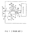
- An example of a control device of a composition capable of shared use of the above two input methods is shown in FIG.1. This FIG.1 is an electrical circuit diagram showing the input circuit part of the control device. As shown in FIG.1, four
diodes 2, 3, 4 and 5,resistor 6 andphotodiode 7a of photocoupler 7 are connected to input terminal 1.Photodetector 7b of photocoupler 7 is connected between a, for example, 5V DC voltage terminal Vp5 and earth. Moreover, the junction point betweenphotodectector 7b and DC voltage terminal Vp5 is connected toinput terminal 8a of microcomputer 8. -
Contacts diodes 2, 3, 4, 5 and a, for example, 24V DC voltage terminal Vp. Also,contacts 12a and 12b, which may be closed by jumper line 11, are provided between the cathode ofdiode 5 ofdiodes 2, 3, 4, 5 and earth. - In the above composition, in the case of allowing sink input to be inputted at input terminal 1,
contacts common earth terminal 13. On the other hand, in the case of allowing source input to be inputted at terminal 1,contacts 12a and 12b are closed by soldering jumper line 11 between them, and contacts SB for source input are connected between a, for example, 24V DC input terminal Vi and input terminal 1. By this means the above input circuit has a shared use composition for the two input methods. - However, with the above prior art composition, four diodes 2 ~ 5 and photocoupler 7 must be added for one input terminal 1. This has the disadvantage of increasing production costs. In particular, many control devices are normally provided with about 10 ~ 100 input terminals. In such cases there was a risk that as many circuit compositions made up of diodes 2 ~ 5 and photocouplers 7 as there were input terminals would have to be provided, and the production costs would increase considerably.
- Accordingly, one object of the present invention is to provide an interface circuit that, while having a composition able to cope with either sink input or source input, may reduce production costs.
- To achieve the above object, in a circuit provided with an input terminal that deals with contact inputs and input signals such as logic, the interface circuit of the present invention provides
- a means of switching that switches between a state in which a pull-up resistor is connected to the above-mentioned input terminal and a state in which a pull-down resistor is connected;
- a means of discrimination that discriminates whether there is sink input or source input by discriminating the switch connection state of this means of switching; and a means of signal switching that switches between a signal output state that outputs an inverted signal of the above-mentioned input signal and a signal output state that outputs the said input signal as it stands, based on the discrimination result of this means of discrimination.
-
- In the above composition, in the case of allowing sink input at the input terminal, the connection state in which the pull-up resistor is connected to the input terminal is produced by the means of switching. On the other hand, in the case of allowing source input at the input terminal, the connection state in which the pull-down resistor is connected to the input terminal is produced by the means of switching. Also, in the case of this composition, discrimination whether it is sink input or source input is performed by the above means of discrimination by discriminating the switch connection state of the above switching means. At the same time, the signal output state is switched by the means of signal switching between a signal output state that outputs an inverted signal of the input signal and a signal output state that outputs the input signal as it stands, based on the above discrimination result.
- By this means, this becomes a composition that may deal with either sink input or source input. Moreover, the means of switching may be achieved by a low-cost composition such as a changeover switch. Also, the means of discrimination may be achieved by a low-cost composition such as a circuit that detects whether the voltage level of the terminal is high level or low level. Furthermore, the means of signal switching, too, may be achieved by such as a simple hardware circuit made up of a logic circuit and a changeover switch, or a microcomputer control function (software). Thus, overall production costs may be reduced.
- Also, in the case of the above composition, a voltage detection circuit is provided that detects the voltage of the levels corresponding to the switch connection states of the above-mentioned means of switching. It is desirable that the above-mentioned means of discrimination should be so composed that it discriminates the switch connection state of the switching circuit, based on the voltage detected by the above-mentioned voltage detection circuit. Moreover, the means of switching may be composed by a manually-operated switch. Furthermore, it is desirable that the means of switching should be composed from a terminal block having a plural of pin terminals and connectors fitted on the pin terminals that short between specified pin terminals. Also, the above-mentioned means of switching may be composed from a plural of lands provided on a printed circuit board and jumper lines that are soldered to these lands and short between specified lands.
- On the other hand, an even more desirable composition is to compose the above-mentioned means of switching from switching elements made up of relays or transistors and a means of switching control that exercises switching control of the above-mentioned switching elements based on external commands. Also, a desirable composition is one composed to provide a means of output switching that switches between an output method that outputs output signals by sink output and an output method that outputs signals by source output, based on the discrimination result of the above-mentioned means of discrimination.
- Moreover, the device may be composed to provide a means of storage that stores the discrimination result discriminated by the above-mentioned means of discrimination at the previous time of operation, and a means of comparison that compares the discrimination result stored by this means of storage and the discrimination result discriminated by the above-mentioned means of discrimination at the current time of operation. In the case of this composition, an even more desirable composition is to provide a means of information that informs of the difference when the discrimination result by the means of discrimination at the previous time of operation and the discrimination result at the current time of operation are judged to differ.
- Also, in the case of the above composition, it is also a good composition to provide a means of self-diagnosis that performs self-diagnosis of the operation of the interface circuit by making and breaking the above-mentioned switching elements in a state in which the above-mentioned input terminal is open and, at the same time judging whether the signals supplied from the above-mentioned switching elements are inverted or not.
- Moreover, in a circuit provided with an input terminal that deals with contact inputs and input signals such as logic, another interface circuit of the present invention provides
- a switching circuit that switches between a connection state in which a pull-up resistor is connected to the above-mentioned input terminal and a connection state in which a pull-down resistor is connected;
- a voltage detection circuit that detects the voltage of the level corresponding to the switch connection state of this switching circuit;
- a discrimination circuit that discriminates whether it is sink input or source input by discriminating the switch connection state of the above-mentioned switching circuit, based on the voltage detected by this detection circuit; and
- a signal switching circuit that switches between a signal output state that outputs a signal that is an inverted signal of the above-mentioned input signal and a signal output state that outputs the said input signal as it stands, based on the discrimination result of this discrimination circuit.
-
- A more complete appreciation of the present invention and many of the attendant advantages thereof will be readily obtained as the same becomes better understood by reference to the following detailed description when considered in connection with the accompanying drawings, wherein:
- FIG.1 is a drawing showing the composition of a prior art interface circuit;
- FIG.2 is an electrical circuit diagram of an input circuit and its environs showing a first embodiment of the present invention;
- FIG.3 is an electrical circuit diagram of a voltage level conversion circuit;
- FIG.4 is an electrical circuit diagram of a voltage level conversion circuit;
- FIG.5 is a time chart;
- FIG.6 is a drawing equivalent to FIG.2 showing a composition that provides three input terminals;
- FIG.7 is a drawing equivalent to FIG.2 showing a second embodiment of the present invention;
- FIG.8 is a drawing equivalent to FIG.2 showing a third embodiment of the present invention;
- FIG.9 is a drawing equivalent to FIG.2 showing a fourth embodiment of the present invention;
- FIG.10 is an electrical circuit diagram of an output circuit and its environs showing a fifth embodiment of the present invention;
- FIG.11 is a drawing equivalent to FIG.10 showing a sixth embodiment of this invention.
-
- Referring now to the drawings, wherein like reference numerals designate identical or corresponding parts throughout the several views, and more particularly to FIG.2 thereof, one embodiment of the present invention will be described.
- Firstly, FIG.2 is an electrical circuit diagram showing the input circuit and environs of
control device 21. As shown in FIG.2,input terminal 22 is connected to common contact c ofchangeover switch 24 viaresistor 23 for pull-up or pull-down use, while at the same time, it is connected to input terminal 26a ofmicrocomputer 26 via voltagelevel conversion circuit 25. - One contact a of the
above changeover switch 24 is connected to, for example, 24V DC voltage terminal Vp, while the other contact b is connected to earth (0V). Thischangeover switch 24 composes the means of switching of the present invention. In this embodiment it is composed by a manually-operated switch (such as, for example, a dip-switch). Also, common contact c ofchangeover switch 24 is connected to input terminal 26b ofmicrocomputer 26 via voltagelevel conversion circuit 27. - In this case, voltage
level conversion circuit 27 is a circuit that converts the voltage level of common contact c ofchangeover switch 24 to a voltage level capable of input bymicrocomputer 26. In practice, when contacts (c - a) ofchangeover switch 24 have been made, it is a circuit that converts the 24V voltage impressed on common contact c to a voltage of, for example, 5V. As shown in Fig.3, the above voltagelevel conversion circuit 27 is composed of, for example,resistor 28 anddiode 29. The cathode ofdiode 29 is connected to 5V DC voltage terminal Vp5. Also, the anode of diode 29 (the terminal to the right ofresistor 28 in FIG.3) is connected to input terminal 26b ofmicrocomputer 26. - Also,
microcomputer 26 is composed to be capable of discriminating the switch connection state ofchangeover switch 24 by detecting the voltage level of common contact c ofchangeover switch 24. In practice,microcomputer 26 is composed to discriminate that contacts (c - a) ofchangeover switch 24 have been made when the voltage inputted atinput terminal 26b is 5V, and to discriminate that contacts (c - b) ofchangeover switch 24 have been made when the voltage inputted atterminal 26b is 0V. In this case,microcomputer 26 has the function of the means of discrimination of the present invention. - Also, if changeover switch 24 is manually operated so that contacts (c - a) of
changeover switch 24 become made,resistor 23 becomes in the connection state of being connected to input terminal 22 as a pull-up resistor, and input by the sink input method becomes possible forinput terminal 22. Here, as shown by the broken line in FIG.2. contacts SA for sink input are connected betweeninput terminal 22 andcommon earth terminal 30. Input signal Si inputted atinput terminal 22 becomes the signal shown in FIG.5(a) when contacts SA are made and broken. - On the other hand, if changeover switch 24 is manually operated so that contacts (c - b) of
changeover switch 24 become made,resistor 23 becomes in the connection state of being connected to input terminal 22 as a pull-down resistor, and input by the source input method becomes possible atinput terminal 22. Here, as shown by the broken lines in FIG.2, contacts SB for source input are connected between, for example, 24V DC voltage terminal Vi andinput terminal 22. Input signal Si inputted atinput terminal 22 becomes the signal shown in FIG.5(b) when contacts SB are made and broken. Here it may be seen that input signal Si for source input has become the inverted signal of input signal Si for sink input (see Fig.5(a)). - Voltage
level conversion circuit 25 is a circuit that converts the voltage level of input signal Si inputted atinput terminal 22 to a voltage level capable of being inputted bymicrocomputer 26. In practice, it is a circuit that converts the 24V voltage Vi impressed oninput terminal 22 to a voltage of, for example, 5V when input signal Si is high level. As shown in FIG.4, voltagelevel conversion circuit 25 is composed fromresistors NPN type transistor 34.Resistor 32, which is connected to the collector oftransistor 34, is connected to 5V DC voltage terminal Vp5. Also, the collector oftransistor 34 is connected to input terminal 26a ofmicrocomputer 26. - Here,
microcomputer 26 is composed to use, as an input signal applied to input terminal 26a, either an inverted input signal (that is to say, input signal Si), or a signal as it was outputted, as logic signal Sa in signal processing withinmicrocomputer 26, depending on the switch connection state ofchangeover switch 24 discriminated in the above-mentioned manner. In practice,microcomputer 26 is composed as follows. It will take the inverted signal of the input signal applied to input terminal 26a (that is to say, input signal Si) as logic signal Sa when it is discriminated that contacts (c - a) ofchangeover switch 24 have been made. On the other hand, it will take the input signal applied to input terminal 26a (that is to say, input signal Si) in the signal state in which it was outputted as logic signal Sa when it is discriminated that contacts (c - b) ofchangeover switch 24 have been made. - By this means, logic signal Sa, used as the input signal within
microcomputer 26, becomes a signal such as shown in FIG.5(c), and it becomes the same signal whether the signal inputted atinput terminal 22 be sink input or source input. That is to say, the above input circuit is of a composition to enable shared use in a 2-input method. In this case,microcomputer 26 functions as the means of signal switching of the present invention. - Also, for example,
non-volatile memory 35 is connected tomicrocomputer 26 as the means of storage.Microcomputer 26 is composed to store the result of the discrimination performed in the above manner, that is to say whether it is sink input or source input, innon-volatile memory 35. Moreover,microcomputer 26 is composed both to read out the discrimination result discriminated at the time of previous operation, which is stored innon-volatile memory 35, and to compare that with the discrimination result at the current time of operation discriminated in the manner described above. In this case,microcomputer 26 functions as the means of comparison of the present invention. -
Microcomputer 26 is so composed that, when it has judged by the above comparison process that the discrimination result of the previous time of operation and the discrimination result of the current time of operation differ, it informs of that difference. For example, it may display that information on a display device (not illustrated) provided on an operating panel. In the case of this composition, the means of information of the present invention is composed bymicrocomputer 26 and the display device. Thus, the user may accurately check that the input method has changed between the previous time of operation and the current time of operation. Therefore, in the unlikely case of the setting of the input method being erroneous, that fact may readily be checked and thus the utmost may be done to prevent the occurrence of incorrect operation. - When using this embodiment composed as above, in the case of sink input being inputted at
input terminal 22, contacts (c - a) are made by the manual operation ofchangeover switch 24, and pull-upresistor 23 is put into the connection state of being connected to input terminal 22. Therefore it is made possible to execute sink input. On the other hand, in the case of source input being inputted, contacts (c - b) are made by the manual operation ofchangeover switch 24, and pull-down resistor 23 is put into the connection state of being connected to input terminal 22. Therefore, the execution of source input is enabled. - Also, in the case of this embodiment, judgement is made as to whether it is sink input or source input through the discrimination of the switching state of
changeover switch 24 bymicrocomputer 26. At the same time, the composition is designed to switch between a signal output state that outputs the inverted signal of input signal Si as logic signal Sa, and a signal output state that outputs input signal Si as it stands as logic signal Sa, based on the result of the above discrimination bymicrocomputer 26. By this means, the input circuit of the above embodiment has a composition capable of response to either sink input or source input. - Moreover, in the case of the above embodiment,
changeover switch 24 is a low-cost composition as the means of switching. Also, the means of judgement is a circuit that detects whether the voltage level of a terminal (in practice, common contact c of changeover switch 24) is high level or low level. In the above embodiment this is achieved by voltagelevel conversion circuit 27 of simple composition and a control function (software) ofmicrocomputer 26. That is to say, the means of judgement may be achieved by a low-cost composition. Furthermore, the means of signal switching is achieved by a control function (software) ofmicrocomputer 26, and is therefore of low-cost composition. Consequently, the input circuit of the above embodiment may reduce production costs in comparison with the prior art composition (see FIG.1). - In particular, with the composition of the above embodiment, in the case of being composed to provide a number of
input terminals 22, production cost may be greatly reduced in comparison with the prior art composition. As a practical illustration of this, a composition that provides threeinput terminals 22 is shown in FIG.6. As shown in FIG.6, even though three input terminals are provided, the composition manages with the provision of only one each ofchangeover switch 24 and voltagelevel conversion circuit 27. Also, although the number of means of signal switching required is the same as the number of input terminals, these are achieved by control functions (software) ofmicrocomputer 26. Thus, a low-cost composition may be achieved. The number ofresistors 23 for pull-up or pull-down use and the number voltagelevel conversion circuits 25 are respectively increased to equal the number (three) of input terminals. However, in both sink input-dedicated input circuits and source input-dedicated input circuits, these parts are parts which must of necessity be increased in number when a number of input terminals are provided. Consequently, when using this embodiment, even when a number of input terminals are provided, it is possible to reduce production costs. - As opposed to this, in the prior art composition (see FIG.1) if a number of input terminals are provided, a circuit composed of four diodes and a photocoupler must be provided for each separate input terminal. Consequently, with the prior art composition, if a number of input terminals are provided, the production cost greatly increases. Thus, the greater the number of input terminals provided, the greater becomes the difference in production costs between the above embodiment and the prior art composition.
- With the above embodiment, voltage
level conversion circuit 27 has been composed as the circuit shown in FIG.3. However, the present invention is not limited to this, and other circuit compositions may be used, provided they are circuits that may convert voltage level. Also, voltagelevel conversion circuit 25 has been composed as the circuit shown in FIG.4. However, the present invention is not limited to this, and other circuit compositions (a circuit composed to use, for example, a photocoupler instead of the transistor) may be used, provided they are circuits that may convert voltage level. - Moreover, if
input terminals microcomputer 26 are composed to be capable of directly inputting voltages of 24V, voltagelevel conversion circuits non-volatile memory 35 is provided as the storage means. However, the present invention is not limited to this, and a composition such as the installation of, for example, a memory (RAM) provided with a battery backup function may be used. - Also, with the above embodiment, the means of signal switching is composed by a control function of
microcomputer 26. However, instead of this the composition may be with a simple hardware circuit made up of a logic circuit and a changeover switch. In practice, as in a second embodiment shown in FIG.7, it is desirable thatsignal switching circuit 36 be composed ofinverter device 37 andchangeover switch 38. In the case of this composition, the composition is to drive the switching ofchangeover switch 38 bymicrocomputer 26, while common contact c ofchangeover switch 38 is connected to input terminal 26a ofmicrocomputer 26.Changeover switch 38 may be composed of, for example, the switching element of a transistor (semiconductor switch). Also, the output terminal of voltagelevel conversion circuit 25 is connected toinverter device 37 and one terminal b ofchangeover switch 38. Moreover,inverter device 37 is connected to the other terminal a ofchangeover switch 38. - In the case of the above composition, when
microcomputer 26 makes contacts (c - a) ofchangeover switch 24 based on the voltage level of common contact c ofchangeover switch 24, that is to say in the case of sink input being discriminated, the composition operateschangeover switch 38 so that its contacts (c - a) become made. On the other hand, whenmicrocomputer 26 makes contacts (c - b), that is to say in the case of source input being discriminated, the composition operateschangeover switch 38 so that its contacts (c - b) become made. - Apart from the above, the composition of the second embodiment is the same as the composition of the first embodiment. Consequently, the second embodiment may also obtain the same operational results as the first embodiment.
- FIG.8 shows a third embodiment of the present invention. It illustrates the places of difference from the first embodiment. Like reference numerals are assigned to parts that are the same as in the first embodiment. In the third embodiment, the means of switching is composed of a terminal block having a plural of pin terminals, and connectors that are fitted on the pin terminals and short between specified pin terminals.
- In practice, as shown in FIG.8, terminal 39, which is connected to DC voltage terminal Vp, terminal 40, which is connected to earth, and terminal 41, which is connected to
resistor 23 and voltagelevel conversion circuit 27, are provided as pin terminals on the terminal block (not illustrated) of (the control device) of an inverter device. Also provided areconnectors - With this composition, in the case of executing sink input, it is composed to short between
terminal 39 and terminal 40 usingconnector 42, by fittingconnector 42 onterminal 39 andterminal 40. On the other hand, in the case of executing source input, it is composed to short betweenterminal 40 and terminal 41 usingconnector 43, by fittingconnector 43 onterminal 40 andterminal 41. -
Microcomputer 26 is composed to discriminate whether there is shorting betweenterminal 39 and terminal 40 (that is to say whether it is sink input) or whether there is shorting betweenterminal 40 and terminal 41 (that is to say whether it is source input) by detecting the voltage level ofterminal 41 via voltagelevel conversion circuit 27. Apart from the above, the composition of the third embodiment is the same as that of the first embodiment. Consequently, the third embodiment may also obtain virtually the same operational results as the first embodiment. - Also, in the third embodiment the means of switching is composed by a plural of pin terminals and connectors. However, instead of this, it may be composed by a plural of lands provided on a printed circuit board and inserting and soldering jumper lines that short between specified lands in pin insertion holes formed in these lands. In the case of this type of composition also, virtually the same operational results may be obtained as with the third embodiment.
- FIG.9 shows a fourth embodiment of the present invention. It illustrates the places of difference from the first embodiment. Like reference numerals are assigned to parts that are the same as in the first embodiment. In the fourth embodiment, the means of switching is composed by a switching device made up of components such as relays or transistors. At the same time, the composition provides a means of switching control that controls the switching of the switching device based on external commands.
- In practice, as shown in FIG.9, the means of switching is composed of
relay 44, which is made up ofcontacts relay coil 44c. In this case,contacts 44a of one relay are connected between DC voltage terminal Vp andresistor 23, andcontacts 44b of the other relay are connected betweenresistor 23 and earth. Also, the composition is such thatrelay coil 44c is controlled bymicrocomputer 45 viadriver circuit 46 to pass/not to pass current. The composition is such that external commands (that is to say commands that set sink input or source input) may be applied tomicrocomputer 45. - Here, as methods of applying external commands to
microcomputer 45, there are such methods as the method of applying commands (for example, parameters) tomicrocomputer 45 based on the operation of various keys provided on an operator panel and the method of sending commands tomicrocomputer 45 via a transmission line from an external terminal, such as a personal computer. - In the case of the above composition, when an external command is applied to
microcomputer 45,microcomputer 45 drives and controls relay 44 based on that command. In practice, in the case of the command being the setting of sink output,microcomputer 45 makesrelay contacts 44a (and also breaksrelay contacts 44b) by makingrelay coil 44c conductive. In the case of the command being, on the contrary, the setting of source input,microcomputer 45 makesrelay contacts 44b (and also breaksrelay contacts 44a) by makingrelay coil 44c non-conductive. At the same time,microcomputer 45 is composed to store the above inputted commands innon-volatile memory 35. - Apart from the above, the composition of the fourth embodiment is the same as that of the first embodiment. Consequently, the fourth embodiment may also obtain virtually the same operational results as the first embodiment. In particular, with the above fourth embodiment, the execution of switching to sink input or source input using external commands is simple.
- Also, with the above fourth embodiment, self-diagnosis of the interface circuit (the input circuit) is possible in the following manner. With
input terminal 22 in the open state,relay contacts relay coil 44c using microcomputer 45. Then, whether the signal applied frominput terminal 22, that is to say the signal outputted from voltagelevel conversion circuit 25, is inverted or not is judged at thistime using microcomputer 45. - In the case of this composition, when it is detected that the signal outputted from voltage
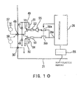
level conversion circuit 25 is inverted, it may be decided that the operations of voltagelevel conversion circuit 25 andrelay 44 of the input circuit are normal. On the other hand, when it is detected that the signal outputted from voltagelevel conversion circuit 25 is not inverted, it may be decided that the operation of one or other of voltagelevel conversion circuit 25 andrelay 44 of the input circuit is abnormal. That is to say, with the above composition,microcomputer 45 composes the means of self-diagnosis of the present invention. - FIG.10 shows a fifth embodiment of the present invention. It illustrates the places of difference from the first embodiment. Like reference numerals are assigned to parts that are the same as in the first embodiment. The fifth embodiment is composed automatically to switch between an output method that outputs an output signal using sink output and an output method that outputs using source output, based on the discrimination result of whether it is sink input or source input.
- The following is a practical description following FIG.10. FIG.10 is an electrical circuit diagram showing an output circuit and its environs. In FIG.10, diodes 47 and 48,
PNP type transistor 49,NPN type transistor 50 andresistors 51 ~ 54 are connected tooutput terminal 46 as shown in the drawing. Also, the base oftransistor 49 is connected tofirst switch 56a viaresistor 52 andinverter device 55. The base oftransistor 50 is connected tosecond switch 56b viaresistor 53. Moreover,first switch 56a andsecond switch 56b are connected tooutput terminal 26e ofmicrocomputer 26. - Also,
microcomputer 26 is composed so that it controls the ON/OFF switching offirst switch 56a andsecond switch 56b. In this case,microcomputer 26 breaksfirst switch 56a and makessecond switch 56b when it has discriminated, in the above-mentioned manner, that there is a sink input. By this means, it becomes possible to output fromoutput terminal 46 by the sink output method. In this case, the composition is such that the load, which is forexample relay coil 57, is connected between DC voltage terminal Vi andoutput terminal 46. - On the other hand,
microcomputer 26 makesfirst switch 56a and breakssecond switch 56b when it has discriminated, in the above-mentioned manner, that there is a source input. By this means, it becomes possible to output fromoutput terminal 46 by the source output method. In this case, the composition is such that the load, which is forexample relay coil 58, is connected betweenoutput terminal 46 andcommon earth terminal 30. In the case of this composition, the means of output method switching of the present invention is composed byfirst switch 56a,second switch 56b andmicrocomputer 26. - Apart from the above, the composition of the fifth embodiment (the composition of the input circuit, and the like) is the same as that of the first embodiment. Consequently, the fifth embodiment may also obtain virtually the same operational results as the first embodiment. In particular, with the above fifth embodiment, whether it is sink input or source input is discriminated by
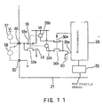
microcomputer 26. At the same time, the composition is such that it performs sink output when the discrimination result is sink input and the composition is also such that it performs source output when the discrimination result is source input. By this means, while it is a composition that is capable of switching input methods, it may also cause the output method to correspond to the input method that has been switched. - FIG.11 shows a sixth embodiment of the present invention. It illustrates the places of difference from the first embodiment. Like reference numerals are assigned to parts that are the same as in the first embodiment. The sixth embodiment is a composition that automatically switches between an output method that outputs the output signal using the sink method and an output method that outputs the output signal using the source method, based on the discrimination result of whether it is sink input or source input. It may achieve this with an electrical circuit composition that differs from the above fifth embodiment.
- In practice, as shown in FIG.11,
relay contacts 58a ofrelay 58 are connected betweenoutput terminal 46 and DC voltage terminal Vp, whilerelay contacts 59a ofrelay 59 are connected between output terminal and earth. Also, a series circuit made up ofrelay coil 58b ofrelay 58 andfirst switch 56a and a series circuit made up ofrelay coil 59b ofrelay 59 andsecond switch 56b are connected in parallel between DC voltage terminal Vp and the collector ofNPN type transistor 60. Moreover, the emitter oftransistor 60 is earthed, while the base is connected tooutput terminal 26e ofmicrocomputer 26. - In the case of the sixth embodiment,
microcomputer 26 breaksfirst switch 56a and makessecond switch 56b when it has discriminated, in the above-mentioned manner, that it is a sink input. By this means, it becomes possible to output fromoutput terminal 46 by the sink output method. In this case, the load, which is forexample relay coil 57, is connected between DC voltage terminal Vi andoutput terminal 46. - On the other hand,
microcomputer 26 makesfirst switch 56a and breakssecond switch 56b when it has discriminated, in the above mentioned manner, that there is a source input. By this means, it becomes possible to output fromoutput terminal 46 by the source output method. In this case, the load, which is forexample relay coil 58, is connected betweenoutput terminal 46 andcommon earth terminal 30. Apart from the above, the composition of the sixth embodiment is the same as that of the fifth embodiment. Consequently, the sixth embodiment may also obtain virtually the same operational results as the fifth embodiment. - In the above various embodiments, the interface circuit of the present invention has been applied to the input circuits of control devices for inverter devices. However, it is not limited to this and it may be applied to the input circuits of other control devices.
- As will be clear from the above description, the present invention is composed to provide:
- a means of switching that switches between a connection state in which a pull-up resistor is connected to the input terminal and a connection state in which a pull-down resistor is connected to the input terminal;
- a means of discrimination that discriminates whether it is sink input or source input by discriminating the switch connection state of this means of switching; and
- a means of signal switching that switches between a signal output state that outputs a signal that is an inversion of the said input signal and a signal output state that outputs the said input signal as it stands, based on the discrimination result of this discrimination means.
-
- Thus it is a composition that may respond to either sink input or source input. Therefore, it will achieve the excellent effect of being able to reduce production costs.
- Obviously, numerous modifications and variations of the present invention are possible in the light of the above teachings. It is therefore to be understood that within the scope of the appended claims, the present invention may be practiced otherwise than as specially described herein.
Claims (11)
- An interface circuit provided with a terminal that deals with contact inputs and input signals such as logic, comprising:a means of switching that switches between a connection state in which a pull-up resistor is connected to said input terminal and a connection state in which a pull-down resistor is connected to said input terminal;a means of discrimination that discriminates whether it is sink input or source input by discriminating the switch connection state of means of switching; anda means of signal switching that switches between a signal output state that outputs a signal that is an inversion of said input signal and a signal output state that outputs said input signal as it stands, based on the discrimination result of said means of discrimination.
- An interface circuit according to Claim 1, and further comprising:a voltage detection circuit that detects the voltage of the level that corresponds to the switch connection state of the said means of switching;wherein said means of discrimination is composed to discriminate the switch connection state of said switching circuit, based on the voltage detected by said voltage detection circuit.
- An interface circuit according to Claims 1 or 2, wherein:
said means of switching is composed of a manual switch. - An interface circuit according to Claims 1 or 2, wherein:
said means of switching is composed of a terminal block having a plural of pin terminals, and connectors that are fitted to said pin terminals and make connection between specified pin terminals. - An interface circuit according to Claims 1 or 2, wherein:
said means of switching is composed of a plural of lands provided on a printed circuit board, and jumper lines that are soldered to said lands and make connection between specified lands. - An interface circuit according to Claims 1 or 2, wherein:
said means of switching is composed of switching devices made up of relays or transistors, and a means of switching control that controls the switching of said switching devices, based on external commands. - An interface circuit according to any of Claims 1 to 6, and further comprising:
a means of output method switching that switches between an output method that outputs output signals using sink output and an output method that outputs output signals using source output, based on the discrimination result of said means of discrimination. - An interface circuit according to any of Claims 1 to 7, and further comprising:a means of storage that stores the discrimination result discriminated by said means of discrimination at the previous time of operation; anda means of comparison that compares said stored discrimination result with said discrimination result discriminated by said means of discrimination at the current time of operation.
- An interface circuit according to Claim 8,and further comprising:
a means of information that informs of that difference when it is judged by said means of comparison that said discrimination result of the previous time of operation and said discrimination result of the current time of operation differ. - An interface circuit according to Claim 6, and further comprising:
a means of self-diagnosis that performs self-diagnosis of the operation of said interface circuit, by making and breaking said switching devices in a state in which said input terminal is open and, at the same time, judging whether or not the signal supplied from said input terminal is inverted. - An interface circuit provided with a terminal that deals with contact inputs and input signals such as logic, comprising:a switching circuit that switches between a connection state in which a pull-up resistor is connected to said input terminal and a connection state in which a pull-down resistor is connected to said input terminal;a voltage detection circuit that detects voltages of levels corresponding to switch connection states of said switching circuit;a discrimination circuit that discriminates whether it is sink input or source input by discriminating said switch connection state of said switching circuit, based on the voltage detected by said voltage detection circuit; anda signal switching circuit that switches between a signal output state that outputs a signal that is an inversion of said input signal and a signal output state that outputs said input signal as it stands, based on the discrimination result of said discrimination circuit.
Applications Claiming Priority (3)
| Application Number | Priority Date | Filing Date | Title |
|---|---|---|---|
| JP32437097A JP3557335B2 (en) | 1997-11-26 | 1997-11-26 | Interface circuit |
| JP32437097 | 1997-11-26 | ||
| JP324370/97 | 1997-11-26 |
Publications (3)
| Publication Number | Publication Date |
|---|---|
| EP0920134A2 true EP0920134A2 (en) | 1999-06-02 |
| EP0920134A3 EP0920134A3 (en) | 2000-11-08 |
| EP0920134B1 EP0920134B1 (en) | 2008-04-02 |
Family
ID=18165038
Family Applications (1)
| Application Number | Title | Priority Date | Filing Date |
|---|---|---|---|
| EP98309680A Expired - Lifetime EP0920134B1 (en) | 1997-11-26 | 1998-11-25 | Interface circuit |
Country Status (4)
| Country | Link |
|---|---|
| US (1) | US6181189B1 (en) |
| EP (1) | EP0920134B1 (en) |
| JP (1) | JP3557335B2 (en) |
| DE (1) | DE69839322T2 (en) |
Cited By (1)
| Publication number | Priority date | Publication date | Assignee | Title |
|---|---|---|---|---|
| CN101019093B (en) * | 2005-09-27 | 2010-07-28 | 埃派克森微电子有限公司 | Circuit and process for photo coupling detection |
Families Citing this family (14)
| Publication number | Priority date | Publication date | Assignee | Title |
|---|---|---|---|---|
| US6429680B1 (en) * | 2000-11-01 | 2002-08-06 | Semiconductor Components Industries Llc | Pin programmable reference |
| JP4536274B2 (en) * | 2001-02-02 | 2010-09-01 | サンクス株式会社 | Signal input circuit |
| JP4524661B2 (en) * | 2005-10-06 | 2010-08-18 | 株式会社デンソー | Power generation control device |
| JP4948228B2 (en) * | 2007-03-29 | 2012-06-06 | 株式会社クボタ | Work machine interface circuit |
| JP5173317B2 (en) * | 2007-08-23 | 2013-04-03 | 東芝シュネデール・インバータ株式会社 | Inverter device |
| US7528399B1 (en) * | 2008-01-21 | 2009-05-05 | Delta Electronics, Inc. | Controlling apparatus for gate driving signal |
| JP2009194956A (en) * | 2008-02-12 | 2009-08-27 | Toshiba Schneider Inverter Corp | Inverter device |
| JP5507973B2 (en) * | 2009-11-17 | 2014-05-28 | 東芝シュネデール・インバータ株式会社 | Inverter device and control device |
| WO2012025996A1 (en) * | 2010-08-24 | 2012-03-01 | 三菱電機株式会社 | Power conversion device |
| JP2017228204A (en) * | 2016-06-24 | 2017-12-28 | 株式会社ノーリツ | Control circuit |
| JP7068220B2 (en) | 2019-03-18 | 2022-05-16 | ファナック株式会社 | Digital signal output device that outputs digital signals according to the operation switch |
| CN110061732B (en) * | 2019-04-25 | 2023-05-26 | 东莞铭普光磁股份有限公司 | Level conversion circuit and level conversion method supporting SPI communication |
| JP2022083899A (en) * | 2020-11-25 | 2022-06-06 | 富士電機株式会社 | Driving device |
| CN116346117B (en) * | 2022-12-19 | 2024-01-19 | 深圳市芊熠智能硬件有限公司 | IIC port expansion circuit, transmission method, transmission system, computer equipment and medium |
Citations (2)
| Publication number | Priority date | Publication date | Assignee | Title |
|---|---|---|---|---|
| US5414305A (en) * | 1992-10-13 | 1995-05-09 | Nakamura; Makoto | Output circuit having capability of keeping logic state of signal sent between logic circuits |
| JPH07254852A (en) * | 1994-03-15 | 1995-10-03 | Omron Corp | Multi-input circuit, circuit and controller using the same circuit |
Family Cites Families (4)
| Publication number | Priority date | Publication date | Assignee | Title |
|---|---|---|---|---|
| US4763023A (en) * | 1987-02-17 | 1988-08-09 | Rockwell International Corporation | Clocked CMOS bus precharge circuit having level sensing |
| US5117123A (en) * | 1990-04-30 | 1992-05-26 | Thomson Consumer Electronics, Inc. | Diode switch providing temperature compensated d.c. bias for cascaded amplifier |
| US5257223A (en) * | 1991-11-13 | 1993-10-26 | Hewlett-Packard Company | Flip-flop circuit with controllable copying between slave and scan latches |
| US5583452A (en) * | 1995-10-26 | 1996-12-10 | Xilinx, Inc. | Tri-directional buffer |
-
1997
- 1997-11-26 JP JP32437097A patent/JP3557335B2/en not_active Expired - Fee Related
-
1998
- 1998-11-25 US US09/199,792 patent/US6181189B1/en not_active Expired - Lifetime
- 1998-11-25 DE DE69839322T patent/DE69839322T2/en not_active Expired - Lifetime
- 1998-11-25 EP EP98309680A patent/EP0920134B1/en not_active Expired - Lifetime
Patent Citations (2)
| Publication number | Priority date | Publication date | Assignee | Title |
|---|---|---|---|---|
| US5414305A (en) * | 1992-10-13 | 1995-05-09 | Nakamura; Makoto | Output circuit having capability of keeping logic state of signal sent between logic circuits |
| JPH07254852A (en) * | 1994-03-15 | 1995-10-03 | Omron Corp | Multi-input circuit, circuit and controller using the same circuit |
Non-Patent Citations (1)
| Title |
|---|
| PATENT ABSTRACTS OF JAPAN vol. 1996, no. 02, 29 February 1996 (1996-02-29) & JP 07 254852 A (OMRON CORP), 3 October 1995 (1995-10-03) * |
Cited By (1)
| Publication number | Priority date | Publication date | Assignee | Title |
|---|---|---|---|---|
| CN101019093B (en) * | 2005-09-27 | 2010-07-28 | 埃派克森微电子有限公司 | Circuit and process for photo coupling detection |
Also Published As
| Publication number | Publication date |
|---|---|
| EP0920134B1 (en) | 2008-04-02 |
| US6181189B1 (en) | 2001-01-30 |
| EP0920134A3 (en) | 2000-11-08 |
| DE69839322T2 (en) | 2009-04-16 |
| JPH11161391A (en) | 1999-06-18 |
| JP3557335B2 (en) | 2004-08-25 |
| DE69839322D1 (en) | 2008-05-15 |
Similar Documents
| Publication | Publication Date | Title |
|---|---|---|
| EP0920134B1 (en) | Interface circuit | |
| US5802328A (en) | Apparatus for detecting correct insertion of a PC card in an information processing system | |
| US5672917A (en) | Semiconductor power switch system | |
| JP3187990B2 (en) | Electronic control unit for switching multiple loads | |
| US6522937B2 (en) | Hand-held device for a programmable control unit | |
| US7913002B2 (en) | Test apparatus, configuration method, and device interface | |
| US8159239B2 (en) | Testing apparatus for testing electronic system with 5-wire resistive touch panel and the method therefor | |
| FI79226B (en) | EN AUDIO / VIDEOADAPTER FOER AUDIOVISUELLA APPARATER. | |
| CN112380066B (en) | Server maintenance and debugging device based on domestic platform and server | |
| EP4206697A1 (en) | Self-locking and detection circuit and apparatus, and control method | |
| US6226602B1 (en) | Electric circuit arrangement | |
| CN113131923A (en) | Source type drain type automatic compatible interface circuit | |
| US6744386B2 (en) | Prevention of incompatible keyboard selections from being entered during power initialization | |
| CN101316045B (en) | Battery charging apparatus used for portable system | |
| CN101464473B (en) | Electric voltage exception protection device used for circuit board test | |
| EP0906886A1 (en) | Control circuit | |
| CN100449635C (en) | Method and system for detecting disk drive state | |
| KR100706845B1 (en) | Auto wiring system | |
| US7173673B2 (en) | Expanded switching of video/S-video signals by auto-sense apparatus designed to initiate switching of a different type of video signal and apparatus for emulating one type of signal by another type of signal to initiate said switching | |
| GB2306089A (en) | BNC/D-Sub signal auto-selection circuit | |
| CN100428602C (en) | Control circuit of electric power supplier with fixed current limiting mode | |
| JPH08234878A (en) | Device with interface selecting function | |
| MXPA96005930A (en) | Circuit of switching of signal of entrance of a monitor and method of switching of mi | |
| KR100717053B1 (en) | Method for detecting plug type inserted into common jack and apparatus therefore | |
| CN117269845A (en) | Method for identifying and displaying line faults and measuring meter |
Legal Events
| Date | Code | Title | Description |
|---|---|---|---|
| PUAI | Public reference made under article 153(3) epc to a published international application that has entered the european phase |
Free format text: ORIGINAL CODE: 0009012 |
|
| 17P | Request for examination filed |
Effective date: 19981222 |
|
| AK | Designated contracting states |
Kind code of ref document: A2 Designated state(s): DE FR GB IT |
|
| AX | Request for extension of the european patent |
Free format text: AL;LT;LV;MK;RO;SI |
|
| PUAL | Search report despatched |
Free format text: ORIGINAL CODE: 0009013 |
|
| AK | Designated contracting states |
Kind code of ref document: A3 Designated state(s): AT BE CH CY DE DK ES FI FR GB GR IE IT LI LU MC NL PT SE |
|
| AX | Request for extension of the european patent |
Free format text: AL;LT;LV;MK;RO;SI |
|
| RIC1 | Information provided on ipc code assigned before grant |
Free format text: 7H 03K 19/173 A, 7H 03K 19/0175 B |
|
| AKX | Designation fees paid |
Free format text: DE FR GB IT |
|
| GRAP | Despatch of communication of intention to grant a patent |
Free format text: ORIGINAL CODE: EPIDOSNIGR1 |
|
| GRAS | Grant fee paid |
Free format text: ORIGINAL CODE: EPIDOSNIGR3 |
|
| GRAA | (expected) grant |
Free format text: ORIGINAL CODE: 0009210 |
|
| AK | Designated contracting states |
Kind code of ref document: B1 Designated state(s): DE FR GB IT |
|
| REG | Reference to a national code |
Ref country code: GB Ref legal event code: FG4D |
|
| REF | Corresponds to: |
Ref document number: 69839322 Country of ref document: DE Date of ref document: 20080515 Kind code of ref document: P |
|
| ET | Fr: translation filed | ||
| PLBE | No opposition filed within time limit |
Free format text: ORIGINAL CODE: 0009261 |
|
| STAA | Information on the status of an ep patent application or granted ep patent |
Free format text: STATUS: NO OPPOSITION FILED WITHIN TIME LIMIT |
|
| 26N | No opposition filed |
Effective date: 20090106 |
|
| PGFP | Annual fee paid to national office [announced via postgrant information from national office to epo] |
Ref country code: IT Payment date: 20101120 Year of fee payment: 13 |
|
| PG25 | Lapsed in a contracting state [announced via postgrant information from national office to epo] |
Ref country code: IT Free format text: LAPSE BECAUSE OF NON-PAYMENT OF DUE FEES Effective date: 20121125 |
|
| PGFP | Annual fee paid to national office [announced via postgrant information from national office to epo] |
Ref country code: DE Payment date: 20141118 Year of fee payment: 17 Ref country code: FR Payment date: 20141110 Year of fee payment: 17 Ref country code: GB Payment date: 20141119 Year of fee payment: 17 |
|
| REG | Reference to a national code |
Ref country code: DE Ref legal event code: R119 Ref document number: 69839322 Country of ref document: DE |
|
| GBPC | Gb: european patent ceased through non-payment of renewal fee |
Effective date: 20151125 |
|
| REG | Reference to a national code |
Ref country code: FR Ref legal event code: ST Effective date: 20160729 |
|
| PG25 | Lapsed in a contracting state [announced via postgrant information from national office to epo] |
Ref country code: GB Free format text: LAPSE BECAUSE OF NON-PAYMENT OF DUE FEES Effective date: 20151125 Ref country code: DE Free format text: LAPSE BECAUSE OF NON-PAYMENT OF DUE FEES Effective date: 20160601 |
|
| PG25 | Lapsed in a contracting state [announced via postgrant information from national office to epo] |
Ref country code: FR Free format text: LAPSE BECAUSE OF NON-PAYMENT OF DUE FEES Effective date: 20151130 |