EP0913764B1 - Method and apparatus for shifting data - Google Patents
Method and apparatus for shifting data Download PDFInfo
- Publication number
- EP0913764B1 EP0913764B1 EP98119827A EP98119827A EP0913764B1 EP 0913764 B1 EP0913764 B1 EP 0913764B1 EP 98119827 A EP98119827 A EP 98119827A EP 98119827 A EP98119827 A EP 98119827A EP 0913764 B1 EP0913764 B1 EP 0913764B1
- Authority
- EP
- European Patent Office
- Prior art keywords
- register
- bits
- output
- bit
- input
- Prior art date
- Legal status (The legal status is an assumption and is not a legal conclusion. Google has not performed a legal analysis and makes no representation as to the accuracy of the status listed.)
- Expired - Lifetime
Links
Images
Classifications
-
- G—PHYSICS
- G06—COMPUTING; CALCULATING OR COUNTING
- G06F—ELECTRIC DIGITAL DATA PROCESSING
- G06F9/00—Arrangements for program control, e.g. control units
- G06F9/06—Arrangements for program control, e.g. control units using stored programs, i.e. using an internal store of processing equipment to receive or retain programs
- G06F9/30—Arrangements for executing machine instructions, e.g. instruction decode
- G06F9/30098—Register arrangements
-
- G—PHYSICS
- G06—COMPUTING; CALCULATING OR COUNTING
- G06F—ELECTRIC DIGITAL DATA PROCESSING
- G06F5/00—Methods or arrangements for data conversion without changing the order or content of the data handled
- G06F5/01—Methods or arrangements for data conversion without changing the order or content of the data handled for shifting, e.g. justifying, scaling, normalising
-
- H—ELECTRICITY
- H03—ELECTRONIC CIRCUITRY
- H03K—PULSE TECHNIQUE
- H03K19/00—Logic circuits, i.e. having at least two inputs acting on one output; Inverting circuits
- H03K19/20—Logic circuits, i.e. having at least two inputs acting on one output; Inverting circuits characterised by logic function, e.g. AND, OR, NOR, NOT circuits
Definitions
- the present invention relates to a method and apparatus for extracting data.
- Such a method and apparatus are usually used in any kind of microprocessors or micro controllers. Internally, data are represented in different registers of the register file of a microprocessor or micro controller.
- a 32-bit microprocessor can have a register file containing, for example, thirty-two 32 bit wide registers. For many purposes, 32 bits are not enough to represent a specific data. Therefore, for example, two registers are concatenated to form a 64-bit register. For processing data having this specific data size of 64 bits, special instructions are provided. One of these instructions is the so-called extracting instruction which provides the ability to extract a certain number of bits out of a data word represented by two or more registers. Such an instruction is, in particular, used to normalize data, for example, the result of a DSP filter accumulation.
- Fig. 1 shows a diagram representing the effect of an extracting instruction.
- Numerals 1 and 2 indicate registers which are concatenated to form a single 64-bit data register. Therefore, each register 1 and 2 has a width of 32 bits.
- the extracting instruction is able to extract 32 bits of the 64-bit word and store it in a register 3 representing the result of the operation.
- the extracting instruction concatenates two data register sources to form a 64-bit value from which 32 consecutive bits are extracted.
- Such an operation can be thought of as a left shift by the number of bits followed by the truncation of the least significant 32 bits of the result.
- the value of the number of bits comes from either a data register or from an immediate data. Therefore, such an instruction usually has up to four parameters indicating the registers containing the 64-bit value, a parameter indicating the value of the position of the extracting word within the 64-bit register, and a register to write the result to.
- such an extracting instruction can be used to normalize the result of a digital signal processor filter accumulation in which a 64-bit accumulator is used for several guard bits.
- the value of the position within the 64-bit accumulator can be determined by using the count leading signs instruction.
- the extracting instruction can also be used to perform a multi-bit rotation by using the same source register for both of the sources that are concatenated.
- U.S. patent 4,495,598 discloses a computer rotate function
- U.S. patent 4,467,444 discloses a processor unit for microcomputer systems which complex three-operand instructions in a single clock cycle.
- U.S. Patent 5,295,250 shows a microprocessor with a barrel shifter.
- the barrel shifter serves as a shift unit which is controlled by a microprogram and operated by micro instructions for performing extraction, insertion and comparison of consecutive bit strings in word data.
- a shifter having the size of the respective register is necessary.
- the word to be extracted starts at bit position 21 and ends at bit position 53.
- a 64-bit shifter would therefore be necessary to shift the content of the 64-bit register 1, 2 by 10 bits to the left and store the result in register 3.
- Fig. 1 of U.S. 5,295,250 shows such an arrangement whereby numeral 104 indicates the barrel shifter.
- a 64-bit shifter requires a large amount of silicon area. It is therefore the object of the present invention to provide a method and apparatus for extracting data as defined in independent claims 1 and 2, respectively, and which simplifies the hardware required to perform such an instruction. This object is achieved for the method by:
- an apparatus for extracting n bits out of a data word stored in two concatenated registers, each having a bit size of n bits starting with the m-th bit of the data register, whereby m being smaller than n comprises:
- the present invention uses the existing resources of the arithmetic logic unit of a microprocessor to perform the above-mentioned extracting instruction without requiring any additional hardware, in particular a 64-bit shifter.
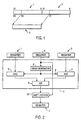
- Fig. 2 shows a block diagram containing those elements which are necessary to perform an extracting instruction.
- Two 32-bit registers 1 and 2 are concatenated and form a 64-bit register.
- Another register 4 is provided which contains a constant indicating the position in between the 64-bit register of the 32-bit data word which is to be extracted. All three registers 1, 2 and 4 are connected to a logical combining circuit 11.
- the logical combining circuit 11 contains a mask generator 6, the input of which is connected to register 4.
- two AND operators 5 and 7 are provided. AND operator 5 has two inputs, the first input is connected to register 1 and the second input is connected to the output of mask generator 6. The second and operator also has two inputs.
- the first input of the end operator 7 is connected to register 2, the second input is connected to the output of an inverter 8 whose input is connected to the output of the mask generator 6.
- an OR operator 9 is provided which comprises two inputs, and one output.
- the first input of OR operator 9 is connected to the output of AND operator 5 and the second input of OR operator 9 is connected to the output of AND operator 7.
- the output of OR operator 9 forms the output of the logical combining circuit 11.
- a shift/rotate register 10 having an input, an output, and a control input is provided.
- This shift/rotate register can be, for example, a barrel shifter.
- the input of shift/rotate register 10 is connected to the output of OR operator 9.
- the control input of shift/rotate register 10 is coupled with the output of register 4.
- a register 3 is provided which is connected to the output of shift/rotate register 10 and contains the result of the extracting operation.
- the extracting instruction may be represented by a mnemonic DEXTR followed by four parameters.
- the first parameter indicates the target register into which the result is written.
- the second and third parameter indicate that two registers which form the 64-bit register.
- the fourth parameter can be a register or a constant indicating the position of the 32-bit word within the 64-bit register.
- Register 4 is supplied to the mask generator 6 which generates a mask containing "003FFFFF". In other words, the first 10 most significant bits are set to zero and the rest of the bits to one.
- This mask is ANDed with the content of register 1 to create "0037A549", while the inverse of the mask, which will be "FFC00000”, is ANDed with the content of register 2 to create "B0800000”.
- These two intermediate results which are accessible at the outputs of the two end operators 5 and 7 are then ORed by the OR operator 9 to create "B0B7A549". This intermediate result which is accessible at the output of OR operator 9 is then fed to the input of shift/rotate register 10.
- the shift/rotate register 10 is controlled by the content of register 4 which indicates in this example that the content of shift/rotate register 10 is to be shifted leftwards 10 times.
- the shift/rotate register operates as a rotate register which rotates the content leftwards a number of times as indicated by the control input.
- the 32-bit rotate register 10 produces the result "DE9526C2", which is stored in register 3.
- this solution uses only a 32-bit shifter and mask generator, the area impact of implementing and extracting instruction is mitigated. Compared to a solution using a 64-bit shifter, this solution, according to the present invention, is consuming at least only half the area of silicon. Since less logic is used, transient power consumption is reduced. Another advantage of the present invention is that a small shifter results in faster execution because fewer levels of multiplexer stages are used to build the barrel shifter.
Landscapes
- Engineering & Computer Science (AREA)
- Theoretical Computer Science (AREA)
- Physics & Mathematics (AREA)
- General Engineering & Computer Science (AREA)
- General Physics & Mathematics (AREA)
- Software Systems (AREA)
- Computer Hardware Design (AREA)
- Computing Systems (AREA)
- Mathematical Physics (AREA)
- Executing Machine-Instructions (AREA)
Description
- The present invention relates to a method and apparatus for extracting data.
- Such a method and apparatus are usually used in any kind of microprocessors or micro controllers. Internally, data are represented in different registers of the register file of a microprocessor or micro controller.
- An example for such method and apparatus is disclosed in D1:
- "MULTIPRECISION BARREL SHIFTER", IBM Technical Disclosure Bulletin, vol 32, No. 9A, ! Febr. 1990, pages 334-337, XP000083097.
-
- A 32-bit microprocessor can have a register file containing, for example, thirty-two 32 bit wide registers. For many purposes, 32 bits are not enough to represent a specific data. Therefore, for example, two registers are concatenated to form a 64-bit register. For processing data having this specific data size of 64 bits, special instructions are provided. One of these instructions is the so-called extracting instruction which provides the ability to extract a certain number of bits out of a data word represented by two or more registers. Such an instruction is, in particular, used to normalize data, for example, the result of a DSP filter accumulation.
- Fig. 1 shows a diagram representing the effect of an extracting instruction.
Numerals register register 3 representing the result of the operation. As mentioned above, the extracting instruction concatenates two data register sources to form a 64-bit value from which 32 consecutive bits are extracted. Such an operation can be thought of as a left shift by the number of bits followed by the truncation of the least significant 32 bits of the result. The value of the number of bits comes from either a data register or from an immediate data. Therefore, such an instruction usually has up to four parameters indicating the registers containing the 64-bit value, a parameter indicating the value of the position of the extracting word within the 64-bit register, and a register to write the result to. - As mentioned before, such an extracting instruction can be used to normalize the result of a digital signal processor filter accumulation in which a 64-bit accumulator is used for several guard bits. The value of the position within the 64-bit accumulator can be determined by using the count leading signs instruction. The extracting instruction can also be used to perform a multi-bit rotation by using the same source register for both of the sources that are concatenated.
- U.S. patent 4,495,598 discloses a computer rotate function and U.S. patent 4,467,444 discloses a processor unit for microcomputer systems which complex three-operand instructions in a single clock cycle.
- U.S. Patent 5,295,250 shows a microprocessor with a barrel shifter. The barrel shifter serves as a shift unit which is controlled by a microprogram and operated by micro instructions for performing extraction, insertion and comparison of consecutive bit strings in word data.
- To perform such an instruction, usually a shifter having the size of the respective register is necessary. In Fig. 1, it is assumed that the word to be extracted starts at
bit position 21 and ends atbit position 53. A 64-bit shifter would therefore be necessary to shift the content of the 64-bit register register 3. Fig. 1 of U.S. 5,295,250 shows such an arrangement whereby numeral 104 indicates the barrel shifter. - A 64-bit shifter requires a large amount of silicon area. It is therefore the object of the present invention to provide a method and apparatus for extracting data as defined in
independent claims - Storing a start location for the extracted n bits in a third register having a bit size of n bits,
- replacing the m significant bits of the first register with the m significant bits of the second register, wherein the m significant bits to replace are controlled by the third register,
- storing the result in a fourth register, and
- rotating the content of said fourth register by m bits, wherein the m bits of rotation are controlled by the third register.
-
- According to another object of the invention an apparatus for extracting n bits out of a data word stored in two concatenated registers, each having a bit size of n bits starting with the m-th bit of the data register, whereby m being smaller than n comprises:
- A first and second register containing the data word,
- a third register indicating the start location of the extracted data,
- a logical combining circuit for replacing the m significant bits of the first register with the m significant bits of the second register having inputs, a control input, and one output, said inputs of said logical combining circuit being connected to said registers and said control input being connected to said third register, and
- a n-bit shift/rotate means having an input and an output and a control input. said input being connected to said output of said logical combining register and said control input being connected to said third register.
-
- The present invention uses the existing resources of the arithmetic logic unit of a microprocessor to perform the above-mentioned extracting instruction without requiring any additional hardware, in particular a 64-bit shifter.
-
- Fig. 1 shows a diagram representing an extracting instruction, and
- Fig. 2 shows a block diagram representing the hardware which is required to perform an extracting instruction according to the present invention.
-
- Fig. 2 shows a block diagram containing those elements which are necessary to perform an extracting instruction. Two 32-
bit registers register 4 is provided which contains a constant indicating the position in between the 64-bit register of the 32-bit data word which is to be extracted. All threeregisters circuit 11. The logical combiningcircuit 11 contains a mask generator 6, the input of which is connected to register 4. Furthermore, two ANDoperators 5 and 7 are provided. AND operator 5 has two inputs, the first input is connected to register 1 and the second input is connected to the output of mask generator 6. The second and operator also has two inputs. The first input of theend operator 7 is connected to register 2, the second input is connected to the output of aninverter 8 whose input is connected to the output of the mask generator 6. Finally, an OR operator 9 is provided which comprises two inputs, and one output. The first input of OR operator 9 is connected to the output of AND operator 5 and the second input of OR operator 9 is connected to the output ofAND operator 7. The output of OR operator 9 forms the output of the logical combiningcircuit 11. A shift/rotate register 10 having an input, an output, and a control input is provided. This shift/rotate register can be, for example, a barrel shifter. The input of shift/rotate register 10 is connected to the output of OR operator 9. The control input of shift/rotate register 10 is coupled with the output ofregister 4. Finally, aregister 3 is provided which is connected to the output of shift/rotateregister 10 and contains the result of the extracting operation. - In this preferred embodiment, the extracting instruction may be represented by a mnemonic DEXTR followed by four parameters. The first parameter indicates the target register into which the result is written. The second and third parameter indicate that two registers which form the 64-bit register. The fourth parameter can be a register or a constant indicating the position of the 32-bit word within the 64-bit register.
- To show the operation of the extracting instruction according to the present invention, it is assumed that the registers have the following content: register 1 = "A537A549"; register 2 = "B0B0B0B0"; register 4 ="0000000A". All contents of the registers are hexadecimal. As each register is 32 bits wide, only the bottom 5 bits of
register 4 are used in this embodiment. Since the shift value inregister 4 is 10, the result which will be written intoregister 3 is equal to 32 bits of the 64 bit register 1 and 2, starting withbit 53 as the most significant bit and ending withbit 21 as the least significant bit. - The following explains the operation of the hardware according to Fig. 2, step-by-step.
Register 4 is supplied to the mask generator 6 which generates a mask containing "003FFFFF". In other words, the first 10 most significant bits are set to zero and the rest of the bits to one. This mask is ANDed with the content ofregister 1 to create "0037A549", while the inverse of the mask, which will be "FFC00000", is ANDed with the content ofregister 2 to create "B0800000". These two intermediate results which are accessible at the outputs of the twoend operators 5 and 7 are then ORed by the OR operator 9 to create "B0B7A549". This intermediate result which is accessible at the output of OR operator 9 is then fed to the input of shift/rotateregister 10. The shift/rotateregister 10 is controlled by the content ofregister 4 which indicates in this example that the content of shift/rotateregister 10 is to be shifted leftwards 10 times. To perform the proper operation, the shift/rotate register operates as a rotate register which rotates the content leftwards a number of times as indicated by the control input. In other words, the 32-bit rotateregister 10 produces the result "DE9526C2", which is stored inregister 3. - Since this solution according to the preferred embodiment uses only a 32-bit shifter and mask generator, the area impact of implementing and extracting instruction is mitigated. Compared to a solution using a 64-bit shifter, this solution, according to the present invention, is consuming at least only half the area of silicon. Since less logic is used, transient power consumption is reduced. Another advantage of the present invention is that a small shifter results in faster execution because fewer levels of multiplexer stages are used to build the barrel shifter.
Claims (3)
- Method for extracting n bits out of a data word stored in two concatenated registers each having a bit size of n bits starting with the m-th bit of the data register, m being smaller than n, comprising the steps of:storing a start location for the extracted n bits in a third register (4) having a bit size of n bits,replacing the m significant bits of the first register (1) with the m significant bits of the second register (2), wherein the m significant bits to replace are controlled by the third register, and wherein replacing the m significant bits includes:generating a mask (6) which comprises m bits of a first kind and m minus n bits of a second kind,combining the mask with the first register with an AND-operation to create a first result (5),combining the inverted mask with the second register with a second AND-operation to create a second result (7), andcombining the first result and the second result by a OR-operation to create a third result (9),rotating the third result by m bits to create a fourth result (10), wherein the m bits of rotation are controlled by the third register, andstoring the fourth result in a fourth register (3).
- Apparatus for extracting n bits out of a data word stored in two concatenated registers each having a bit size of n bits starting with the m-th bit of the data register, m being smaller than n, comprising:A first and second register containing the data word,a third register indicating the start location of the extracted data,a logical combining circuit for replacing the m significant bits of the first register with the m significant bits of the second register, the logical combining circuit including:a mask generator (6) having an input and an output, said input being connected to said third register,a first AND-operator (5) with inputs and an output, said inputs being connected to said first register and said output of said mask generator,a second AND-operator (7) with inputs and an output, one input being connected to said second register and the other input being fed by the inverted output signal of said mask generator (8), andan OR-operator (9) having inputs and an output, said inputs being connected to said outputs of said first and second AND-operators,
anda n-bit shift/rotate means (10) to shift said output of said OR-operator by m bits, said n-bit shift/rotate means having an input and an output and a control input. said input being connected to said output of said OR-operator and said control input being connected to said third register, anda fourth register (3) to store said output of said n-bit shift/ rotate means said fourth register having an input and an output, said input being connected to said output of said n-bit shift/ rotate means. - Apparatus according to claim 2, wherein the boolean operators and the shift/rotate means are part of an arithmetic logic unit of a microprocessor.
Applications Claiming Priority (2)
| Application Number | Priority Date | Filing Date | Title |
|---|---|---|---|
| US961384 | 1997-10-30 | ||
| US08/961,384 US6052522A (en) | 1997-10-30 | 1997-10-30 | Method and apparatus for extracting data stored in concatenated registers |
Publications (2)
| Publication Number | Publication Date |
|---|---|
| EP0913764A1 EP0913764A1 (en) | 1999-05-06 |
| EP0913764B1 true EP0913764B1 (en) | 2004-04-21 |
Family
ID=25504410
Family Applications (1)
| Application Number | Title | Priority Date | Filing Date |
|---|---|---|---|
| EP98119827A Expired - Lifetime EP0913764B1 (en) | 1997-10-30 | 1998-10-20 | Method and apparatus for shifting data |
Country Status (5)
| Country | Link |
|---|---|
| US (1) | US6052522A (en) |
| EP (1) | EP0913764B1 (en) |
| JP (1) | JPH11203131A (en) |
| KR (1) | KR19990044925A (en) |
| DE (1) | DE69823302T2 (en) |
Families Citing this family (14)
| Publication number | Priority date | Publication date | Assignee | Title |
|---|---|---|---|---|
| US6760837B1 (en) * | 1998-10-06 | 2004-07-06 | Texas Instruments Incorporated | Bit field processor |
| US6247112B1 (en) * | 1998-12-30 | 2001-06-12 | Sony Corporation | Bit manipulation instructions |
| WO2001037083A2 (en) | 1999-11-18 | 2001-05-25 | Sun Microsystems, Inc. | Decompression bit processing with a general purpose alignment tool |
| GB0024312D0 (en) | 2000-10-04 | 2000-11-15 | Advanced Risc Mach Ltd | Single instruction multiple data processing |
| DE10057780A1 (en) * | 2000-11-22 | 2002-06-06 | Siemens Ag | Method for operating a programmable control device |
| US7039060B2 (en) * | 2001-03-07 | 2006-05-02 | Mips Tech Inc | System and method for extracting fields from packets having fields spread over more than one register |
| KR100770448B1 (en) * | 2001-06-07 | 2007-10-26 | 어보브반도체 주식회사 | Bit extracting device and microprocessor using this bit extracting device |
| US6781589B2 (en) * | 2001-09-06 | 2004-08-24 | Intel Corporation | Apparatus and method for extracting and loading data to/from a buffer |
| TWI234073B (en) * | 2003-12-19 | 2005-06-11 | Sunplus Technology Co Ltd | Method and architecture of processor for loading unaligned data |
| US8127117B2 (en) | 2006-05-10 | 2012-02-28 | Qualcomm Incorporated | Method and system to combine corresponding half word units from multiple register units within a microprocessor |
| US8417922B2 (en) * | 2006-08-02 | 2013-04-09 | Qualcomm Incorporated | Method and system to combine multiple register units within a microprocessor |
| US9003170B2 (en) * | 2009-12-22 | 2015-04-07 | Intel Corporation | Bit range isolation instructions, methods, and apparatus |
| US9990317B2 (en) | 2015-11-24 | 2018-06-05 | Qualcomm Incorporated | Full-mask partial-bit-field (FM-PBF) technique for latency sensitive masked-write |
| JP7350488B2 (en) * | 2019-01-30 | 2023-09-26 | ラピスセミコンダクタ株式会社 | Peripheral device control system and peripheral device control method |
Family Cites Families (8)
| Publication number | Priority date | Publication date | Assignee | Title |
|---|---|---|---|---|
| US4139899A (en) * | 1976-10-18 | 1979-02-13 | Burroughs Corporation | Shift network having a mask generator and a rotator |
| US4467444A (en) * | 1980-08-01 | 1984-08-21 | Advanced Micro Devices, Inc. | Processor unit for microcomputer systems |
| US4495598A (en) * | 1982-09-29 | 1985-01-22 | Mcdonnell Douglas Corporation | Computer rotate function |
| JP2613223B2 (en) * | 1987-09-10 | 1997-05-21 | 株式会社日立製作所 | Arithmetic unit |
| JPH03248226A (en) * | 1990-02-26 | 1991-11-06 | Nec Corp | Microprocessor |
| US5751614A (en) * | 1994-03-08 | 1998-05-12 | Exponential Technology, Inc. | Sign-extension merge/mask, rotate/shift, and boolean operations executed in a vectored mux on an ALU |
| US5826071A (en) * | 1995-08-31 | 1998-10-20 | Advanced Micro Devices, Inc. | Parallel mask decoder and method for generating said mask |
| US5835793A (en) * | 1997-05-02 | 1998-11-10 | Texas Instruments Incorporated | Device and method for extracting a bit field from a stream of data |
-
1997
- 1997-10-30 US US08/961,384 patent/US6052522A/en not_active Expired - Lifetime
-
1998
- 1998-10-20 EP EP98119827A patent/EP0913764B1/en not_active Expired - Lifetime
- 1998-10-20 DE DE69823302T patent/DE69823302T2/en not_active Expired - Lifetime
- 1998-10-29 JP JP10308564A patent/JPH11203131A/en not_active Withdrawn
- 1998-10-30 KR KR1019980046138A patent/KR19990044925A/en not_active Application Discontinuation
Also Published As
| Publication number | Publication date |
|---|---|
| KR19990044925A (en) | 1999-06-25 |
| US6052522A (en) | 2000-04-18 |
| JPH11203131A (en) | 1999-07-30 |
| DE69823302D1 (en) | 2004-05-27 |
| DE69823302T2 (en) | 2005-06-09 |
| EP0913764A1 (en) | 1999-05-06 |
Similar Documents
| Publication | Publication Date | Title |
|---|---|---|
| EP1073950B1 (en) | Method and apparatus for performing shift operations on packed data | |
| US5379240A (en) | Shifter/rotator with preconditioned data | |
| EP0913764B1 (en) | Method and apparatus for shifting data | |
| RU2137183C1 (en) | Device and method for data processing using instruction sets | |
| JP3711422B2 (en) | Information processing circuit | |
| EP0754998A1 (en) | An arithmetic unit | |
| US4228498A (en) | Multibus processor for increasing execution speed using a pipeline effect | |
| EP0368826A2 (en) | Data processing circuit | |
| JPH087083A (en) | Three-input arithmetic and logic unit for formation of arithmetic and logic mixed combination | |
| JPH087084A (en) | Three-input arithmetic and logic unit for formation of sum of first boolean combination of first, second and third inputs plus second boolean combination of first, second and third inputs | |
| US5440702A (en) | Data processing system with condition code architecture for executing single instruction range checking and limiting operations | |
| JPH0135366B2 (en) | ||
| JPH07271969A (en) | Device conductiong storage in memory with condition attachedfrom registor pair | |
| JPH0926770A (en) | Generation method of data string, operating method of computer, generation method of pixel value set and computer | |
| JP2001504959A (en) | 8-bit microcontroller with RISC architecture | |
| US6212539B1 (en) | Methods and apparatus for handling and storing bi-endian words in a floating-point processor | |
| EP0226991B1 (en) | Data-processing device | |
| JPS62226231A (en) | Processor | |
| JPH034936B2 (en) | ||
| US5748518A (en) | Data processing divider | |
| JP2006072961A (en) | Memory circuit for arithmetic processing unit | |
| US6049864A (en) | Method for scheduling a flag generating instruction and a subsequent instruction by executing the flag generating instruction in a microprocessor | |
| JP2567134B2 (en) | Bit field logical operation processing device and monolithic microprocessor having the same | |
| US6691223B1 (en) | Processing full exceptions using partial exceptions | |
| US5596761A (en) | Central processing unit with internal register initializing means |
Legal Events
| Date | Code | Title | Description |
|---|---|---|---|
| PUAI | Public reference made under article 153(3) epc to a published international application that has entered the european phase |
Free format text: ORIGINAL CODE: 0009012 |
|
| AK | Designated contracting states |
Kind code of ref document: A1 Designated state(s): DE FR GB |
|
| AX | Request for extension of the european patent |
Free format text: AL;LT;LV;MK;RO;SI |
|
| AKX | Designation fees paid | ||
| REG | Reference to a national code |
Ref country code: DE Ref legal event code: 8566 |
|
| 17P | Request for examination filed |
Effective date: 19990612 |
|
| RBV | Designated contracting states (corrected) |
Designated state(s): DE FR GB |
|
| 17Q | First examination report despatched |
Effective date: 20020403 |
|
| RAP1 | Party data changed (applicant data changed or rights of an application transferred) |
Owner name: INFINEON TECHNOLOGIES AG |
|
| GRAP | Despatch of communication of intention to grant a patent |
Free format text: ORIGINAL CODE: EPIDOSNIGR1 |
|
| GRAS | Grant fee paid |
Free format text: ORIGINAL CODE: EPIDOSNIGR3 |
|
| GRAA | (expected) grant |
Free format text: ORIGINAL CODE: 0009210 |
|
| AK | Designated contracting states |
Kind code of ref document: B1 Designated state(s): DE FR GB |
|
| REG | Reference to a national code |
Ref country code: GB Ref legal event code: FG4D |
|
| REF | Corresponds to: |
Ref document number: 69823302 Country of ref document: DE Date of ref document: 20040527 Kind code of ref document: P |
|
| ET | Fr: translation filed | ||
| PLBE | No opposition filed within time limit |
Free format text: ORIGINAL CODE: 0009261 |
|
| STAA | Information on the status of an ep patent application or granted ep patent |
Free format text: STATUS: NO OPPOSITION FILED WITHIN TIME LIMIT |
|
| 26N | No opposition filed |
Effective date: 20050124 |
|
| PGFP | Annual fee paid to national office [announced via postgrant information from national office to epo] |
Ref country code: GB Payment date: 20071023 Year of fee payment: 10 |
|
| GBPC | Gb: european patent ceased through non-payment of renewal fee |
Effective date: 20081020 |
|
| PG25 | Lapsed in a contracting state [announced via postgrant information from national office to epo] |
Ref country code: GB Free format text: LAPSE BECAUSE OF NON-PAYMENT OF DUE FEES Effective date: 20081020 |
|
| REG | Reference to a national code |
Ref country code: FR Ref legal event code: PLFP Year of fee payment: 18 |
|
| REG | Reference to a national code |
Ref country code: FR Ref legal event code: PLFP Year of fee payment: 19 |
|
| PGFP | Annual fee paid to national office [announced via postgrant information from national office to epo] |
Ref country code: FR Payment date: 20161020 Year of fee payment: 19 |
|
| PGFP | Annual fee paid to national office [announced via postgrant information from national office to epo] |
Ref country code: DE Payment date: 20161220 Year of fee payment: 19 |
|
| REG | Reference to a national code |
Ref country code: DE Ref legal event code: R119 Ref document number: 69823302 Country of ref document: DE |
|
| REG | Reference to a national code |
Ref country code: FR Ref legal event code: ST Effective date: 20180629 |
|
| PG25 | Lapsed in a contracting state [announced via postgrant information from national office to epo] |
Ref country code: DE Free format text: LAPSE BECAUSE OF NON-PAYMENT OF DUE FEES Effective date: 20180501 |
|
| PG25 | Lapsed in a contracting state [announced via postgrant information from national office to epo] |
Ref country code: FR Free format text: LAPSE BECAUSE OF NON-PAYMENT OF DUE FEES Effective date: 20171031 |