EP0906623B1 - Multi-level memory circuit with regulated writing voltage - Google Patents
Multi-level memory circuit with regulated writing voltage Download PDFInfo
- Publication number
- EP0906623B1 EP0906623B1 EP96937494A EP96937494A EP0906623B1 EP 0906623 B1 EP0906623 B1 EP 0906623B1 EP 96937494 A EP96937494 A EP 96937494A EP 96937494 A EP96937494 A EP 96937494A EP 0906623 B1 EP0906623 B1 EP 0906623B1
- Authority
- EP
- European Patent Office
- Prior art keywords
- circuit
- voltage
- write
- cell
- alim
- Prior art date
- Legal status (The legal status is an assumption and is not a legal conclusion. Google has not performed a legal analysis and makes no representation as to the accuracy of the status listed.)
- Expired - Lifetime
Links
- 230000015654 memory Effects 0.000 title claims abstract description 25
- 230000001105 regulatory effect Effects 0.000 title claims abstract description 18
- 238000007667 floating Methods 0.000 claims abstract description 3
- 238000003860 storage Methods 0.000 claims description 6
- 239000004065 semiconductor Substances 0.000 claims description 5
- 238000009826 distribution Methods 0.000 description 11
- 238000000034 method Methods 0.000 description 9
- XJCLWVXTCRQIDI-UHFFFAOYSA-N Sulfallate Chemical compound CCN(CC)C(=S)SCC(Cl)=C XJCLWVXTCRQIDI-UHFFFAOYSA-N 0.000 description 2
- 238000010276 construction Methods 0.000 description 2
- 230000000694 effects Effects 0.000 description 2
- 230000005855 radiation Effects 0.000 description 2
- 102100031456 Centriolin Human genes 0.000 description 1
- 101000941711 Homo sapiens Centriolin Proteins 0.000 description 1
- 238000003491 array Methods 0.000 description 1
- 238000010586 diagram Methods 0.000 description 1
- 238000005516 engineering process Methods 0.000 description 1
- 230000001747 exhibiting effect Effects 0.000 description 1
- 230000006870 function Effects 0.000 description 1
- 238000004519 manufacturing process Methods 0.000 description 1
- 239000011159 matrix material Substances 0.000 description 1
- 230000008672 reprogramming Effects 0.000 description 1
- 230000000087 stabilizing effect Effects 0.000 description 1
- 230000001360 synchronised effect Effects 0.000 description 1
- 238000012795 verification Methods 0.000 description 1
Images

Classifications
-
- G—PHYSICS
- G11—INFORMATION STORAGE
- G11C—STATIC STORES
- G11C11/00—Digital stores characterised by the use of particular electric or magnetic storage elements; Storage elements therefor
- G11C11/56—Digital stores characterised by the use of particular electric or magnetic storage elements; Storage elements therefor using storage elements with more than two stable states represented by steps, e.g. of voltage, current, phase, frequency
- G11C11/5621—Digital stores characterised by the use of particular electric or magnetic storage elements; Storage elements therefor using storage elements with more than two stable states represented by steps, e.g. of voltage, current, phase, frequency using charge storage in a floating gate
- G11C11/5628—Programming or writing circuits; Data input circuits
-
- G—PHYSICS
- G11—INFORMATION STORAGE
- G11C—STATIC STORES
- G11C16/00—Erasable programmable read-only memories
- G11C16/02—Erasable programmable read-only memories electrically programmable
- G11C16/06—Auxiliary circuits, e.g. for writing into memory
- G11C16/30—Power supply circuits
-
- G—PHYSICS
- G11—INFORMATION STORAGE
- G11C—STATIC STORES
- G11C5/00—Details of stores covered by group G11C11/00
- G11C5/14—Power supply arrangements, e.g. power down, chip selection or deselection, layout of wirings or power grids, or multiple supply levels
- G11C5/145—Applications of charge pumps; Boosted voltage circuits; Clamp circuits therefor
Definitions
- This invention relates to a multi-level type of memory circuit for binary information, according to the preamble of Claim 1.
- Non-volatile Memories of this type are usually termed “non-volatile” because of their capability to retain stored information over very long time periods, even in the absence of a power supply, and include the EPROM, EEPROM, and FLASH EEPROM families.
- the above article postulates a four-level program and a distribution of the threshold voltages of approximately 500mV for each level. This involves a spacing of about 500mV between levels, for a supply voltage of about 3.3V to the integrated electronic storage device.
- a second prior art solution is discoled in the EP application No. 0 656 629 which relates to a gate power supply including zener regulation diodes to regulate the voltage supplied to the memory decoder section.
- This invention is based on the observation that, when a set of non-volatile memory cells having a given distribution of threshold voltages are subjected to the same electrical "treatment", the distribution remains near-constant and shifts in voltage by an amount not determinable with any great accuracy.
- This invention proposes, therefore, of arranging for the write operations to be electrically identical for all the cells; this being accomplished by so regulating the write voltage as to make it independent of at least the supply voltage.
- the write operation is less critical, and can be carried out advantageously with a single pulse of properly regulated width and duration.
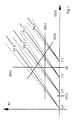
- Figure 1 depicts an ideal situation in which the cells associated with one level have exactly the same threshold voltage.
- the characteristics of the various cells associated with one level are bound to be different because the manufacture of integrated circuits cannot yield perfectly identical cells.
- Such characteristics will show a distribution, as indicated by dash lines and referenced DL0, DL1, DL2, DL3 in Figure 1, centered about an average characteristic indicated by a full line in Figure 1.
- the parameter that differentiates cells in the same distribution is the so-called "gain" of a cell.
- a read operation is to find the intersection of the characteristic of a cell to be read from with a read line;
- Figure 1 shows three viable read lines RD1, RD2, RD3.
- Figure 1 illustrates a typical situation where the supply voltage VCC is low, e.g. 2.2 volts. It should be understood that it is not necessary for the level spacings to be uniform as shown in Figure 1; on the contrary, the spacings can be optimized as most appropriate for reading.
- All three of the read lines RD1, RD2, RD3 require that a cell be supplied a higher voltage VGS than the supply voltage VCC.
- the lines RD2 and RD3 require that the value of the voltage VGS be controlled according to the current ID flowed between the drain and source terminals of the cell being read from; such lines should be positioned so that cells associated with different levels can be readily differentiated from one another.
- the read voltage VL should be at least higher than the level L2 -- the last-but-one from the bottom -- for otherwise the levels L2 and L3 cannot be differentiated according to the current ID. Having a higher voltage VL than the level L3 would be of little use, and could entail two disadvantages: on the one side, it becomes necessary to discriminate among four different values of the current ID, and on the other, when moving closer to the top, there would be a risk of confusing the levels, in particular LO and L1, due to their diverging characteristics.
- Figure 3 illustrates the effect of the write method on the threshold voltage distributions. Seeing that if a set of cells having a given distribution are subjected to precisely the same electrical "treatment", the distribution remains near-constant and shifts in voltage, an uncertitude about the extent of the shift will depend substantially on the write method.
- the effect from an initial level LO can be that shown in Figure 3 for different end levels L1, L2, L3.
- the multi-level memory circuit of this invention comprises:
- the write signals are electrically the same for all the cells, for a given information to be stored, they having widths of regulated value.
- each cell is to store an item of binary information corresponding to two bits, four different write signals would be needed, in theory.
- three discrete write signals can suffice because the fourth level is obtained by erasing.
- Such a memory circuit may require that the generating circuit be adapted to generate internally a write voltage having a value selectable from a number, three in this example, of discrete regulated values corresponding to the number, four in this example, of the discrete levels provided.
- the generating circuit could generate internally a number, three in this example, of write voltages having discrete regulated values corresponding to the number, four in this example, of the discrete levels provided. This alternative would be of advantage where several memory cells, possibly in separate arrays, must be programmed simultaneously.
- One way of generating regulated voltages is to use a linear type of voltage regulating circuit provided with a reference circuit for generating a stable reference voltage. Where more than one discrete write voltages are to be generated, a number of regulating circuits would be required.
- the regulator circuit may be advantageously arranged to include a voltage divider connected to the output of the reference circuit and having a plurality of center taps to provide a corresponding plurality of reference voltages.
- the reference voltages will be stable as well as tied to one another in stable ratii, determinable with great accuracy.
- the reference voltages so generated can be coupled selectively to a single regulator by means of controlled switches, or be coupled to discrete regulators.
- the level spacings are large. This can be accomplished by raising the voltage internally, where no external voltage source is available with a sufficiently high value.
- the generating circuit may include a voltage boosting circuit, adapted to output a write voltage exceeding the value of the supply voltage, and at least one voltage regulating circuit connected to the boosting circuit output. This requirement is specially stringent where the circuit is input no program voltage usually denoted by the reference VPP.
- the generating circuit may then be designed to generate a single write voltage pulse, for each write operation into a cell, whose amplitude corresponds to one of the regulated discrete write voltage values, specifically that associated with the information to be stored. In this case, it is convenient if the generating circuit can also regulate the pulse duration accurately; in this way, the write signals would be electrically identical for the various cells.
- the ideal number of discrete levels is four.
- the present circuit is applicable in particular to either EPROMs or OTP (One Time Programmable) memories (OTP memories being basically non-erasable EPROMs in that they lack a UV radiation transparent window), because the uncertitude in the distribution shift would be there only once. In fact, reprogramming is impossible, and erasing is either impossible or effected by a separate physical process. In this case, the number of levels can be raised to sixteen at an error rate which is still acceptable.
- OTP One Time Programmable
- the inventive memory circuit just described can be included in a semiconductor integrated electronic storage device or a generic semiconductor integrated electronic device in combination with at least one logic circuit connected to the memory circuit for reading and/or writing information.
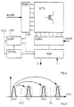
- the architecture of Figure 2 comprises a matrix MTX of memory cells organized into rows and columns. Connected thereto are a row decoder RDEC and a column decoder CDEC, which are input row RADR and column CADR addresses.
- the decoder CDEC is connected to an input/output managing circuit IOM which performs physically the read/write operations from/into the cells according to input signals I thereto and output signals O therefrom.
- the circuits in the architecture of Figure 2 need to be powered, which is accomplished by means of a power supply circuit ALIM receiving an external supply voltage VCC and external program voltage VPP.
- a power supply circuit ALIM receiving an external supply voltage VCC and external program voltage VPP.
- EPROMs are only supplied the voltage VPP during the off-line programming phase.
- the circuit ALIM supplies the decoder RDEC with a voltage VW for the word line which may be regarded as the read voltage during read operations, and the write voltage during write operations.
- the storage devices further require, and do include, a control circuit CNTRL which is supplied the voltage VCC to control the operation of the various internal circuits according to input control signals, not shown in Figure 2.
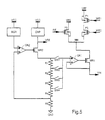
- circuits shown in Figures 4 and 5 illustrate two alternatives for a portion of the circuit ALIM which is utilized to generate the read or write voltage VW, as the case may be.
- the circuit of Figure 4 comprises three P-channel MOS transistors P1, P2, P3 acting as controlled switches.
- the first two, P1 and P2 have their main conduction paths connected in series between a node to be connected to a program voltage reference VPP and an internal node NN.
- the transistor P3 has its main conduction path connected between a node to be connected to a boosted voltage reference VEE and the internal node NN.
- the transistors P1 and P2 are input, to their control terminals, two write enable signals WE1 and WE2, respectively, which are synchronous with each other.
- the transistor P3 is input, to its control terminal, a read enable signal RE.
- the two transistors in series in the write leg serve to prevent spurious current flows between the references VEE and VPP.
- the circuit of Figure 4 further includes a conventional charge pump circuit CHP being input a supply voltage VCC and outputting the boosted voltage VEE.
- charge pump circuits include regulating arrangements to prevent the output voltage from overtaking predetermined limits.
- the output of the circuit CHP is connected to a first terminal of a zener diode DZ acting as a reference voltage generating circuit; the other terminal of the diode DZ is connected to ground, GND.
- the output of the circuit CHP is connected to a first end terminal of a voltage divider comprised of four resistors R1, R2, R3, R4 connected serially together, the second end terminal being connected to ground at GND.
- the center taps and first end terminal of the divider are connected to the non-inverting input of an operational amplifier OA1 via four controlled switches SW1, SW2, SW3, SW4, respectively.
- the voltage at the first end terminal, and therefore, the zener voltage is 12 volts
- the voltages at the center taps are 10, 8 and 7 volts, respectively.
- the 7-volt voltage is used for reading, and the other three for programming three different levels of the threshold voltage.
- the fourth level is provided by the erasing through exposure to UV radiation.
- the amplifier OA1 and a transistor MR1 form the essentials of a voltage regulator of the linear type.
- the gate terminal of the regulation transistor MR1 is controlled by the output from the amplifier OA1.
- the source terminal of the transistor MR1 is connected to the inverting input of the amplifier OA1, and its drain terminal is connected to the node NN.
- the output of the linear regulator is the source terminal of the transistor MR1.
- the circuit of Figure 5 is basically identical with the circuit of Figure 4, except that its reference circuit is different and comprises a conventional band-gap circuit BGR being supplied the voltage VCC. This circuit can output a truly stable voltage, typically of 2 volts.
- the output of the circuit BGR is connected to the non-inverting input of another operational amplifier OA2.
- the output of the amplifier OA2 is connected to the gate terminal of another regulation transistor MR2.
- the main conduction path of the transistor MR2 is interposed between the output of the circuit CHP and the divider input, i.e. the first end terminal thereof.
- the divider of Figure 5 has four center taps, because one of these, presenting a corresponding voltage to that from the circuit BGR, is to be connected to the inverting input of the amplifier OA2.
- the transistors P1, P2, P3 function to select the supply source from VPP or VEE, while preventing spurious current flows from occurring between the two sources.
- the transistor MR1 in cooperation with the amplifier OA1, sets the voltage VW to the voltage value present at the amplifier non-inverting terminal, i.e. the voltage value of the tap selected by means of the switches SW1,..., SW4.
- the voltage at the divider input corresponds to the voltage from the circuit CHP as stabilized by a suitable stabilizing circuit comprised of the zener diode DZ of Figure 4, the band-gap circuit BGR jointly with the amplifier OA2, and the transistor MR2 of Figure 5.
Landscapes
- Engineering & Computer Science (AREA)
- Computer Hardware Design (AREA)
- Read Only Memory (AREA)
Abstract
Description
Claims (9)
- A multi-level memory circuit for binary information, comprising:characterized in that said generating circuit (ALIM) includes a voltage booster circuit (CHP) adapted to output a higher voltage (VEE) than the value of the supply voltage (VCC), means (P1, P2, P3) for selecting a supply source between said program voltage (VPP) and said higher voltage (VEE) and at least one voltage regulating circuit (OA1, MR1) connected to the output of said booster circuit (CHP), said generating circuit (ALIM) being adapted to generate internally a write voltage (VW) or a number of write voltages having selectable values (SW1,...,SW4) from a number of discrete regulated values corresponding to the number of the discrete levels provided.a) a plurality (MTX) of memory cells, each adapted to store more than one item of binary information and comprised of at least one floating gate MOS transistor, the information stored in each cell corresponding to the level of the cell threshold voltage; andb) a write signal generating circuit (ALIM) for said cell plurality, adapted to receive as inputs a supply voltage (VCC) and a program voltage (VPP);
- A circuit according to either Claim 1, wherein said regulating circuit (OA1,MR1) is of the linear type and includes a reference circuit (DZ,BGR) for generating a stable reference voltage.
- A circuit according to Claim 2, wherein said regulating circuit includes a voltage divider (R1,...,R5) connected to the output of said reference circuit (DZ,BGR) and having a plurality of center taps for providing a corresponding plurality of reference voltages.
- A circuit according to either Claim 1, wherein said generating circuit (ALIM) is adapted to generate a single write voltage pulse for each write operation into a cell, the amplitude of said pulse corresponding to a write voltage value and associated with the information to be stored.
- A circuit according to Claim 4, wherein the generating circuit controls the duration of said pulse.
- A circuit according to one of the preceding claims, wherein the discrete levels provided are four in number.
- A circuit according to one of the preceding claims, wherein said cells are either EPROM or OTP cells.
- A semiconductor integrated electronic storage device comprising at least one memory circuit as claimed in one of the preceding claims.
- A semiconductor integrated electronic device comprising at least one memory circuit as claimed in one of the preceding claims, and a logic circuit connected to the memory circuit(s) for reading and/or writing information.
Priority Applications (1)
| Application Number | Priority Date | Filing Date | Title |
|---|---|---|---|
| EP96937494A EP0906623B1 (en) | 1996-06-20 | 1996-10-30 | Multi-level memory circuit with regulated writing voltage |
Applications Claiming Priority (4)
| Application Number | Priority Date | Filing Date | Title |
|---|---|---|---|
| EP96830354 | 1996-06-20 | ||
| EP96830354 | 1996-06-20 | ||
| PCT/IT1996/000199 WO1997049088A1 (en) | 1996-06-20 | 1996-10-30 | Multi-level memory circuit with regulated writing voltage |
| EP96937494A EP0906623B1 (en) | 1996-06-20 | 1996-10-30 | Multi-level memory circuit with regulated writing voltage |
Publications (2)
| Publication Number | Publication Date |
|---|---|
| EP0906623A1 EP0906623A1 (en) | 1999-04-07 |
| EP0906623B1 true EP0906623B1 (en) | 2001-01-03 |
Family
ID=8225945
Family Applications (1)
| Application Number | Title | Priority Date | Filing Date |
|---|---|---|---|
| EP96937494A Expired - Lifetime EP0906623B1 (en) | 1996-06-20 | 1996-10-30 | Multi-level memory circuit with regulated writing voltage |
Country Status (5)
| Country | Link |
|---|---|
| US (1) | US6097628A (en) |
| EP (1) | EP0906623B1 (en) |
| JP (1) | JP3968400B2 (en) |
| DE (1) | DE69611463T2 (en) |
| WO (1) | WO1997049088A1 (en) |
Families Citing this family (8)
| Publication number | Priority date | Publication date | Assignee | Title |
|---|---|---|---|---|
| US7225088B2 (en) * | 1998-09-16 | 2007-05-29 | Microchip Technology Incorporated | Programmable power supply and brownout detector for electronic equipment |
| US6304823B1 (en) * | 1998-09-16 | 2001-10-16 | Microchip Technology Incorporated | Microprocessor power supply system including a programmable power supply and a programmable brownout detector |
| KR100387267B1 (en) * | 1999-12-22 | 2003-06-11 | 주식회사 하이닉스반도체 | Multi-level flash EEPROM cell and method of manufacturing the same |
| DE60025697D1 (en) * | 2000-02-08 | 2006-04-13 | St Microelectronics Srl | Booster device |
| KR100443792B1 (en) * | 2001-10-15 | 2004-08-09 | 주식회사 하이닉스반도체 | Circuit for programming a flash EEPROM and method of programming a flash EEPROM using the same |
| US6614210B2 (en) * | 2001-12-18 | 2003-09-02 | Intel Corporation | Variable voltage source for a flash device operating from a power-supply-in-package (PSIP) |
| US6754103B2 (en) * | 2002-11-04 | 2004-06-22 | Silicon Storage Technology, Inc. | Method and apparatus for programming and testing a non-volatile memory cell for storing multibit states |
| JP6017291B2 (en) * | 2012-12-10 | 2016-10-26 | エスアイアイ・セミコンダクタ株式会社 | Nonvolatile memory circuit |
Citations (1)
| Publication number | Priority date | Publication date | Assignee | Title |
|---|---|---|---|---|
| EP0656629A2 (en) * | 1993-12-01 | 1995-06-07 | Advanced Micro Devices, Inc. | Gate power supply |
Family Cites Families (9)
| Publication number | Priority date | Publication date | Assignee | Title |
|---|---|---|---|---|
| DE3205476A1 (en) * | 1982-02-16 | 1983-08-25 | Siemens AG, 1000 Berlin und 8000 München | WORDING ELECTRICALLY REPROGRAMMABLE NON-VOLATILE STORAGE AND USE OF SUCH A STORAGE |
| JPH02260298A (en) * | 1989-03-31 | 1990-10-23 | Oki Electric Ind Co Ltd | Non-volatile multilevel memory device |
| JP3379761B2 (en) * | 1991-07-02 | 2003-02-24 | 株式会社日立製作所 | Non-volatile storage device |
| JPH05151789A (en) * | 1991-11-29 | 1993-06-18 | Nec Corp | Electrically writable and batch erasable nonvolatile semiconductor memory device |
| US5412601A (en) * | 1992-08-31 | 1995-05-02 | Nippon Steel Corporation | Non-volatile semiconductor memory device capable of storing multi-value data in each memory cell |
| US5694356A (en) * | 1994-11-02 | 1997-12-02 | Invoice Technology, Inc. | High resolution analog storage EPROM and flash EPROM |
| EP0715312B1 (en) * | 1994-11-30 | 2002-10-23 | STMicroelectronics S.r.l. | Monolitically integrated generator of a plurality of voltage values |
| KR100221523B1 (en) * | 1995-08-31 | 1999-09-15 | 다카노 야스아키 | Non-volatile multi-state memory apparatus having memory cell which can store multi- state information |
| US5745409A (en) * | 1995-09-28 | 1998-04-28 | Invox Technology | Non-volatile memory with analog and digital interface and storage |
-
1996
- 1996-10-30 JP JP50263798A patent/JP3968400B2/en not_active Expired - Fee Related
- 1996-10-30 DE DE69611463T patent/DE69611463T2/en not_active Expired - Fee Related
- 1996-10-30 EP EP96937494A patent/EP0906623B1/en not_active Expired - Lifetime
- 1996-10-30 WO PCT/IT1996/000199 patent/WO1997049088A1/en not_active Ceased
- 1996-10-30 US US09/202,656 patent/US6097628A/en not_active Expired - Lifetime
Patent Citations (1)
| Publication number | Priority date | Publication date | Assignee | Title |
|---|---|---|---|---|
| EP0656629A2 (en) * | 1993-12-01 | 1995-06-07 | Advanced Micro Devices, Inc. | Gate power supply |
Also Published As
| Publication number | Publication date |
|---|---|
| DE69611463D1 (en) | 2001-02-08 |
| DE69611463T2 (en) | 2001-05-03 |
| JP2002514337A (en) | 2002-05-14 |
| WO1997049088A1 (en) | 1997-12-24 |
| EP0906623A1 (en) | 1999-04-07 |
| US6097628A (en) | 2000-08-01 |
| JP3968400B2 (en) | 2007-08-29 |
Similar Documents
| Publication | Publication Date | Title |
|---|---|---|
| JP3737525B2 (en) | Semiconductor memory device | |
| US7002869B2 (en) | Voltage regulator circuit | |
| US6266270B1 (en) | Non-volatile semiconductor memory and programming method of the same | |
| US5835420A (en) | Node-precise voltage regulation for a MOS memory system | |
| US20080253182A1 (en) | Nand flash memory device and programming method | |
| US5801991A (en) | Deselected word line that floats during MLC programming of a flash memory | |
| US6292396B1 (en) | Method and device for the programming of an electrically programmable non-volatile memory for improved reliability | |
| KR100384803B1 (en) | Voltage generating circuit for generating different voltages | |
| JPH10228784A (en) | Nonvolatile semiconductor memory device | |
| US6735121B2 (en) | Nonvolatile memory system having status register for rewrite control | |
| EP0906623B1 (en) | Multi-level memory circuit with regulated writing voltage | |
| US6222771B1 (en) | Unified program method and circuitry in flash EEPROM | |
| US20070242541A1 (en) | Sense amplifier with reduced current consumption for semiconductors memories | |
| US6101121A (en) | Multi-level memory circuit with regulated reading voltage | |
| US6812747B2 (en) | Supply voltage comparator | |
| EP1331644B1 (en) | Regulation method for the source voltage in a nonvolatile memory cell during programming and corresponding program circuit | |
| US6829169B2 (en) | Electrically erasable and programmable memory comprising an internal supply voltage management device | |
| EP0899742B1 (en) | Method and circuit for generating a gate voltage in non-volatile memory devices | |
| US6606266B2 (en) | Nonvolatile semiconductor memory device capable of writing multilevel data at high rate | |
| KR100572302B1 (en) | A flash memory device and method for programming the same | |
| JP3591849B2 (en) | Storage device and method of operating the storage device | |
| EP1883076B1 (en) | Method of programming cells of a NAND memory device | |
| US6028793A (en) | High voltage driver circuit for a decoding circuit in multilevel non-volatile memory devices | |
| US6934185B2 (en) | Programming method for non volatile multilevel memory cells and corresponding programming circuit |
Legal Events
| Date | Code | Title | Description |
|---|---|---|---|
| PUAI | Public reference made under article 153(3) epc to a published international application that has entered the european phase |
Free format text: ORIGINAL CODE: 0009012 |
|
| 17P | Request for examination filed |
Effective date: 19981221 |
|
| AK | Designated contracting states |
Kind code of ref document: A1 Designated state(s): DE FR GB IT |
|
| 17Q | First examination report despatched |
Effective date: 19990406 |
|
| GRAG | Despatch of communication of intention to grant |
Free format text: ORIGINAL CODE: EPIDOS AGRA |
|
| GRAG | Despatch of communication of intention to grant |
Free format text: ORIGINAL CODE: EPIDOS AGRA |
|
| GRAH | Despatch of communication of intention to grant a patent |
Free format text: ORIGINAL CODE: EPIDOS IGRA |
|
| GRAH | Despatch of communication of intention to grant a patent |
Free format text: ORIGINAL CODE: EPIDOS IGRA |
|
| ITF | It: translation for a ep patent filed | ||
| GRAA | (expected) grant |
Free format text: ORIGINAL CODE: 0009210 |
|
| AK | Designated contracting states |
Kind code of ref document: B1 Designated state(s): DE FR GB IT |
|
| REF | Corresponds to: |
Ref document number: 69611463 Country of ref document: DE Date of ref document: 20010208 |
|
| ET | Fr: translation filed | ||
| PLBE | No opposition filed within time limit |
Free format text: ORIGINAL CODE: 0009261 |
|
| STAA | Information on the status of an ep patent application or granted ep patent |
Free format text: STATUS: NO OPPOSITION FILED WITHIN TIME LIMIT |
|
| REG | Reference to a national code |
Ref country code: GB Ref legal event code: IF02 |
|
| 26N | No opposition filed | ||
| PGFP | Annual fee paid to national office [announced via postgrant information from national office to epo] |
Ref country code: DE Payment date: 20040924 Year of fee payment: 9 |
|
| PG25 | Lapsed in a contracting state [announced via postgrant information from national office to epo] |
Ref country code: IT Free format text: LAPSE BECAUSE OF NON-PAYMENT OF DUE FEES Effective date: 20051030 |
|
| PG25 | Lapsed in a contracting state [announced via postgrant information from national office to epo] |
Ref country code: DE Free format text: LAPSE BECAUSE OF NON-PAYMENT OF DUE FEES Effective date: 20060503 |
|
| PGFP | Annual fee paid to national office [announced via postgrant information from national office to epo] |
Ref country code: GB Payment date: 20080926 Year of fee payment: 13 |
|
| PGFP | Annual fee paid to national office [announced via postgrant information from national office to epo] |
Ref country code: FR Payment date: 20081028 Year of fee payment: 13 |
|
| REG | Reference to a national code |
Ref country code: FR Ref legal event code: ST Effective date: 20100630 |
|
| PG25 | Lapsed in a contracting state [announced via postgrant information from national office to epo] |
Ref country code: FR Free format text: LAPSE BECAUSE OF NON-PAYMENT OF DUE FEES Effective date: 20091102 |
|
| PG25 | Lapsed in a contracting state [announced via postgrant information from national office to epo] |
Ref country code: GB Free format text: LAPSE BECAUSE OF NON-PAYMENT OF DUE FEES Effective date: 20091030 |