EP0906622B1 - Multi-level memory circuit with regulated reading voltage - Google Patents
Multi-level memory circuit with regulated reading voltage Download PDFInfo
- Publication number
- EP0906622B1 EP0906622B1 EP96937493A EP96937493A EP0906622B1 EP 0906622 B1 EP0906622 B1 EP 0906622B1 EP 96937493 A EP96937493 A EP 96937493A EP 96937493 A EP96937493 A EP 96937493A EP 0906622 B1 EP0906622 B1 EP 0906622B1
- Authority
- EP
- European Patent Office
- Prior art keywords
- voltage
- circuit
- level
- read
- memory
- Prior art date
- Legal status (The legal status is an assumption and is not a legal conclusion. Google has not performed a legal analysis and makes no representation as to the accuracy of the status listed.)
- Expired - Lifetime
Links
Images


Classifications
-
- G—PHYSICS
- G11—INFORMATION STORAGE
- G11C—STATIC STORES
- G11C11/00—Digital stores characterised by the use of particular electric or magnetic storage elements; Storage elements therefor
- G11C11/56—Digital stores characterised by the use of particular electric or magnetic storage elements; Storage elements therefor using storage elements with more than two stable states represented by steps, e.g. of voltage, current, phase, frequency
- G11C11/5621—Digital stores characterised by the use of particular electric or magnetic storage elements; Storage elements therefor using storage elements with more than two stable states represented by steps, e.g. of voltage, current, phase, frequency using charge storage in a floating gate
- G11C11/5642—Sensing or reading circuits; Data output circuits
-
- G—PHYSICS
- G11—INFORMATION STORAGE
- G11C—STATIC STORES
- G11C16/00—Erasable programmable read-only memories
- G11C16/02—Erasable programmable read-only memories electrically programmable
- G11C16/06—Auxiliary circuits, e.g. for writing into memory
- G11C16/30—Power supply circuits
-
- G—PHYSICS
- G11—INFORMATION STORAGE
- G11C—STATIC STORES
- G11C5/00—Details of stores covered by group G11C11/00
- G11C5/14—Power supply arrangements, e.g. power down, chip selection or deselection, layout of wirings or power grids, or multiple supply levels
- G11C5/145—Applications of charge pumps; Boosted voltage circuits; Clamp circuits therefor
Definitions
- This invention relates to a multi-level type of memory circuit for binary information, according to the preamble of Claim 1.
- Non-volatile Memories of this type are usually termed “non-volatile” because of their capability to retain stored information over very long time periods, even in the absence of a power supply, and include the EPROM, EEPROM, and FLASH EEPROM families.
- All these read circuits and methods provide for the application, between the gate and source terminals of a cell being read, of a read voltage from a row decoding circuit which is powered by a supply circuit.
- the current flowing into the channel of the MOS transistor, or the voltage at the drain terminal, for example, is then measured and compared to currents or voltages having reference values.
- a power supply circuit for a row decoding circuit which suits the effectuation of read, write, and erase operations on two-level non-volatile memories.
- This power supply circuit comprises a read voltage generating section effective on request to output a voltage corresponding to the supply voltage, a write voltage generating section effective on request to output a boosted positive voltage with respect to the supply voltage, and an erase voltage generating section effective on request to output a highly negative voltage with respect to ground.
- the US patent No. 5,218,569 relates to a non-volatile memory device of the multi-level type including comparator means for generating a control signal indicative of the memory state.
- the present invention sets out from the idea of having the different threshold voltage levels for multi-level non-volatile memories sufficiently spaced apart to make the read circuit significantly less critical.
- the idea underlying this invention is one of having the gate-source voltage VGS thoroughly under careful control, so that current and/or voltage readings can be performed with the utmost accuracy.
- Figure 1 depicts an ideal situation in which the cells associated with one level have exactly the same threshold voltage.
- the characteristics of the various cells associated with one level are bound to be different because the manufacture of integrated circuits cannot yield perfectly identical cells.
- Such characteristics will show a distribution, as indicated by dash lines and referenced DL0, DL1, DL2, DL3 in Figure 1, centered about an average characteristic indicated by a full line in Figure 1.
- the parameter that differentiates cells in the same distribution is the so-called "gain" of a cell.
- a read operation is to find the intersection of the characteristic of a cell to be read from with a read line;
- Figure 1 shows three viable read lines RD1, RD2, RD3.
- Figure 1 illustrates a typical situation where the supply voltage VCC is low, e.g. 2.2 volts. It should be understood that it is not necessary for the level spacings to be uniform as shown in Figure 1; on the contrary, the spacings can be optimized as most appropriate for reading.
- All three of the read lines RD1, RD2, RD3 require that a cell be supplied a higher voltage VGS than the supply voltage VCC.
- the lines RD2 and RD3 require that the value of the voltage VGS be controlled according to the current ID flowed between the drain and source terminals of the cell being read from; such lines should be positioned so that cells associated with different levels can be readily differentiated from one another.
- the read voltage VL should be at least higher than the level L2 -- the last-but-one from the bottom -- for otherwise the levels L2 and L3 cannot be differentiated according to the current ID. Having a higher voltage VL than the level L3 would be of little use, and could entail two disadvantages: on the one side, it becomes necessary to discriminate among four different values of the current ID, and on the other, in proceeding toward the top, there would be a risk of confusing the levels, in particular L0 and L1, due to their diverging characteristics.
- Figure 3 illustrates the effect of the write method on the threshold voltage distributions. Seeing that if a set of cells having a given distribution are subjected to precisely the same electrical "treatment", the distribution remains near-constant and shifts in voltage, an uncertitude about the extent of the shift will depend substantially on the write method.
- the effect from an initial level L0 can be that shown in Figure 3 for different end levels L1, L2, L3.
- the multi-level memory circuit of this invention comprises:
- Such a memory circuit would include a voltage boosting circuit adapted to generate a read voltage having a higher value than the value of the supply voltage.
- the various levels are free to be associated with threshold voltage values without undergoing restrictions from the value of the read voltage, and this independently of the read line selected.
- the value of the read voltage can be an intermediate one between the highest level and the next lower level of the threshold voltage.
- the ideal number of discrete levels is four.
- the voltage boosting circuit is to generate a read voltage with a regulated value. This can be accomplished using a linear type of voltage regulator having a reference circuit to provide a stable reference voltage.
- the present circuit is applicable in particular to either EPROMs or OTP (One Time Programmable) memories (OTP memories being basically non-erasable EPROMs in that they lack a UV radiation transparent window), because the uncertitude about the distribution shift would be there only once.
- OTP memories One Time Programmable memories
- reprogramming is impossible, and erasing either impossible or effected by a separate physical process, and since programming can be performed theoretically with great accuracy because off-line, in the last-mentioned case the number of the levels can be raised to sixteen, at an error rate which is still acceptable.
- the inventive memory circuit just described can be included in a semiconductor integrated electronic storage device or a generic semiconductor integrated electronic device in combination with at least one logic circuit connected to the memory circuit for reading and/or writing information.
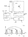
- the architecture of Figure 2 comprises a matrix MTX of memory cells organized into rows and columns. Connected thereto are a row decoder RDEC and a column decoder CDEC, which are input row RADR and column CADR addresses, respectively.
- the decoder CDEC is connected to an input/output managing circuit IOM which performs physically the read/write operations from/into the cells according to input signals I thereto and output signals O therefrom.
- the circuits in the architecture of Figure 2 need to be powered, which is accomplished by means of a power supply circuit ALIM receiving an external supply voltage VCC and external program voltage VPP.
- a power supply circuit ALIM receiving an external supply voltage VCC and external program voltage VPP.
- EPROMs are only supplied the voltage VPP during the off-line programming phase.
- the circuit ALIM supplies the decoder RDEC with a voltage VW for the word line which may be regarded as the read voltage during read operations, and the write voltage during write operations.
- the storage devices further require, and do include, a control circuit CNTRL which is supplied the voltage VCC to control the operation of the various internal circuits according to input control signals, not shown in Figure 2.
- circuits shown in Figures 4 and 5 illustrate two alternatives for a portion of the circuit ALIM which is utilized to generate the read or write voltage VW, as the case may be.
- the circuit of Figure 4 comprises three P-channel MOS transistors P1, P2, P3 serving as controlled switches.
- the first two, P1 and P2 have their main conduction paths connected in series between a node to be connected to a program voltage reference VPP and an internal node NN.
- the transistor P3 has its main conduction path connected between a node to be connected to a boosted voltage reference VEE and the internal node NN.
- the transistors P1 and P2 are input, to their control terminals, two write enable signals WE1 and WE2, respectively, which are synchronous with each other.
- the transistor P3 is input, to its control terminal, a read enable signal RE.
- the two transistors in series in the write leg serve to prevent any spurious current flows between the references VEE and VPP.
- the circuit of Figure 4 further includes a conventional charge pump circuit CHP being input a supply voltage VCC and outputting the boosted voltage VEE.
- charge pump circuits include regulating arrangements to prevent the output voltage from overtaking predetermined limits.
- the output of the circuit CHP is connected to a first terminal of a zener diode DZ acting as a reference voltage generating circuit; the other terminal of the diode DZ is connected to ground, GND.
- the output of the circuit CHP is connected to a first end terminal of a voltage divider comprised of four resistors R1, R2, R3, R4 connected serially together, the second end terminal being connected to ground at GND.
- the center taps and first end terminal of the divider are connected to the non-inverting input of an operational amplifier OA1 via four controlled switches SW1, SW2, SW3, SW4, respectively.
- the voltage at the first end terminal, and therefore, the zener voltage is 12 volts
- the voltages at the center taps are 10, 8 and 7 volts, respectively.
- the 7-volt voltage is used for reading, and the other three for programming three different levels of the threshold voltage.
- the fourth level is provided by the erasing through exposure to UV radiation.
- the amplifier OA1 and a transistor MR1 form the essentials of a voltage regulator of the linear type.
- the gate terminal of the regulation transistor MR1 is controlled by the output from the amplifier OA1.
- the source terminal of the transistor MR1 is connected to the inverting input of the amplifier OA1, and its drain terminal is connected to the node NN.
- the output of the linear regulator is the source terminal of the transistor MR1.
- the circuit of Figure 5 is basically identical with the circuit of Figure 4, except that its reference circuit is different and comprises a conventional band-gap circuit BGR being supplied the voltage VCC. This circuit can output a truly stable voltage, typically of 2 volts.
- the output of the circuit BGR is connected to the non-inverting input of another operational amplifier OA2.
- the output of the amplifier OA2 is connected to the gate terminal of another regulation transistor MR2.
- the main conduction path of the transistor MR2 is interposed between the output of the circuit CHP and the divider input, i.e. the first end terminal thereof.
- the divider of Figure 5 has four center taps, because one of these, presenting a corresponding voltage to that from the circuit BGR, is to be connected to the inverting input of the amplifier OA2.
- the transistors P1, P2, P3 function to select the supply source from VPP or VEE, while preventing spurious current flows from occurring between the two sources.
- the transistor MR1 in cooperation with the amplifier OA1, sets the voltage VW to the voltage value present at the amplifier non-inverting terminal, i.e. the voltage value of the tap selected by means of the switches SW1,..., SW4.
- the voltage at the divider input corresponds to the voltage from the circuit CHP as stabilized by a suitable stabilizing circuit comprised of the zener diode DZ of Figure 4, the band-gap circuit BGR jointly with the amplifier OA2, and the transistor MR2 of Figure 5.
Landscapes
- Engineering & Computer Science (AREA)
- Computer Hardware Design (AREA)
- Read Only Memory (AREA)
Abstract
Description
Claims (7)
- A multi-level memory circuit for binary information, comprising:characterized in that said generating circuit (ALIM) includes a voltage boosting circuit (CHP) adapted to output a higher voltage (VEE) than the value of the supply voltage (VCC), means (P1, P2, P3) for selecting a supply voltage between said program voltage (VPP) and said higher voltage (VEE) and a voltage regulating circuit (OA1, MR1) connected to the output of said booster circuit (CHP), said generating circuit (ALIM) being adapted to generate a read voltage (VW) having intermediate value between the highest threshold voltage level (L3) and the next lower level (L2) thereof.a) a plurality (MTX) of memory cells, each adapted to store more than one item of binary information and comprised of at least one floating gate MOS transistor, the information stored in each cell corresponding to the level of the cell threshold voltage; andb) a read voltage generating circuit (ALIM) for said cell plurality, adapted to receive as inputs a supply voltage (VCC) and a program voltage (VPP);
- A circuit according to either Claim 1, wherein the discrete levels are four in number.
- A circuit according to one of the preceding claims, wherein the voltage boosting circuit is adapted to generate a read voltage (VW) with a regulated value.
- A circuit according to Claim 3, wherein the voltage regulating circuit (OA1,MR1) is of the linear type and has a reference circuit (DZ,BGR) for generating a stable reference voltage.
- A circuit according to one of the preceding claims, wherein said cells are either EPROM or OTP cells.
- A semiconductor integrated electronic storage device comprising at least one memory circuit as claimed in one of the preceding claims.
- A semiconductor integrated electronic device comprising at least one memory circuit as claimed in one of the preceding claims, and a logic circuit connected to the memory circuit(s) for reading and/or writing information.
Priority Applications (1)
| Application Number | Priority Date | Filing Date | Title |
|---|---|---|---|
| EP96937493A EP0906622B1 (en) | 1996-06-20 | 1996-10-30 | Multi-level memory circuit with regulated reading voltage |
Applications Claiming Priority (4)
| Application Number | Priority Date | Filing Date | Title |
|---|---|---|---|
| EP96830355 | 1996-06-20 | ||
| EP96830355 | 1996-06-20 | ||
| EP96937493A EP0906622B1 (en) | 1996-06-20 | 1996-10-30 | Multi-level memory circuit with regulated reading voltage |
| PCT/IT1996/000198 WO1997049087A1 (en) | 1996-06-20 | 1996-10-30 | Multi-level memory circuit with regulated reading voltage |
Publications (2)
| Publication Number | Publication Date |
|---|---|
| EP0906622A1 EP0906622A1 (en) | 1999-04-07 |
| EP0906622B1 true EP0906622B1 (en) | 2001-01-10 |
Family
ID=8225946
Family Applications (1)
| Application Number | Title | Priority Date | Filing Date |
|---|---|---|---|
| EP96937493A Expired - Lifetime EP0906622B1 (en) | 1996-06-20 | 1996-10-30 | Multi-level memory circuit with regulated reading voltage |
Country Status (5)
| Country | Link |
|---|---|
| US (1) | US6101121A (en) |
| EP (1) | EP0906622B1 (en) |
| JP (1) | JP4007457B2 (en) |
| DE (1) | DE69611550T2 (en) |
| WO (1) | WO1997049087A1 (en) |
Families Citing this family (8)
| Publication number | Priority date | Publication date | Assignee | Title |
|---|---|---|---|---|
| DE60025697D1 (en) * | 2000-02-08 | 2006-04-13 | St Microelectronics Srl | Booster device |
| JP4149637B2 (en) * | 2000-05-25 | 2008-09-10 | 株式会社東芝 | Semiconductor device |
| US20040023816A1 (en) * | 2002-08-01 | 2004-02-05 | Burts Boyce Donald | Hydraulic fracturing additive, hydraulic fracturing treatment fluid made therefrom, and method of hydraulically fracturing a subterranean formation |
| KR100568116B1 (en) * | 2004-09-13 | 2006-04-05 | 삼성전자주식회사 | Flash memory device with voltage regulation means |
| ITMI20050798A1 (en) | 2005-05-03 | 2006-11-04 | Atmel Corp | METHOD AND SYSTEM FOR THE GENERATION OF PROGRAMMING IMPULSES DURING THE PROGRAMMING OF NON-VOLATILE ELECTRONIC DEVICES |
| US8630125B2 (en) | 2011-06-02 | 2014-01-14 | Micron Technology, Inc. | Memory cell sensing using a boost voltage |
| FR3012654A1 (en) | 2013-10-25 | 2015-05-01 | St Microelectronics Rousset | METHOD OF WRITING AND READING A DELEGALLY PROGRAMMABLE AND DELEGALLY MULTI-LEVEL DEAD MEMORY AND CORRESPONDING MEMORY DEVICE |
| US11271566B2 (en) * | 2018-12-14 | 2022-03-08 | Integrated Device Technology, Inc. | Digital logic compatible inputs in compound semiconductor circuits |
Citations (1)
| Publication number | Priority date | Publication date | Assignee | Title |
|---|---|---|---|---|
| US5218569A (en) * | 1991-02-08 | 1993-06-08 | Banks Gerald J | Electrically alterable non-volatile memory with n-bits per memory cell |
Family Cites Families (3)
| Publication number | Priority date | Publication date | Assignee | Title |
|---|---|---|---|---|
| US5414669A (en) * | 1993-09-10 | 1995-05-09 | Intel Corporation | Method and apparatus for programming and erasing flash EEPROM memory arrays utilizing a charge pump circuit |
| US5511026A (en) * | 1993-12-01 | 1996-04-23 | Advanced Micro Devices, Inc. | Boosted and regulated gate power supply with reference tracking for multi-density and low voltage supply memories |
| EP0715312B1 (en) * | 1994-11-30 | 2002-10-23 | STMicroelectronics S.r.l. | Monolitically integrated generator of a plurality of voltage values |
-
1996
- 1996-10-30 JP JP50263698A patent/JP4007457B2/en not_active Expired - Fee Related
- 1996-10-30 EP EP96937493A patent/EP0906622B1/en not_active Expired - Lifetime
- 1996-10-30 US US09/202,657 patent/US6101121A/en not_active Expired - Lifetime
- 1996-10-30 DE DE69611550T patent/DE69611550T2/en not_active Expired - Fee Related
- 1996-10-30 WO PCT/IT1996/000198 patent/WO1997049087A1/en not_active Ceased
Patent Citations (1)
| Publication number | Priority date | Publication date | Assignee | Title |
|---|---|---|---|---|
| US5218569A (en) * | 1991-02-08 | 1993-06-08 | Banks Gerald J | Electrically alterable non-volatile memory with n-bits per memory cell |
Non-Patent Citations (2)
| Title |
|---|
| BLEIKER, MELCHIOR: "A Four-state EEPROM Using Floating-Gate Memory Cells", IEEE JOURNAL OF SOLID-STATE CIRCUITS., vol. SC22, no. 3, NEW YORK US, pages 460 - 463 * |
| RICH: "A Survey of Multivalued Memories", IEEE TRANSACTIONS ON COMPUTERS, vol. C-35, no. 2, NEW YORK US, pages 99 - 106 * |
Also Published As
| Publication number | Publication date |
|---|---|
| JP4007457B2 (en) | 2007-11-14 |
| US6101121A (en) | 2000-08-08 |
| DE69611550D1 (en) | 2001-02-15 |
| WO1997049087A1 (en) | 1997-12-24 |
| DE69611550T2 (en) | 2001-04-26 |
| JP2002514336A (en) | 2002-05-14 |
| EP0906622A1 (en) | 1999-04-07 |
Similar Documents
| Publication | Publication Date | Title |
|---|---|---|
| US7002869B2 (en) | Voltage regulator circuit | |
| US7898869B2 (en) | Word line voltage generator and flash memory device including the same, and method of generating word line voltage thereof | |
| US6266270B1 (en) | Non-volatile semiconductor memory and programming method of the same | |
| EP1620860B1 (en) | Memory with uniform read and verification threshold | |
| US5712815A (en) | Multiple bits per-cell flash EEPROM capable of concurrently programming and verifying memory cells and reference cells | |
| US7697327B2 (en) | NAND flash memory device and programming method | |
| KR100512181B1 (en) | Flash memory device having multi-level cell and method for its reading operation and program operation | |
| JP3652826B2 (en) | Multi-value storage nonvolatile semiconductor memory | |
| US5847992A (en) | Multi-level non-volatile semiconductor memory device having improved multi-level data storing circuits | |
| EP1615227A2 (en) | Multilevel semiconductor memory device | |
| EP1729302B1 (en) | A circuit for retrieving data stored in semiconductor memory cells | |
| US7460402B2 (en) | Semiconductor memory device which generates voltages corresponding to a plurality of threshold voltages | |
| US6166950A (en) | Nonvolatile semiconductor storage device | |
| US6735121B2 (en) | Nonvolatile memory system having status register for rewrite control | |
| EP0906622B1 (en) | Multi-level memory circuit with regulated reading voltage | |
| US7826284B2 (en) | Sense amplifier circuit and method for semiconductor memories with reduced current consumption | |
| US6097628A (en) | Multi-level memory circuit with regulated writing voltage | |
| US6812747B2 (en) | Supply voltage comparator | |
| US6829169B2 (en) | Electrically erasable and programmable memory comprising an internal supply voltage management device | |
| US7529133B2 (en) | Nonvolatile semiconductor storage apparatus and readout method | |
| US7633815B2 (en) | Flexible word line boosting across VCC supply | |
| EP0899742B1 (en) | Method and circuit for generating a gate voltage in non-volatile memory devices | |
| CN111081304B (en) | Memory device and programming method thereof | |
| US6028793A (en) | High voltage driver circuit for a decoding circuit in multilevel non-volatile memory devices | |
| US6934185B2 (en) | Programming method for non volatile multilevel memory cells and corresponding programming circuit |
Legal Events
| Date | Code | Title | Description |
|---|---|---|---|
| PUAI | Public reference made under article 153(3) epc to a published international application that has entered the european phase |
Free format text: ORIGINAL CODE: 0009012 |
|
| 17P | Request for examination filed |
Effective date: 19981221 |
|
| AK | Designated contracting states |
Kind code of ref document: A1 Designated state(s): DE FR GB IT |
|
| 17Q | First examination report despatched |
Effective date: 19990406 |
|
| GRAG | Despatch of communication of intention to grant |
Free format text: ORIGINAL CODE: EPIDOS AGRA |
|
| GRAG | Despatch of communication of intention to grant |
Free format text: ORIGINAL CODE: EPIDOS AGRA |
|
| GRAH | Despatch of communication of intention to grant a patent |
Free format text: ORIGINAL CODE: EPIDOS IGRA |
|
| GRAH | Despatch of communication of intention to grant a patent |
Free format text: ORIGINAL CODE: EPIDOS IGRA |
|
| ITF | It: translation for a ep patent filed | ||
| GRAA | (expected) grant |
Free format text: ORIGINAL CODE: 0009210 |
|
| AK | Designated contracting states |
Kind code of ref document: B1 Designated state(s): DE FR GB IT |
|
| REF | Corresponds to: |
Ref document number: 69611550 Country of ref document: DE Date of ref document: 20010215 |
|
| ET | Fr: translation filed | ||
| PLBE | No opposition filed within time limit |
Free format text: ORIGINAL CODE: 0009261 |
|
| STAA | Information on the status of an ep patent application or granted ep patent |
Free format text: STATUS: NO OPPOSITION FILED WITHIN TIME LIMIT |
|
| REG | Reference to a national code |
Ref country code: GB Ref legal event code: IF02 |
|
| 26N | No opposition filed | ||
| PGFP | Annual fee paid to national office [announced via postgrant information from national office to epo] |
Ref country code: DE Payment date: 20040924 Year of fee payment: 9 |
|
| PG25 | Lapsed in a contracting state [announced via postgrant information from national office to epo] |
Ref country code: IT Free format text: LAPSE BECAUSE OF NON-PAYMENT OF DUE FEES;WARNING: LAPSES OF ITALIAN PATENTS WITH EFFECTIVE DATE BEFORE 2007 MAY HAVE OCCURRED AT ANY TIME BEFORE 2007. THE CORRECT EFFECTIVE DATE MAY BE DIFFERENT FROM THE ONE RECORDED. Effective date: 20051030 |
|
| PG25 | Lapsed in a contracting state [announced via postgrant information from national office to epo] |
Ref country code: DE Free format text: LAPSE BECAUSE OF NON-PAYMENT OF DUE FEES Effective date: 20060503 |
|
| PGFP | Annual fee paid to national office [announced via postgrant information from national office to epo] |
Ref country code: GB Payment date: 20080926 Year of fee payment: 13 |
|
| PGFP | Annual fee paid to national office [announced via postgrant information from national office to epo] |
Ref country code: FR Payment date: 20081028 Year of fee payment: 13 |
|
| REG | Reference to a national code |
Ref country code: FR Ref legal event code: ST Effective date: 20100630 |
|
| PG25 | Lapsed in a contracting state [announced via postgrant information from national office to epo] |
Ref country code: FR Free format text: LAPSE BECAUSE OF NON-PAYMENT OF DUE FEES Effective date: 20091102 |
|
| PG25 | Lapsed in a contracting state [announced via postgrant information from national office to epo] |
Ref country code: GB Free format text: LAPSE BECAUSE OF NON-PAYMENT OF DUE FEES Effective date: 20091030 |