EP0903884A2 - Phase estimating circuit and demodulating circuit - Google Patents
Phase estimating circuit and demodulating circuit Download PDFInfo
- Publication number
- EP0903884A2 EP0903884A2 EP98111262A EP98111262A EP0903884A2 EP 0903884 A2 EP0903884 A2 EP 0903884A2 EP 98111262 A EP98111262 A EP 98111262A EP 98111262 A EP98111262 A EP 98111262A EP 0903884 A2 EP0903884 A2 EP 0903884A2
- Authority
- EP
- European Patent Office
- Prior art keywords
- circuit
- phase
- dft
- output
- input signal
- Prior art date
- Legal status (The legal status is an assumption and is not a legal conclusion. Google has not performed a legal analysis and makes no representation as to the accuracy of the status listed.)
- Granted
Links
Images


Classifications
-
- H—ELECTRICITY
- H04—ELECTRIC COMMUNICATION TECHNIQUE
- H04L—TRANSMISSION OF DIGITAL INFORMATION, e.g. TELEGRAPHIC COMMUNICATION
- H04L7/00—Arrangements for synchronising receiver with transmitter
- H04L7/02—Speed or phase control by the received code signals, the signals containing no special synchronisation information
- H04L7/027—Speed or phase control by the received code signals, the signals containing no special synchronisation information extracting the synchronising or clock signal from the received signal spectrum, e.g. by using a resonant or bandpass circuit
Definitions
- the invention relates to clock recovery by a demodulator in a data communication system.
- a conventional clock recovery circuit is proposed to recover a clock by determining a phase component of an input signal's clock by Fourier transformation and performing a reverse modulation of the determined phase component.
- Fig. 12 shows an example of configuration of a conventional clock recovery circuit, which is disclosed in, for example, Japanese Patent Laid-Open Publication No. Hei 6-232933, "Clock Recovery Circuit".
- Fig. 12 shows an example of configuration of a conventional clock recovery circuit, which is disclosed in, for example, Japanese Patent Laid-Open Publication No. Hei 6-232933, "Clock Recovery Circuit".
- reference numeral 101 denotes an input terminal
- 103 and 104 multipliers for multiplying an input signal by a twiddle factor (cos or -sin component) for the Fourier transform
- 105 and 106 low pass filters for averaging outputs from the multiplier 103 or 104
- 107 a multiplier for multiplying output from the low pass filter 105 by a twiddle factor
- 108 a multiplier for multiplying output from the low pass filter 106 by a twiddle factor
- 109 an adder for adding outputs from the multiplier 107 and the multiplier 108
- 110 is a signal generating circuit for preparing a twiddle factor
- 111 indicates an output terminal for a recovered clock output from the adder 109.
- the input signal entered into the clock recovery circuit is a signal prepared by having a received signal undergone non-linear processing to facilitate the extraction of a clock component.
- the multiplier 103 and the multiplier 104 multiply an input signal by a twiddle factor.
- the multiplier 103 uses cos component
- the multiplier 104 uses -sin component.
- the cos and -sin components output from the signal generating circuit 110 are given by the respective following equations (1) and (2).
- X(n) output X 1 (n) from the multiplier 103 and output X 2 (n) from the multiplier 104 are expressed by the following equations (4) and (5), respectively.
- X 1 (n) X(n) ⁇ cos(2 ⁇ n/N)
- X 2 (n) X(n) ⁇ (-sin(2 ⁇ n/N))
- the low pass filter 105 and the low pass filter 106 average the output from the multiplier 103 and the output from the multiplier 104 respectively to remove noise components.
- the conventional DFT performs processing on a single sample basis to simplify a processing structure, namely a hardware structure, and does not perform processing on a symbol basis.
- the multiplier 107 multiplies the output from the low pass filter 105 by the cos component, and the multiplier 108 multiplies the output from the low pass filter 106 by the -sin component.
- the adder 109 adds the output from the multiplier 107 and that from the multiplier 108 to prepare a recovered clock.
- N 4
- the cos component and the -sin component with respect to a single symbol are given as follows: ⁇ 1, 0, -1, 0 ⁇ ⁇ 0, -1, 0, 1 ⁇
- the output from the adder is obtained by alternately selecting the output from the multiplier 107 and that from the multiplier 108 and adding a code of the input signal in compliance with a code of the twiddle factor.
- the recovered clock may have a sequence such as: ⁇ Y 1 (n), -Y 2 (n+1), -Y 1 (n+2), Y 2 (n+3), Y 1 (n+4), -Y 2 (n+5), ⁇ .
- the low pass filter is an averaging filter, it is necessary to increase the number of averaging symbols in order to improve the accuracy of the recovered clock.
- the number of averaging symbols is increased, the number of bits also increases, and circuit scale is enlarged. Therefore, generally when averaging, either moving average is performed as shown in Fig. 13 or a forgetting factor is multiplied while cumulative adding as shown in Fig. 14 to prevent the circuit scale from becoming large. If the input signal does not have a clock component, the input value of the low pass filter becomes ⁇ 0, 0 ⁇ , the output value from the low pass filter becomes small, and an estimated clock phase tends to be affected by noise.
- the present invention addresses the drawbacks described above and aims to improve the accuracy of phase estimation by performing DFT on a desired symbol basis and passing the obtained result through a noise removing filter.
- the present invention also aims to improve the estimated phase accuracy of the clock by detecting the presence or absence of a clock component in the input signal by a pattern detecting circuit, and if the clock component is not present, halting the operation of the filter. Energy of the clock component is also monitored to further improve the estimated phase accuracy of the clock.
- the recovered clock for the input signal is therefore prepared with higher accuracy.
- the phase estimating circuit comprises a signal generating circuit for generating a signal of a twiddle factor for discrete Fourier transform of cos component and -sin component; a DFT circuit for performing the discrete Fourier transform for only a predetermined number of symbols using the signal of the twiddle factor for the discrete Fourier transform and outputting the transformed result; and an averaging filter for averaging the results of the discrete Fourier transform outputted from the DFT circuit to output the averaged phase information.
- the phase estimating circuit includes a pattern detecting circuit, which stops the operation of the averaging filter when the result of the discrete Fourier transform being outputted from the DFT circuit conforms to a predetermined pattern.
- the phase estimation circuit includes a phase detecting circuit which determines a phase of the clock component of the input signal up to the previous symbol in view of the output from the averaging filter and outputs the obtained result as phase information to the pattern detecting circuit, wherein the pattern detecting circuit stops the operation of the averaging filter according to the results of the discrete Fourier transform performed by the DFT circuit and the phase information from the phase detecting circuit.
- the phase estimating circuit includes an energy monitor, which determines energy of the clock component in view of the output from the averaging filter, compares the determined energy with a predetermined threshold, and outputs the compared result.
- the pattern detecting circuit stops the operation of the averaging filter according to the output resulting from the discrete Fourier transform performed by the DFT circuit and the output from the energy monitor.
- the demodulating circuit includes a phase estimating circuit; an inverse modulating circuit which generates a recovered clock based on the phase information output from the phase estimating circuit and a twiddle factor for the discrete Fourier transform output from the signal generating circuit; and a decision circuit which judges the input signal for data using the recovered clock.
- the demodulating circuit includes a decimation circuit which decimates phase information output from a phase estimating circuit and data of the input signal and outputs demodulation data.
- N the number of samples per symbol.
- a received signal is subjected to non-linear processing to facilitate the extraction of a clock component.
- the non-linear processing circuit will not be described and the term "input signal" will be used.
- a noise reduction filter to be used is generally an averaging filter and, therefore, the term “averaging filter” will be used in the following embodiments.
- Fig. 1 is a block diagram showing a phase estimating circuit of the first embodiment of the invention.
- Fig. 2 is a flowchart showing the operation of the phase estimating circuit of the first aspect of the invention.
- reference numeral 1 denotes an input terminal; 3, 4 multipliers for multiplying an input signal by a twiddle factor for DFT; 5, 6 adders for adding the outputs from the multipliers 3, 4 for a predetermined number of samples; 7, 8 denote averaging filters for averaging the outputs from the adders; 9 a signal generating circuit for preparing a twiddle factor; and 51, 52 output terminals of the averaging filters 7, 8.
- Reference numeral 31 denotes a DFT circuit, which comprises the multiplier 3, the multiplier 4, the adder 5, and the adder 6.
- Reference numeral 32 denotes an averaging filter, which comprises the averaging filter 7 and the averaging filter 8.
- the multiplier 3 and the multiplier 4 multiply an input signal by a twiddle factor outputted from the signal generating circuit 9 (step 101 in Fig. 2).
- the input signal is X(n)
- the outputs from the multiplier 3 and the multiplier 4 are X 1 (n) and X 2 (n).
- the equations (11), (12) are obtained in the same way as the equations (7) and (8).
- the adders 5, 6 add up the outputs from the multiplier 3 and the multiplier 4 for a predetermined number of samples (step 102 in Fig. 2). To keep description simple, in this description the adders 5, 6 add up the multiplied results of a single symbol (four samples) and output the added results in a symbol cycle. Also, the processing in which the input signal is multiplied by the twiddle factor and the multiplied results are added up, will be referred to as DFT, and the term one-symbol DFT will be used to refer to DFT performed on a single symbol.
- the input signal is assumed to be a signal having a clock component. Since N is defined as 4, the input signal is assumed to be, for example, a repetition signal of ⁇ 1, 1, -1, -1 ⁇ .
- cos component and -sin component are given by the respective following expressions (9), (10): ⁇ 1, 0, -1, 0 ⁇ ⁇ 0, -1, 0, 1 ⁇
- the results of the one-symbol DFT (outputs from the adders 5, 6) are given by the following expression (15). ⁇ 2, -2 ⁇
- the averaging filter 7 and the averaging filter 8 average the results of the one-symbol DFT to remove noise components. However, since the one-symbol DFT outputs the result on a single symbol basis, the averaging filters 7, 8 operate at a symbol rate. Where the averaging filters 7, 8 comprise a moving average filter for S symbols, their outputs are given by the expression (16). ⁇ 2S, -2S ⁇
- the output terminal 51 and the output terminal 52 Output as phase information the averaging filter output given by the expression (16) (step 103 in Fig. 2).
- the phase estimating circuit performs DFT on a given symbol basis and passes the results through the averaging filter, so that the accuracy of estimating a phase can be improved.
- DFT was performed on a single symbol basis in the embodiment described above but may also be performed in units of several symbols.
- the input signal had three amplitudes, -1, 0 and 1, the number of quantizing bits of the amplitude may be increased.
- Fig. 3 is a block diagram showing a phase estimating circuit according to a second aspect of the present invention.
- Fig. 4 is a flowchart showing the operation of the phase estimating circuit according to the second aspect of the invention.
- reference numeral 10 denotes a pattern detecting circuit which stops the operation of an averaging filter 32 if a desired pattern is detected in the output from a DFT circuit 31.
- An input terminal 1, a signal generating circuit 9, the DFT circuit 31, the averaging circuit 32, an output terminal 51, and an output terminal 52 correspond to those in the first embodiment and their description will not be repeated.
- the DFT circuit 31 determines DFT based on an input signal and a twiddle factor from the signal generating circuit 9 (step 201 in Fig. 4), while and the pattern detecting circuit 10 detects a clock component from the DFT results (step 105 in Fig. 4).
- the averaging filter 32 outputs phase information.
- the input signal in the first embodiment was a signal having a clock component. However, a signal having a clock component is not always input in view of the actual operation. For example, it is assumed that an input signal is ⁇ 1, 1, 1, 1 ⁇ due to noises. Where DFT is performed in this case, the result of the one-symbol DFT is defined by the following expression (17). ⁇ 0, 0 ⁇
- the averaging filters 7, 8 have the following outputs: ⁇ 2(S-1), -2(S-1) ⁇ and, the amplitude becomes small as compared with the signal having a clock component.
- the averaging filter output has a smaller amplitude value.
- the averaging filter output tends to be affected easily by noises, degrading the accuracy of phase estimation.
- the one-symbol DFT results in ⁇ 0, 0 ⁇ .
- an input signal is ⁇ 0, 0, 0, 0 ⁇ or ⁇ -1, -1, -1, -1 ⁇ , it does not have a clock component, and the one-symbol DFT results in ⁇ 0, 0 ⁇ .
- the output from the DFT circuit 31 is then entered into the pattern detecting circuit 10.
- the pattern detecting circuit 10 judges that the input signal does not have a clock component, halts the operation of the subsequent averaging filter 32 to prevent averaging, and outputs the averaged results on the previous symbol (step 107 in Fig. 4). If the one-symbol DFT does not result in ⁇ 0, 0 ⁇ , i. e., it has a clock component, the averaging filter 32 resumes operation (step 103 in Fig. 4).
- the pattern detecting circuit 10 detects a pattern not having a clock component in the DFT result, it halts the operation of the averaging filter 32 to prevent averaging. Therefore, energy reduction of the averaging filter 32 can be prevented, while degradation of the accuracy of phase estimation can also be suppressed.
- DFT was performed on a single symbol basis, it may also be performed in units of several symbols.
- the pattern detecting circuit 10 may also perform processing in the same several symbol units.
- the described input signal had three amplitudes, -1, 0 and 1, the number of quantizing bits of the amplitude may be increased.
- the pattern detecting circuit 10 halts the operation of the averaging filter 32 when the DFT result is smaller than a predetermined value.
- Fig. 5 is a block diagram showing a phase estimating circuit according to a third aspect of the present invention.
- Fig. 6 is a flowchart showing the operation of the phase estimating circuit of the third aspect of the invention.
- reference numeral 12 denotes a phase detecting circuit which determines the phase of a clock based on the output from an averaging filter 32.
- Reference numeral 11 denotes a pattern detecting circuit, which refers to the DFT result output from a DFT circuit 31 and the phase information from the phase detecting circuit 12, and stops the operation of the averaging filter 32 when there is a pattern to reduce a clock component.
- An input terminal 1, a signal generating circuit 9, an output terminal 51, an output terminal 52, the DFT circuit 31 and the averaging filter 32 correspond to those described in the first embodiment.
- the DFT circuit 31 determines DFT based on an input signal and a twiddle factor from the signal generating circuit 9 (step 201 in Fig. 6), and the pattern detecting circuit 10 detects a clock component from the DFT results (step 105 in Fig. 6).
- the averaging filter 32 outputs phase information.
- the pattern detecting circuit 11 detects the one-symbol DFT results ⁇ 0, 0 ⁇ and stops the operation of the averaging filter in the same way as in the second embodiment.
- description will be made of the input signal which is assumed to be a signal having a clock component corresponding to an inverse clock.
- the input signal having a clock component was a repetition signal ⁇ 1, 1, -1, -1 ⁇ .
- it is assumed that an inverse signal ⁇ -1, -1, 1, 1 ⁇ is input at a predetermined time.
- the one-symbol DFT results are as: ⁇ -2, 2 ⁇
- the averaging filter 32 then outputs: ⁇ 2(S-2), -2(S-2) ⁇
- Energy of the averaging filter 32 is defined by the following expression (21). 4(S-2) 2 Therefore, the energy becomes lower than when the signal not comprising a clock component was entered.
- the pattern detecting circuit 11 compares the result of the one-symbol DFT with the output, namely phase information, from the averaging filter 32 (step 110 in Fig. 6), halts the operation of the averaging filter 32 when their phase relationship is inverted, and outputs the previously computed result (step 107 in Fig. 6).
- the averaging filter 32 is operated to output the computed result.
- the one-symbol DFT result is compared with the phase information, and, if their phase relationship is inverted, the operation of the averaging filter 32 is halt, and the previous computed result is output. Thus, degradation in accuracy of phase estimation can be prevented.
- these components may also have a predetermined phase difference.
- DFT was performed on a single symbol basis in the above embodiment but may also be performed in units of the same several symbols.
- the pattern detecting circuit 10 halts the operation of the averaging filter 32 when the DFT result has a pattern corresponding to a value smaller than a predetermined clock component.
- Fig. 7 is a block diagram of a phase estimating circuit according to a fourth aspect of the present invention.
- Fig. 8 is a flowchart showing the operation of the phase estimating circuit of the fourth aspect of the invention.
- reference numeral 14 denotes an energy monitor, which determines the energy of an averaged clock component in view of the output from an averaging filter 32, compares the determined energy with a threshold, and outputs a signal to turn ON or OFF the averaging filter 32 according to the comparison result.
- Reference numeral 13 denotes a pattern detecting circuit, which combines the ON/OFF signal from the energy monitor with the result of the pattern detection by the method described in the second embodiment to turn ON/OFF the averaging filter 32.
- An input terminal 1, a signal generating circuit 9, an output terminal 51, an output terminal 52, a DFT circuit 31 and the averaging filter 32 correspond to those described for the first embodiment.
- the DFT circuit 31 determines DFT in view of an input signal and a twiddle factor from the signal generating circuit 9 (step 201 in Fig. 8), and the pattern detecting circuit 13 detects a clock component from the DFT results (step 105 in Fig. 8).
- the averaging filter 32 outputs phase information.
- the one-symbol DFT results in ⁇ 0, 0 ⁇ , it is judged that the input signal not having a clock component is entered, and the operation of the averaging filter 32 is halted. Also, if adder 5 and adder 6 output 0 for one symbol, the output from the averaging filter 32 is: ⁇ 2(S-1), -2(S-1) ⁇ and the energy (power) of the averaging filter 32 is given by the following expression (23). 4(S-1) 2 As compared with a case that all input signals have a clock component, the energy is lowered to the following.
- the energy monitor 14 monitors the power from the averaging filter 32 (step 111 in Fig. 8), and, when the energy lowers to a predetermined value or below, outputs a signal for turning off the averaging filter 32 to the pattern detecting circuit 13 (step 107 in Fig. 8).
- the operation of the averaging filter 32 is stopped when a signal outputted from the energy monitor is off and the pattern detecting circuit 13 receives a signal not having a clock component as the input signal.
- the averaging filter 32 is operated to output a computed result (step 103 in Fig. 8).
- DFT was performed on a single symbol basis, DFT may also be performed in units of several symbols. DFT may also be performed in the same several symbol units in the pattern detecting circuit 13.
- the input signal was described with three amplitudes, -1, 0 and 1, but the number of quantizing bits of the amplitudes may be increased.
- the operation of the averaging filter 32 is halted when the DFT result has a value smaller than a predetermined clock component.
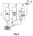
- Fig. 9 is a block diagram showing a demodulating circuit according to a fifth embodiment of the present invention.
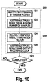
- Fig. 10 is a flowchart showing the operation of the demodulating circuit of the fifth embodiment of the invention.
- the demodulating circuit shown in Fig. 9 comprises a phase estimating circuit according to the first embodiment.
- reference numeral 33 denotes an inverse modulating circuit, which comprises a multiplier 15, a multiplier 16, and an adder 17.
- the multipliers 15, 16 multiply the output from an averaging filter 32 by the twiddle factor.
- the adder 17 adds the outputs from the multipliers 15, 16.
- Reference numeral 53 denotes an output terminal for outputting from the adder 17.
- Reference numeral 40 denotes a flip-flop for determining demodulation data in view of the input signal according to a recovered clock.
- phase estimating circuit comprises an input terminal 1, a signal generating circuit 9, a DFT circuit 31 and the averaging filter 32.
- the DFT circuit 31 determines DFT in view of an input signal and a twiddle factor from the signal generating circuit 9 (step 101 in Fig. 10), and the averaging filter 32 outputs phase information (step 102 in Fig. 10).
- the inverse modulating circuit 33 generates a recovered clock in view of the phase information (steps 107, 108 in Fig. 10).
- the recovered clock is prepared by inverse modulation (multiplying the determined phase information by the twiddle factor).
- the multiplier 15 and the multiplier 16 multiply the twiddle factor and the phase information output from the averaging filter 32 (step 107 in Fig. 10), and the multiplied results are added by the adder 15 (step 108 in Fig. 10).
- the output from the adder results from alternately selecting the output from the multiplier 15 and that from the multiplier 16 and adding a code of the input signal in conformity with a code of the twiddle factor. Therefore, if the averaging filter's output is given by the expression (16), a recovered clock is defined by the following expression (26). ⁇ 2S, 2S, -2S, -2S ⁇
- the flip-flop 40 reproduces and outputs demodulation data.
- phase estimating circuit of the first embodiment was described with reference to the phase estimating circuit of the first embodiment.
- the same demodulating circuit can be configured by the phase estimating circuits of the second to fourth embodiments based on the phase information output.
- Fig. 11 shows an embodiment in which a demodulating circuit is configured using the phase estimating circuits of the first to fourth embodiments and their estimating circuits are controlled by software.
- a phase estimating circuit comprises a signal generating circuit 9, a DFT circuit 31 and an averaging filter 32.
- the phase estimating circuit determines phase information of an input signal entered from an input terminal 1 and decimates data on the input signal based on the determined phase information to output demodulation data.
- phase estimating circuit of the first embodiment references the phase estimating circuit of the first embodiment, the same demodulating circuit can be configured using the phase estimating circuits of any one of the second to fourth embodiments based on the phase information output.
- the demodulating circuit can be configured using only software if phase information corresponding to demodulating data is available. Because a recovered clock can be omitted, the demodulating circuit can be simplified as shown in the block diagram of Fig. 11.
- the first aspect of the invention performs filtering of the result obtained by the discrete Fourier transform performed on a symbol basis, so that the accuracy of phase estimation is improved as compared with a conventional method.
- the second aspect of the invention stops the operation of the averaging filter if a clock component is not many as a result of the discrete Fourier transform performed on an input signal on a symbol basis, so that energy of the averaging filter can be prevented from lowering, and an effect of noises can be suppressed.
- the accuracy of phase estimation can be improved.
- the third aspect of the invention compares the output resulting from the discrete Fourier transform of an input signal performed on a symbol basis with the phase information output from the averaging filter and halts the operation of the averaging filter based on the compared result.
- the accuracy of phase estimation is improved.
- the fourth aspect of the invention monitors the energy of the averaging filter and stops the operation of the averaging filter based on the result of the pattern detection and that of the energy monitoring, so that the accuracy of phase estimation is improved.
- the fifth aspect of the invention can recover a recovered clock by the inverse modulation of phase information from the phase estimating circuit to obtain demodulation data of an input signal.
- the sixth aspect of the invention can decimate an input signal based on the phase information from the phase estimating circuit to obtain demodulation data of the input signal.
Landscapes
- Engineering & Computer Science (AREA)
- Computer Networks & Wireless Communication (AREA)
- Signal Processing (AREA)
- Synchronisation In Digital Transmission Systems (AREA)
- Digital Transmission Methods That Use Modulated Carrier Waves (AREA)
- Measuring Phase Differences (AREA)
Abstract
Description
{Y1(n), -Y2(n+1), -Y1(n+2), Y2(n+3), Y1(n+4), -Y2(n+5), ···}.
Claims (6)
- A phase estimating circuit for determining a phase component of a clock of an input signal, comprising:a signal generating circuit for generating a signal of a twiddle factor for discrete Fourier transform of cos and -sin components;a DFT circuit for performing the discrete Fourier transform for a predetermined number of symbols using the signal of the twiddle factor for the discrete Fourier transform and outputting the transformed result; andan averaging filter for averaging the results of the discrete Fourier transform output from the DFT circuit in order to output the averaged phase information.
- The phase estimating circuit according to claim 1, further comprising a pattern detecting circuit, which stops the operation of the averaging filter when the result of the discrete Fourier transform output from the DFT circuit includes a predetermined pattern.
- The phase estimating circuit according to claim 2, further comprising a phase detecting circuit, which determines a phase of the clock component of the input signal up to the previous symbol in view of the output from the averaging filter, outputs the obtained result as phase information to the pattern detecting circuit, and halts the operation of the averaging filter according to the result of the discrete Fourier transform performed by the DFT circuit and the phase information from the phase detecting circuit.
- The phase estimating circuit according to claim 2, further comprising an energy monitor, which determines energy of the clock component in view of the output from the averaging filter, compares the determined energy with a predetermined threshold, and outputs the compared result, and wherein:
the pattern detecting circuit halts the operation of the averaging filter according to the output resulting from the discrete Fourier transform performed by the DFT circuit and the output from the energy monitor. - A demodulating circuit, comprising the phase estimating circuit described in any one of claims 1 through 4, an inverse modulating circuit which generates a recovered clock based on phase information output from the phase estimating circuit and a twiddle factor for the discrete Fourier transform outputted from the signal generating circuit, and a decision circuit which judges the input signal for data using the recovered clock.
- A demodulating circuit, comprising the phase estimating circuit described in any one of claims 1 through 4 and a decimation circuit, which decimates data of the input signal based on phase information output from the phase estimating circuit and outputs demodulation data.
Applications Claiming Priority (3)
| Application Number | Priority Date | Filing Date | Title |
|---|---|---|---|
| JP25564797A JP3186665B2 (en) | 1997-09-19 | 1997-09-19 | Phase estimation circuit and demodulation circuit |
| JP255647/97 | 1997-09-19 | ||
| JP25564797 | 1997-09-19 |
Publications (3)
| Publication Number | Publication Date |
|---|---|
| EP0903884A2 true EP0903884A2 (en) | 1999-03-24 |
| EP0903884A3 EP0903884A3 (en) | 2002-09-25 |
| EP0903884B1 EP0903884B1 (en) | 2004-03-17 |
Family
ID=17281665
Family Applications (1)
| Application Number | Title | Priority Date | Filing Date |
|---|---|---|---|
| EP98111262A Expired - Lifetime EP0903884B1 (en) | 1997-09-19 | 1998-06-18 | Phase estimating circuit and demodulating circuit |
Country Status (7)
| Country | Link |
|---|---|
| US (1) | US5977820A (en) |
| EP (1) | EP0903884B1 (en) |
| JP (1) | JP3186665B2 (en) |
| CN (1) | CN1143492C (en) |
| AU (1) | AU708424B2 (en) |
| DE (1) | DE69822391T2 (en) |
| SG (1) | SG71127A1 (en) |
Families Citing this family (5)
| Publication number | Priority date | Publication date | Assignee | Title |
|---|---|---|---|---|
| US6914425B2 (en) * | 2003-04-29 | 2005-07-05 | Teradyne, Inc. | Measurement circuit with improved accuracy |
| JP4602170B2 (en) * | 2005-06-21 | 2010-12-22 | 三菱電機株式会社 | Clock recovery circuit and clock recovery method |
| US7606498B1 (en) * | 2005-10-21 | 2009-10-20 | Nortel Networks Limited | Carrier recovery in a coherent optical receiver |
| WO2011022869A1 (en) * | 2009-08-24 | 2011-03-03 | Huawei Technologies Co., Ltd. | Clock recovery apparatus |
| EP2922262B1 (en) * | 2014-03-17 | 2016-08-31 | The Swatch Group Research and Development Ltd. | Electronic circuit with synchronous demodulator of a phase-modulated signal |
Family Cites Families (6)
| Publication number | Priority date | Publication date | Assignee | Title |
|---|---|---|---|---|
| US3898446A (en) * | 1974-09-06 | 1975-08-05 | Us Army | Quadratic phase memory |
| FR2658017B1 (en) * | 1990-02-06 | 1992-06-05 | France Etat | METHOD FOR BROADCASTING DIGITAL DATA, ESPECIALLY FOR BROADBAND BROADCASTING TO MOBILES, WITH TIME-FREQUENCY INTERLACING AND ASSISTING THE ACQUISITION OF AUTOMATIC FREQUENCY CONTROL, AND CORRESPONDING RECEIVER. |
| JP3003826B2 (en) * | 1992-12-11 | 2000-01-31 | 三菱電機株式会社 | Clock recovery circuit |
| DE69434174T2 (en) * | 1994-12-22 | 2005-06-02 | Alcatel | Processor for carrier recovery |
| ATE233451T1 (en) * | 1996-09-02 | 2003-03-15 | St Microelectronics Nv | IMPROVEMENTS IN, OR RELATING TO, MULTI CARRIER TRANSMISSION SYSTEMS |
| US5870438A (en) * | 1996-09-26 | 1999-02-09 | Rockwell Int'l. Corp. | Fast resynchronization system for high-speed data transmission |
-
1997
- 1997-09-19 JP JP25564797A patent/JP3186665B2/en not_active Expired - Lifetime
-
1998
- 1998-03-25 US US09/047,416 patent/US5977820A/en not_active Expired - Fee Related
- 1998-04-30 CN CNB981087515A patent/CN1143492C/en not_active Expired - Fee Related
- 1998-06-15 AU AU71881/98A patent/AU708424B2/en not_active Ceased
- 1998-06-16 SG SG1998001431A patent/SG71127A1/en unknown
- 1998-06-18 DE DE69822391T patent/DE69822391T2/en not_active Expired - Fee Related
- 1998-06-18 EP EP98111262A patent/EP0903884B1/en not_active Expired - Lifetime
Also Published As
| Publication number | Publication date |
|---|---|
| JPH1198209A (en) | 1999-04-09 |
| SG71127A1 (en) | 2000-03-21 |
| JP3186665B2 (en) | 2001-07-11 |
| DE69822391D1 (en) | 2004-04-22 |
| US5977820A (en) | 1999-11-02 |
| EP0903884B1 (en) | 2004-03-17 |
| CN1143492C (en) | 2004-03-24 |
| CN1212547A (en) | 1999-03-31 |
| AU708424B2 (en) | 1999-08-05 |
| EP0903884A3 (en) | 2002-09-25 |
| AU7188198A (en) | 1999-04-15 |
| DE69822391T2 (en) | 2005-03-24 |
Similar Documents
| Publication | Publication Date | Title |
|---|---|---|
| EP1158739B1 (en) | Timing reproducer and demodulator comprising the same | |
| EP1168744A1 (en) | Timing reproducing device and demodulator | |
| JP4975085B2 (en) | Receiving apparatus and method | |
| KR960003194A (en) | Spread Spectrum Asynchronous Digital Receiver | |
| EP3621259B1 (en) | Method and device for fsk/gfsk demodulation | |
| US5694440A (en) | Data synchronizer lock detector and method of operation thereof | |
| US6192089B1 (en) | Electronic circuit and method for automatic frequency control | |
| EP0903884B1 (en) | Phase estimating circuit and demodulating circuit | |
| US6748030B2 (en) | Differential phase demodulator incorporating 4th order coherent phase tracking | |
| US5974100A (en) | Method and apparatus in a communication receiver for compensating for channel amplitude and phase distortion | |
| KR100335696B1 (en) | Device for communication system and method of using communication system | |
| US5307380A (en) | Delaying detection circuit | |
| EP1693954B1 (en) | Demodulation circuit for use in receiver using IF sampling scheme | |
| KR100325690B1 (en) | Apparatus and Method of Decision-Directed Carrier Recovery Based On LMS Method | |
| US20020141521A1 (en) | Receiver for a mobile radio terminal | |
| US5953385A (en) | Method and device for detecting the error on the frequency of a carrier | |
| JP3641469B2 (en) | Modulated carrier frequency detection method and apparatus | |
| US6560304B1 (en) | Apparatus for reducing pattern jitter by using locally symmetry forcing wave generating unit and method using the same | |
| JP2001177587A (en) | Digital modulation / demodulation synchronization method | |
| US7474147B2 (en) | Frequency shift keying signal demodulator method and apparatus | |
| US20070165703A1 (en) | Method and apparatus for robust automatic frequency control in cdma systems with constant pilot signals | |
| EP0633669B1 (en) | Method and apparatus for the detection of transmitted data in an electrical power distribution network | |
| JP3141927B2 (en) | Digital delay detection circuit | |
| US7804916B2 (en) | Detector for detecting a frequency-shift keying signal by digital processing | |
| GB2435383A (en) | Multilevel QAM symbol timing detecting circuit and multilevel QAM communication signal receiver |
Legal Events
| Date | Code | Title | Description |
|---|---|---|---|
| PUAI | Public reference made under article 153(3) epc to a published international application that has entered the european phase |
Free format text: ORIGINAL CODE: 0009012 |
|
| AK | Designated contracting states |
Kind code of ref document: A2 Designated state(s): AT BE CH CY DE DK ES FI FR GB GR IE IT LI LU MC NL PT SE |
|
| AX | Request for extension of the european patent |
Free format text: AL;LT;LV;MK;RO;SI |
|
| PUAL | Search report despatched |
Free format text: ORIGINAL CODE: 0009013 |
|
| AK | Designated contracting states |
Kind code of ref document: A3 Designated state(s): AT BE CH CY DE DK ES FI FR GB GR IE IT LI LU MC NL PT SE |
|
| AX | Request for extension of the european patent |
Free format text: AL;LT;LV;MK;RO;SI |
|
| 17P | Request for examination filed |
Effective date: 20021010 |
|
| 17Q | First examination report despatched |
Effective date: 20030224 |
|
| AKX | Designation fees paid |
Designated state(s): DE FR IT |
|
| GRAP | Despatch of communication of intention to grant a patent |
Free format text: ORIGINAL CODE: EPIDOSNIGR1 |
|
| GRAS | Grant fee paid |
Free format text: ORIGINAL CODE: EPIDOSNIGR3 |
|
| GRAA | (expected) grant |
Free format text: ORIGINAL CODE: 0009210 |
|
| AK | Designated contracting states |
Kind code of ref document: B1 Designated state(s): DE FR IT |
|
| REG | Reference to a national code |
Ref country code: IE Ref legal event code: FG4D |
|
| REF | Corresponds to: |
Ref document number: 69822391 Country of ref document: DE Date of ref document: 20040422 Kind code of ref document: P |
|
| ET | Fr: translation filed | ||
| PLBE | No opposition filed within time limit |
Free format text: ORIGINAL CODE: 0009261 |
|
| STAA | Information on the status of an ep patent application or granted ep patent |
Free format text: STATUS: NO OPPOSITION FILED WITHIN TIME LIMIT |
|
| 26N | No opposition filed |
Effective date: 20041220 |
|
| REG | Reference to a national code |
Ref country code: IE Ref legal event code: MM4A |
|
| PGFP | Annual fee paid to national office [announced via postgrant information from national office to epo] |
Ref country code: IT Payment date: 20080626 Year of fee payment: 11 |
|
| PGFP | Annual fee paid to national office [announced via postgrant information from national office to epo] |
Ref country code: DE Payment date: 20080626 Year of fee payment: 11 |
|
| PGFP | Annual fee paid to national office [announced via postgrant information from national office to epo] |
Ref country code: FR Payment date: 20080617 Year of fee payment: 11 |
|
| REG | Reference to a national code |
Ref country code: FR Ref legal event code: ST Effective date: 20100226 |
|
| PG25 | Lapsed in a contracting state [announced via postgrant information from national office to epo] |
Ref country code: FR Free format text: LAPSE BECAUSE OF NON-PAYMENT OF DUE FEES Effective date: 20090630 |
|
| PG25 | Lapsed in a contracting state [announced via postgrant information from national office to epo] |
Ref country code: DE Free format text: LAPSE BECAUSE OF NON-PAYMENT OF DUE FEES Effective date: 20100101 |
|
| PG25 | Lapsed in a contracting state [announced via postgrant information from national office to epo] |
Ref country code: IT Free format text: LAPSE BECAUSE OF NON-PAYMENT OF DUE FEES Effective date: 20090618 |