EP0903830B1 - Charging device for batteries in a mobile electrical unit - Google Patents
Charging device for batteries in a mobile electrical unit Download PDFInfo
- Publication number
- EP0903830B1 EP0903830B1 EP98117451A EP98117451A EP0903830B1 EP 0903830 B1 EP0903830 B1 EP 0903830B1 EP 98117451 A EP98117451 A EP 98117451A EP 98117451 A EP98117451 A EP 98117451A EP 0903830 B1 EP0903830 B1 EP 0903830B1
- Authority
- EP
- European Patent Office
- Prior art keywords
- push
- pull
- charging
- switches
- magnetic field
- Prior art date
- Legal status (The legal status is an assumption and is not a legal conclusion. Google has not performed a legal analysis and makes no representation as to the accuracy of the status listed.)
- Expired - Lifetime
Links
- 238000004804 winding Methods 0.000 claims abstract description 60
- 238000010168 coupling process Methods 0.000 claims description 10
- 238000005859 coupling reaction Methods 0.000 claims description 10
- 230000008878 coupling Effects 0.000 claims description 9
- 230000005540 biological transmission Effects 0.000 description 8
- 239000003990 capacitor Substances 0.000 description 8
- 230000001939 inductive effect Effects 0.000 description 6
- 230000010355 oscillation Effects 0.000 description 4
- 229910000859 α-Fe Inorganic materials 0.000 description 4
- 230000008901 benefit Effects 0.000 description 3
- 230000000903 blocking effect Effects 0.000 description 3
- 238000013461 design Methods 0.000 description 3
- 230000003071 parasitic effect Effects 0.000 description 3
- 230000001276 controlling effect Effects 0.000 description 2
- 230000004907 flux Effects 0.000 description 2
- 238000000034 method Methods 0.000 description 2
- 230000008569 process Effects 0.000 description 2
- 230000001681 protective effect Effects 0.000 description 2
- 230000001960 triggered effect Effects 0.000 description 2
- 238000013459 approach Methods 0.000 description 1
- 230000000740 bleeding effect Effects 0.000 description 1
- 230000008859 change Effects 0.000 description 1
- 238000006243 chemical reaction Methods 0.000 description 1
- 230000007423 decrease Effects 0.000 description 1
- 238000001514 detection method Methods 0.000 description 1
- 238000011161 development Methods 0.000 description 1
- 230000000694 effects Effects 0.000 description 1
- 230000005674 electromagnetic induction Effects 0.000 description 1
- 238000005265 energy consumption Methods 0.000 description 1
- 238000005516 engineering process Methods 0.000 description 1
- 230000002708 enhancing effect Effects 0.000 description 1
- 230000002349 favourable effect Effects 0.000 description 1
- 230000017525 heat dissipation Effects 0.000 description 1
- 238000010438 heat treatment Methods 0.000 description 1
- 230000006698 induction Effects 0.000 description 1
- 230000003287 optical effect Effects 0.000 description 1
- 230000000737 periodic effect Effects 0.000 description 1
- 230000002265 prevention Effects 0.000 description 1
- 230000009467 reduction Effects 0.000 description 1
- 230000001105 regulatory effect Effects 0.000 description 1
- 238000000926 separation method Methods 0.000 description 1
- 230000001629 suppression Effects 0.000 description 1
- 238000012360 testing method Methods 0.000 description 1
Images


Classifications
-
- H—ELECTRICITY
- H02—GENERATION; CONVERSION OR DISTRIBUTION OF ELECTRIC POWER
- H02J—CIRCUIT ARRANGEMENTS OR SYSTEMS FOR SUPPLYING OR DISTRIBUTING ELECTRIC POWER; SYSTEMS FOR STORING ELECTRIC ENERGY
- H02J50/00—Circuit arrangements or systems for wireless supply or distribution of electric power
- H02J50/10—Circuit arrangements or systems for wireless supply or distribution of electric power using inductive coupling
- H02J50/12—Circuit arrangements or systems for wireless supply or distribution of electric power using inductive coupling of the resonant type
-
- H—ELECTRICITY
- H02—GENERATION; CONVERSION OR DISTRIBUTION OF ELECTRIC POWER
- H02J—CIRCUIT ARRANGEMENTS OR SYSTEMS FOR SUPPLYING OR DISTRIBUTING ELECTRIC POWER; SYSTEMS FOR STORING ELECTRIC ENERGY
- H02J50/00—Circuit arrangements or systems for wireless supply or distribution of electric power
- H02J50/60—Circuit arrangements or systems for wireless supply or distribution of electric power responsive to the presence of foreign objects, e.g. detection of living beings
-
- H—ELECTRICITY
- H02—GENERATION; CONVERSION OR DISTRIBUTION OF ELECTRIC POWER
- H02J—CIRCUIT ARRANGEMENTS OR SYSTEMS FOR SUPPLYING OR DISTRIBUTING ELECTRIC POWER; SYSTEMS FOR STORING ELECTRIC ENERGY
- H02J7/00—Circuit arrangements for charging or depolarising batteries or for supplying loads from batteries
- H02J7/0029—Circuit arrangements for charging or depolarising batteries or for supplying loads from batteries with safety or protection devices or circuits
- H02J7/00308—Overvoltage protection
Definitions
- the invention relates to a charging device for charging batteries in a mobile electrical unit, for example a radiotelephone, a cordless telephone, or the like, in which the energy is inductively transmitted from a charging unit to the mobile unit coupled by a alternating magnetic field.
- the charging device detects when no energy for charging is being drawn on the secondary side or when in lieu of the mobile electrical unit, a foreign body is drawing energy from the alternating magnetic field and then switches automatically back into a low-power standby mode.
- the charging energy must be as lossfree as possible and must be conveyed to the battery with a minimum of control means in the phone device, i.e. the charging unit must at least have a current limitation.
- the mobile unit is advantageously intended to be coupled to the charging unit without electrical contacts.
- the device For a continuous reachability by incoming calls, the device must additionally be ready to receive even during charging.
- the charging unit is not permitted to influence the function of the connected mobile radio device, as is possible, for example, due to electromagnetically radiated interference from the harmonic waves of the switching pulses and can only be prevented in conventional switching converters by means of costly filters and shields.
- the resonance converter uses a push-pull oscillator, two switches periodically connect this oscillating circuit, to input DC voltage so that a recharging occurs periodically between the circuit capacitance and primary part.
- the resonance frequency depends not only on the inductance of the primary winding of the transformer and the circuit capacitance, but also on the secondary load.
- the resonance frequency increases in a resonance converters. Consequently, the resonance frequency coincides with the supplied control frequency only in a narrow load range. If the resonance converter functions outside this range, either the resonance current breaks off prematurely or the switches are heavily loaded as a result of the incorrect trigger timing. Also heavy energy losses can occur when switching over if both of the control electrodes of the switches are temporarily conductive, for example as a result of parasitic storage capacitances.
- additional control means and/or protective measures such as protective diodes are required. The latter lead to additional energy losses and increase the interference emission in the high frequency range.
- the reference EP 0 293 874 B1 has disclosed a process and a circuit arrangement for status control for an oscillating circuit in a resonance converter.
- a costly control circuit monitors the current and/or voltage behavior in the resonance circuit by means of an inductive current-voltage converter disposed in series in relation to the primary winding and generates a triggering frequency for the switches, which is continuously modulated to the changing natural frequency.
- the resonance condition is maintained over a large load range.
- the references EP 0 589 911 B1 and EP 0 589 912 B1 have disclosed switch regulators which contain a resonance converter with a push-pull oscillator, which is powered by a pre-regulator that is scanned with a pulse-width modulated signal.
- the pre-regulator decreases an intensely fluctuating input voltage and contains two individual inductances for uncoupling the feed of the input currents into the push-pull branches.
- the two primary windings of a push-pull transmitter that are galvanically separated from each other each constitute a secondary-side resonance circuit.
- the circuit capacitances respectively apply regulated operating currents to the inputs for the current feed and have DC potential.
- Two switches alternatingly switch the primary windings of the push-pull branches in relation to ground. Between the switch changes, both of the switches are without current during a so-called gap time.
- the gap time should permit an oscillation of the push-pull converter including parasitic winding capacitances or capacitances rectifiers that are not explained in detail.
- a control device clearly excites the switches independent of the load. The voltages that are present at the circuit capacitances and are added in a summing network, and the input current of the pre-regulator are used as control criteria for the pulse-width modulation. The input current of the pre-regulator is detected by an inductive current converter.
- Inductive charging devices for mobile radiotelephones have also been disclosed.
- the reference GB 2291 291A has disclosed a non-contacting battery charging device for supplying electric power from a charger without direct contact to an accumulator battery in a radio telephone.
- a charging unit comprises a primary coil, an oscillator for supplying AC power to the coil and an oscillator control section connected with means for turning on and off the power supplied to the oscillator.
- the radiotelephone contains circuits for generating a halt signal that halts the supply of AC power to the oscillator automatically via an optical link by an incoming call or by operating keys of the telephone keyboard. That eliminates the attractive force caused by electromagnetic induction between the radiotelephone and the charger to enable easy removal of the telephone from the charger.
- a contact switch arranged in a depression of the charger turns the charger on when the radiotelephone is placed within the charger.
- the reference US-A-5 428 521 discloses a charging unit that inductively transmits electrical power by means of an alternating magnetic field from at least one primary winding to at least secondary winding in a mobile unit.
- the alternating magnetic field is generated by a self-oscillating push-pull oscillator that contains switches.
- Charging devices of the prior art transmit only a low electrical charging power to the radiotelephone, which is insufficient for quick charges, although the devices contain voluminous primary and secondary windings.
- these known charging devices have a high-energy consumption and an intense magnetic interference emission in relation to the power transmitted.
- the operating mode of a charging device with high power transmission creates a great problem for operational reliability, when the device does not switch into a low-power standby mode automatically.
- the charging unit in the no-load state, i.e. when a charging control in the mobile unit has ended the charging process, or when the mobile unit has been removed from the charging unit, the charging unit requires a considerable amount of power so that in continuous operation, additional measures are necessary for a continuously reliable bleeding off of power.
- foreign bodies that are electrically and/or magnetically conductive and get into the alternating field by chance, for example coins, metallic office accessories and the like, can absorb a lot of energy from the alternating field, heat up intensely due to inductively generated short circuit currents and eddy currents, and represent a danger for the surrounding area.
- Known resonance converters have expensive control circuits with additional inductive components in order to precisely control the switches in the load range from no-load to full-load. Furthermore, the known resonance converters are only insufficiently equipped with control means that permit a primary-side detection of and reaction to changes in the load by means of the secondary, e.g. the removal of the mobile unit after the charging of the batteries is finished.
- the invention provides a device for charging batteries according to claim 1 and a mobile unit according to claim 11.
- the object of the invention is to produce a charging device of the type described before, with an extremely compact design, in which a DC converter that is constructed with simple means has minimal energy losses and minimal electromagnetic interference emission in a load range from no-load to full-load. Furthermore, in the event of no-load operation or when a foreign body influences the magnetic field, the charging unit should switch back into a low-power standby mode.
- the invention is based on a charging device in which a charging unit transmits power to a mobile unit using a alternating magnetic field.
- the alternating magnetic field is generated by the primary windings of a self-oscillating push-pull oscillator with separate resonance circuits in each push-pull branch. Switches are disposed in the push-pull branches, which are triggered by way of a positive feedback from the opposite push-pull branch.
- each resonance circuit contains the inductance of a primary winding W1 or W2, which when a mobile unit MU is brought close, is coupled with a coupling factor k to the respectively opposite secondary winding W3 or W4, wherein preferably, the equation 0.2 ⁇ k ⁇ 0.6 applies.
- the primary windings in the charging unit are in fact connected to a common core, but are disposed spatially separate from each other so that each generates a alternating magnetic field in a different spatial region, which can be separately influenced.
- a self-oscillating converter has the advantage that the timing of the switches is precisely determined by the momentary frequency value of the primary resonance circuits without expensive control means.
- the oscillation circuits of the push-pull branches react independently of each other to unequal loads of the spatial regions of the magnetic alternating field.
- electrical operating values are present that are different in the push-pull branches, depending on the load.
- these values are the voltage by way of the switches and the operating current of each push-pull branch.
- the load types in the secondary part of the alternating magnetic field such as full-load, no-load, and incorrect load due to a foreign body, can be detected in the charging unit and corresponding measures can be automatically triggered, such as the reduction or the switching off of the energy supply.
- FIG. 1 shows a charging unit CU for charging an accumulator battery B in a mobile electrical unit MU, which in the current example is a mobile telephone.
- a power supply PS supplies an input DC voltage U IN for a push-pull oscillator with each series circuit comprised of a primary winding W1 or W2 and switches Q1 and Q2 in the push-pull branches.
- a control circuit SC which on the one hand, evaluates the voltages U D1 , U D2 by way of the switches Q1, Q2 and on the other hand, evaluates voltage drops at impedances R1, R2 in each of the push-pull branches depending on operating current I IN , generates a control voltage U C for a control input terminal CIN of the power supply PS.
- the power supply PS is a conventional AC/DC switching converter, which converts the public network voltage AC into an input DC voltage U IN and has an control input terminal CIN for switching off the input DC voltage U IN .
- the input CIN is advantageously disposed in a conventional circuit for controlling the switching converter.
- the charging unit CU is provided for use in a motor vehicle, then the AC/DC switching converter is replaced by a simple electronic on/off switch for interrupting the operating current supply.
- control voltage Uc can also be used for muting the push-pull oscillator.
- the primary windings W1, W2 generate the alternating magnetic field required for the energy transmission and are advantageously connected to the arm ends of a U-shaped ferrite core F1, which is disposed close beneath the surface of the housing of the charging unit CU.
- the secondary side circuitry in the mobile unit MU represented on fig. 1 and described herebelow is given as illustrative example not being part of the invention.
- a secondary winding W3 or W4 is contained in the housing of the mobile unit MU, and in the example, these secondary windings W3, W4 are disposed parallel to an additional circuit capacitance C8 and with it, form a secondary resonance circuit.
- the resonance frequency of the resonance circuit C8, W3, W4 should be close to the oscillating frequency of the push-pull oscillator.
- the secondary-side resonance has only a slight influence on the power transmission.
- the secondary windings W3, W4, analogous to the primary windings W1, W2, are advantageously disposed on the arm ends of a second U-shaped ferrite core F2, which is disposed close beneath the surface of the housing of the mobile unit MU. It is important for the function of the charging device that the secondary windings W3, W4 evenly load the primary windings W1, W2.
- An average coupling factor k of up to approximately 0.40, together with the data of the resonance circuit C8, W3, W4, permits a favorable secondary-side current limitation so that no power has to be converted for this in the mobile unit MU.
- the housing of the charging unit CU has a mechanical guide FK and/or mount, which is adapted to the shape of the mobile unit MU.
- the arrangement of windings on the arm ends of U-shaped ferrite cores F1, F2 on the one hand has the advantage that for the effective power transmission, the rear magnetic fluxes of the primary windings W1, W2 and the secondary windings W3, W4 are closed.
- the U-shaped ferrite cores make an extremely flat design of a mobile telephone possible.
- the local separation of the primary windings W1, W2 requires that only a mobile unit MU, which has a corresponding resonance circuit C8, W3, W4 with secondary windings W3, W4 in the same arrangement as the charging unit CU, can draw the full energy quantity from the alternating field.
- the resonance conditions of the circuits in the push-pull branches change on the secondary side, which has an influence on the voltage by way of the switches and the operating current of each push-pull branch.
- the coupling of the load to the secondary-side resonance circuit C8, W3, W4 is carried out by way of a charging rectifier D3, in this case a bridge rectifier.
- this charging rectifier D3 supplies the charging output voltage U OUT for the accumulator battery B.
- a charging control circuit CC can be connected between the charging rectifier D3 and the accumulator battery B, and this control circuit CC interrupts the power supply to the accumulator battery B when it is fully charged. In this way, the push-pull oscillator is switched from full-load operation into no-load operation even without removal of the mobile unit MU.
- the circuitry of the DC converter is based on an intrinsically known self-oscillating push-pull oscillator, in which in the current example, the switches Q1, Q2 are connected with positive feedback by way of capacitive voltage dividers C1, C3 or C2, C4 from the opposite push-pull branch.
- FIG. 2a shows the circuit of the push-pull oscillator according to the invention.
- the positive feedback can also occur inductively, for example by means of a coupling winding being attached to each of the arm ends of the opposite push-pull branch.
- the push-pull oscillator used in the invention contains two separate series oscillating circuits W1, C1, C3 and W2, C2, C4 disposed parallel to the input DC voltage U IN .
- the circuit capacitances of the push-pull branches are each embodied as capacitive voltage dividers or C2, C4, and are disposed parallel to the switch Q1 or Q2.
- the circuit inductance is disposed in series with this, and, due to the large air gap, is predominantly constituted by the inductance of the primary winding W1 or W2.
- the impedances R1 and R2, which advantageously are ohmic resistances with resistance values of up to several ohms, are disposed in series to the primary winding W1 or W2, in the present case at the input DC voltage U IN .
- these ohmic resistances are connected to the capacitors C5 and C6, whose capacitance is much larger than the effective capacitance of the capacitive voltage divider C1, C3, or C2, C4 and these capacitors therefore have only a very slight influence on the resonance behavior of the primary resonance circuits.
- the switches Q1, Q2 are MOSFETs of the enhancement type, which require a gate-source threshold voltage of approximately 4V in order to switch on.
- the operating points in the switches Q1, Q2 can be adjusted in a simple manner, namely by means of dimensioning the capacitive voltage dividers C1, C3 or C2, C4 and the resistances R3 to R6, so that after a switch is turned off, a voltage U D1 , U D2 must first be built up by the circuit inductance because of this turning off of the switch, before the opposite switch turns on.
- the second closes only if the voltage at the output of the capacitive voltage divider, by way of the first switch, exceeds the gate-source threshold voltage.
- each switch remains closed as long as the voltage at the output of the capacitive voltage divider from the other push-pull branch exceeds the gate-source threshold voltage. If, for example due to an increase in the load on the secondary side and the resultant increase in the resonance frequency, the recharging times are shortened at the open switch, then the other remains closed for a correspondingly shorter time. In this manner, even when there are uneven loads on the primary windings W1, W2, the switching times of the switches always remain exactly adjusted as a function of the load conditions.
- the resonance frequency is at its highest, since the influence from the secondary part of the magnetic circuit is not there.
- the resonance frequency is at its lowest when the mobile unit MU is coupled and the accumulator battery B is charged. When the accumulator battery B is not charged, the resonance frequency lies between these.
- the resistances R3 and R4 support a reliable oscillation of the oscillating circuit and can also be omitted in actual use, if the power supply PS has a low intrinsic impedance and when there is a corresponding dimensioning of the circuit components so that a rapid charging of the capacitive voltage divider C1, C3 or C2, C4 occurs.
- the self-oscillating push-pull oscillator in no way requires additional drivers for controlling the switches Q1, Q2 and the parasitic capacitances, in particular the relatively large gate-source capacitance of the switches Q1, Q2, are disposed parallel to the capacitors C1, C3 and C2, C4 of the circuit capacitances, these can be recharged without resistive losses in comparison to known embodiments in which a control is carried out by ohmic resistances.
- the push-pull oscillator therefore has only a very low internal loss and can easily transmit a high frequency power of several Watts with a switching frequency of over 500 kHz in order to charge the mobile unit MU.
- FIG. 2b shows the secondary-side circuitry in the mobile unit MU according to the invention.
- the secondary-side winding W3, W4 are connected in series.
- Each of the windings W3, W4 is disposed parallel to an own circuit capacitance C8.1 or C8.2 and forms a separate secondary resonance circuit.
- the resonance frequency of both resonance circuits C8.1, W3 and C8.2, W4 should be a little above to the oscillating frequency of the push-pull oscillator at least when the charger operates in full-load mode.
- Each resonance circuit C8.1, W3 or C8.2 W4 is connected separately with a charging rectifier diode D3.1 or D3.2 to create a known two-way rectification.
- the conducting directions of the charging rectifier diodes D3.1 and D3.2 are arranged in such a manner that only that rectifier diode D3.1 and D3.2 carries forward current I3 or I4 momentary via the corresponding secondary winding W3 or W4 which is arranged opposite to that primary winding W1 or W2 that has left the conducting state a short period before. That means for instance, when switch Q1 is switched on and primary winding W1 carries switching current I 1 than rectifier diode D3.1 is blocked. But when switch Q 1 blocks, the energy of the magnetic field is transformed into electric energy and charges the primary circuit capacitances C1, C3 and the secondary circuit capacitance C8.1.
- the embodiment according FIG. 2b causes an enhancing of efficiency of power transmission to the mobile unit MU and a better stability of the output voltage depending on the secondary load.
- the solution shows the best transmission efficiency when the resonance frequency of both resonance circuits C8.1, W3 and C8.2, W4 is close to the oscillating frequency of the push-pull oscillator at least when the charger operates in full-load mode.
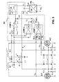
- FIG. 3 shows another particularly advantageous embodiment of the invention.
- the primary circuit of the resonance converter in the charging unit CU is connected to the control circuits SC.
- This control circuit is intended to detect from the load whether either the mobile unit MU is not coupled or the mobile unit MU is coupled and the accumulator battery B is charged or an uneven loading of the alternating magnetic field exists by means of foreign bodies. It is thereby assumed that foreign bodies generally influence the spatial regions of the primary windings W1, W2 unevenly.
- the surface of the charging unit CU can be correspondingly shaped to realize this. An uneven influence brings on the one hand, the duration of the recharging times at the respectively open switches Q1, Q2 out of equilibrium.
- the amplitudes of the voltages U D1 , U D2 at the open switches Q1, Q2 are unequal.
- differences in the power drawn from the primary resonance circuits also induce assessable deviations of the operating currents I1, I2 in the push-pull branches.
- the control circuit SC contains a comparator COMP 1 for comparing peak voltage values of the switching voltages U D1 , U D2 . Since the switching voltages U D1 , U D2 occur in the push-pull mode, a comparison is only possible if the level peaks are kept by peak value formers PV 1, PV 2 or similar storage devices.
- the comparator COMP 1 is a differential amplifier whose output circuit is embodied so that the comparison result always appears as an absolute value. This is achieved, for example, with a circuit shown in Fig. 4.
- the peak value formers PV 1, PV 2 contain charge capacitors that are charged by way of diodes D6, D7. As a result of the induction voltage, the peak values are above the input DC voltage U IN , at approximately 40V in the present example.
- the comparison is executed with the transistors Q 3, Q 4, which along with the emitter resistances R9, R10 and the joint collector resistance R11, constitute a differential amplifier which generates a DC voltage U A1 at the collector resistance R11 when there is an inequality of the peak values.
- the emitter resistances R9, R10 can be embodied as base voltage dividers with additional resistances that are depicted with dashed lines.
- the switch LA opens and the power supply PS switches the input DC voltage U IN back on. As a result, the push-pull oscillator begins to oscillate.
- the comparator COMP 1 once again generates an output voltage U A1 > 0 and the input CIN once again switches off the input DC voltage D IN after an interval T2.
- control circuit is dimensioned in such a way that T1 > T2, then a low-power standby mode can be realized using simple means.
- the control circuit SC has a comparator COMP 2 for evaluating differences in the power draw. As shown in Fig. 3, this measures the voltages that the operating currents I1, I2 of the push-pull branches produce across the impedances R1, R2 and is likewise a differential amplifier. The output circuit is also embodied so that the comparison result always appears as an absolute value.
- Fig. 5 shows a possible embodiment for the comparator. The circuitry is similar to that in Fig. 4. In contrast to the comparator COMP 1, in addition to the differential stage described, which has the transistors Q5, Q6 and the emitter resistances R14, R15, there is an additional differential amplifier stage A for adapting the comparator inputs to the voltages at the impedances R1, R2.
- the relatively high voltage at the peak value formers PV 1, PV 2 is averaged with resistances R12, R13 and a charging capacitor and is used by the comparator COMP 2 as an operating voltage for the differential stages Q5, Q6.
- the output from the comparator COMP 2 is connected to the collector resistance R11 like that of COMP 1.
- the signal adder ADD shown in Fig. 3 is realized.
- the signal adder ADD effects that the output voltage U A1 is a function of inequalities both of the switching voltages U D1 , U D2 and of the operating currents I1, I2.
Landscapes
- Engineering & Computer Science (AREA)
- Power Engineering (AREA)
- Computer Networks & Wireless Communication (AREA)
- Charge And Discharge Circuits For Batteries Or The Like (AREA)
Abstract
Description
- The invention relates to a charging device for charging batteries in a mobile electrical unit, for example a radiotelephone, a cordless telephone, or the like, in which the energy is inductively transmitted from a charging unit to the mobile unit coupled by a alternating magnetic field. The charging device detects when no energy for charging is being drawn on the secondary side or when in lieu of the mobile electrical unit, a foreign body is drawing energy from the alternating magnetic field and then switches automatically back into a low-power standby mode.
- The continuing development in the field of mobile radio technology has led to particularly compact and light mobile radiotelephone, so-called "mobile phones", and cordless telephones that are operated by batteries with high energy density. In the interests of a high degree of mobility and a continuous use, batteries of this kind must have a high capacitance and must be rechargeable in an extremely short time by means of public network energy or the on-board voltage of a vehicle. Since the batteries should also already have sufficient energy for the transmitting operation after a short charge time, an extremely light and compact charging unit is necessary, which for so-called quick charges supplies a relatively large amount of charging energy into the mobile unit. Due to the compactness of mobile radiotelephones, the charging energy must be as lossfree as possible and must be conveyed to the battery with a minimum of control means in the phone device, i.e. the charging unit must at least have a current limitation. In the interests of reliability and comfort, the mobile unit is advantageously intended to be coupled to the charging unit without electrical contacts. For a continuous reachability by incoming calls, the device must additionally be ready to receive even during charging. The charging unit is not permitted to influence the function of the connected mobile radio device, as is possible, for example, due to electromagnetically radiated interference from the harmonic waves of the switching pulses and can only be prevented in conventional switching converters by means of costly filters and shields.
- The requirements mentioned are fulfilled particularly well by charging units which contain a DC converter wired with L-C-resonance circuits, since these converters feature low interference emission in the high frequency range and a low power loss. In addition, in comparison to other switching converters, this special embodiment of switching converters, a so called resonance converter, does not cause any rapid current and voltage changes and can therefore be operated at higher switching frequencies. This makes it possible, that a transformer can be used for the resonance converter which is very low in volume and weight.
- In general, in resonance converters, at least the primary part of the transformer, together with a circuit capacitance, constitutes an oscillating circuit. In case when the resonance converter uses a push-pull oscillator, two switches periodically connect this oscillating circuit, to input DC voltage so that a recharging occurs periodically between the circuit capacitance and primary part.
- In resonance converters, however, there is a known problem in that the resonance frequency depends not only on the inductance of the primary winding of the transformer and the circuit capacitance, but also on the secondary load. With increasing secondary power consumption, the resonance frequency increases in a resonance converters. Consequently, the resonance frequency coincides with the supplied control frequency only in a narrow load range. If the resonance converter functions outside this range, either the resonance current breaks off prematurely or the switches are heavily loaded as a result of the incorrect trigger timing. Also heavy energy losses can occur when switching over if both of the control electrodes of the switches are temporarily conductive, for example as a result of parasitic storage capacitances. In order to prevent the disadvantages mentioned, additional control means and/or protective measures such as protective diodes are required. The latter lead to additional energy losses and increase the interference emission in the high frequency range.
- Various embodiments are known for the prevention of this disadvantage. For example, the reference EP 0 293 874 B1 has disclosed a process and a circuit arrangement for status control for an oscillating circuit in a resonance converter. A costly control circuit monitors the current and/or voltage behavior in the resonance circuit by means of an inductive current-voltage converter disposed in series in relation to the primary winding and generates a triggering frequency for the switches, which is continuously modulated to the changing natural frequency. The resonance condition is maintained over a large load range.
- The references EP 0 589 911 B1 and EP 0 589 912 B1 have disclosed switch regulators which contain a resonance converter with a push-pull oscillator, which is powered by a pre-regulator that is scanned with a pulse-width modulated signal. The pre-regulator decreases an intensely fluctuating input voltage and contains two individual inductances for uncoupling the feed of the input currents into the push-pull branches. With separate circuit capacitances, the two primary windings of a push-pull transmitter that are galvanically separated from each other each constitute a secondary-side resonance circuit. The circuit capacitances respectively apply regulated operating currents to the inputs for the current feed and have DC potential. Two switches alternatingly switch the primary windings of the push-pull branches in relation to ground. Between the switch changes, both of the switches are without current during a so-called gap time. In accordance with the description, the gap time should permit an oscillation of the push-pull converter including parasitic winding capacitances or capacitances rectifiers that are not explained in detail. A control device clearly excites the switches independent of the load. The voltages that are present at the circuit capacitances and are added in a summing network, and the input current of the pre-regulator are used as control criteria for the pulse-width modulation. The input current of the pre-regulator is detected by an inductive current converter.
- Inductive charging devices for mobile radiotelephones have also been disclosed. For example, the reference GB 2291 291A has disclosed a non-contacting battery charging device for supplying electric power from a charger without direct contact to an accumulator battery in a radio telephone. A charging unit comprises a primary coil, an oscillator for supplying AC power to the coil and an oscillator control section connected with means for turning on and off the power supplied to the oscillator. The radiotelephone contains circuits for generating a halt signal that halts the supply of AC power to the oscillator automatically via an optical link by an incoming call or by operating keys of the telephone keyboard. That eliminates the attractive force caused by electromagnetic induction between the radiotelephone and the charger to enable easy removal of the telephone from the charger. In an especially embodiment of the known solution a contact switch arranged in a depression of the charger turns the charger on when the radiotelephone is placed within the charger.
- The reference US-A-5 428 521 discloses a charging unit that inductively transmits electrical power by means of an alternating magnetic field from at least one primary winding to at least secondary winding in a mobile unit. The alternating magnetic field is generated by a self-oscillating push-pull oscillator that contains switches.
- Charging devices of the prior art transmit only a low electrical charging power to the radiotelephone, which is insufficient for quick charges, although the devices contain voluminous primary and secondary windings. In addition, these known charging devices have a high-energy consumption and an intense magnetic interference emission in relation to the power transmitted.
- The operating mode of a charging device with high power transmission creates a great problem for operational reliability, when the device does not switch into a low-power standby mode automatically.
- Also, in the no-load state, i.e. when a charging control in the mobile unit has ended the charging process, or when the mobile unit has been removed from the charging unit, the charging unit requires a considerable amount of power so that in continuous operation, additional measures are necessary for a continuously reliable bleeding off of power. Furthermore, foreign bodies that are electrically and/or magnetically conductive and get into the alternating field by chance, for example coins, metallic office accessories and the like, can absorb a lot of energy from the alternating field, heat up intensely due to inductively generated short circuit currents and eddy currents, and represent a danger for the surrounding area. Even a mobile telephone or another device that is not equipped for inductive energy transmission can inadvertently get into the region of the alternating field and possibly even get damaged due to a continuous inductive heating. On the other hand, by shifting the resonance condition, the foreign bodies can considerably increase the power consumption of the charging device so that it is destroyed when there is insufficient heat dissipation.
- Known resonance converters have expensive control circuits with additional inductive components in order to precisely control the switches in the load range from no-load to full-load. Furthermore, the known resonance converters are only insufficiently equipped with control means that permit a primary-side detection of and reaction to changes in the load by means of the secondary, e.g. the removal of the mobile unit after the charging of the batteries is finished.
- The invention provides a device for charging batteries according to
claim 1 and a mobile unit according toclaim 11. - The object of the invention is to produce a charging device of the type described before, with an extremely compact design, in which a DC converter that is constructed with simple means has minimal energy losses and minimal electromagnetic interference emission in a load range from no-load to full-load. Furthermore, in the event of no-load operation or when a foreign body influences the magnetic field, the charging unit should switch back into a low-power standby mode.
- In order to attain the object, the invention is based on a charging device in which a charging unit transmits power to a mobile unit using a alternating magnetic field. According to the invention, the alternating magnetic field is generated by the primary windings of a self-oscillating push-pull oscillator with separate resonance circuits in each push-pull branch. Switches are disposed in the push-pull branches, which are triggered by way of a positive feedback from the opposite push-pull branch.
- In addition to the circuit capacitance, each resonance circuit contains the inductance of a primary winding W1 or W2, which when a mobile unit MU is brought close, is coupled with a coupling factor k to the respectively opposite secondary winding W3 or W4, wherein preferably, the equation 0.2 ≤ k ≤ 0.6 applies. According to the invention, the primary windings in the charging unit are in fact connected to a common core, but are disposed spatially separate from each other so that each generates a alternating magnetic field in a different spatial region, which can be separately influenced.
A self-oscillating converter has the advantage that the timing of the switches is precisely determined by the momentary frequency value of the primary resonance circuits without expensive control means. - Caused by separate arranged primary windings, the oscillation circuits of the push-pull branches react independently of each other to unequal loads of the spatial regions of the magnetic alternating field. This has the advantage that in the circuit according to the invention, electrical operating values are present that are different in the push-pull branches, depending on the load. In particular, these values are the voltage by way of the switches and the operating current of each push-pull branch. In conjunction with these operating values, the load types in the secondary part of the alternating magnetic field, such as full-load, no-load, and incorrect load due to a foreign body, can be detected in the charging unit and corresponding measures can be automatically triggered, such as the reduction or the switching off of the energy supply.
- The invention is explained below in conjunction with an exemplary embodiment. In particular, the corresponding drawings show the following:
- FIG. 1
- shows the principle for transmitting charging power according to the invention from a charging unit to a mobile electrical unit,
- FIG. 2a
- shows the primary circuitry of the resonance converter in the charging unit,
- FIG. 2b
- shows a preferred embodiment of the secondary circuitry of the resonance converter in the mobile electrical unit,
- FIG. 3
- shows the primary circuitry of the resonance converter in the charging unit connected to a control circuit for detecting no-load operation and uneven loads of the alternating magnetic field,
- FIG. 4
- shows an exemplary embodiment for a first comparator for detecting uneven load of the primary resonance circuits in the charging unit,
- FIG. 5
- shows an exemplary embodiment for a second comparator for detecting an uneven load of the primary resonance circuits in the charging unit.
- FIG. 1 shows a charging unit CU for charging an accumulator battery B in a mobile electrical unit MU, which in the current example is a mobile telephone. In the charging unit CU, a power supply PS supplies an input DC voltage UIN for a push-pull oscillator with each series circuit comprised of a primary winding W1 or W2 and switches Q1 and Q2 in the push-pull branches. A control circuit SC, which on the one hand, evaluates the voltages UD1, UD2 by way of the switches Q1, Q2 and on the other hand, evaluates voltage drops at impedances R1, R2 in each of the push-pull branches depending on operating current IIN, generates a control voltage UC for a control input terminal CIN of the power supply PS.
- For a public network-operated charging unit CU, for example, the power supply PS is a conventional AC/DC switching converter, which converts the public network voltage AC into an input DC voltage UIN and has an control input terminal CIN for switching off the input DC voltage UIN. The input CIN is advantageously disposed in a conventional circuit for controlling the switching converter.
- If the charging unit CU is provided for use in a motor vehicle, then the AC/DC switching converter is replaced by a simple electronic on/off switch for interrupting the operating current supply.
- According to another embodiment of the invention, the control voltage Uc can also be used for muting the push-pull oscillator.
- The primary windings W1, W2 generate the alternating magnetic field required for the energy transmission and are advantageously connected to the arm ends of a U-shaped ferrite core F1, which is disposed close beneath the surface of the housing of the charging unit CU.
- The secondary side circuitry in the mobile unit MU represented on fig. 1 and described herebelow is given as illustrative example not being part of the invention.
- In addition to the conventional mobile telephone part RT and the accumulator battery B, for each push-pull branch, a secondary winding W3 or W4 is contained in the housing of the mobile unit MU, and in the example, these secondary windings W3, W4 are disposed parallel to an additional circuit capacitance C8 and with it, form a secondary resonance circuit. In the interests of a maximal energy transmission to the mobile unit MU, the resonance frequency of the resonance circuit C8, W3, W4 should be close to the oscillating frequency of the push-pull oscillator. As a result, when there is a high coupling factor k, the secondary-side resonance has only a slight influence on the power transmission. In this case, it is advantageous to optimize the circuit capacitance C8 with regard to the suppression of RF interferences that are produced at the rectifier D3.
- In the other case, it is advantageous for the avoidance of a high secondary no-load voltage, to select the value of the circuit capacitance C8 lower than is needed for the resonance condition. As a result, on the secondary side, on the one hand, a voltage limitation is produced at low load, while when there is high load and in the event of a short circuit, current limitation takes place in connection with the coupling mentioned.
- The secondary windings W3, W4, analogous to the primary windings W1, W2, are advantageously disposed on the arm ends of a second U-shaped ferrite core F2, which is disposed close beneath the surface of the housing of the mobile unit MU. It is important for the function of the charging device that the secondary windings W3, W4 evenly load the primary windings W1, W2. An average coupling factor k of up to approximately 0.40, together with the data of the resonance circuit C8, W3, W4, permits a favorable secondary-side current limitation so that no power has to be converted for this in the mobile unit MU.
- In order to enable a correct approach of the mobile unit MU toward the charging unit CU and thus an optimal magnetic coupling, the housing of the charging unit CU has a mechanical guide FK and/or mount, which is adapted to the shape of the mobile unit MU.
- The arrangement of windings on the arm ends of U-shaped ferrite cores F1, F2 on the one hand has the advantage that for the effective power transmission, the rear magnetic fluxes of the primary windings W1, W2 and the secondary windings W3, W4 are closed. As a result, the U-shaped ferrite cores make an extremely flat design of a mobile telephone possible. On the other hand, the local separation of the primary windings W1, W2 requires that only a mobile unit MU, which has a corresponding resonance circuit C8, W3, W4 with secondary windings W3, W4 in the same arrangement as the charging unit CU, can draw the full energy quantity from the alternating field. In the other case, the resonance conditions of the circuits in the push-pull branches change on the secondary side, which has an influence on the voltage by way of the switches and the operating current of each push-pull branch.
- The coupling of the load to the secondary-side resonance circuit C8, W3, W4 is carried out by way of a charging rectifier D3, in this case a bridge rectifier. By way of a charging capacitor C9, this charging rectifier D3 supplies the charging output voltage UOUT for the accumulator battery B. A charging control circuit CC can be connected between the charging rectifier D3 and the accumulator battery B, and this control circuit CC interrupts the power supply to the accumulator battery B when it is fully charged. In this way, the push-pull oscillator is switched from full-load operation into no-load operation even without removal of the mobile unit MU.
- The circuitry of the DC converter is based on an intrinsically known self-oscillating push-pull oscillator, in which in the current example, the switches Q1, Q2 are connected with positive feedback by way of capacitive voltage dividers C1, C3 or C2, C4 from the opposite push-pull branch.
- FIG. 2a shows the circuit of the push-pull oscillator according to the invention. Basically, the positive feedback can also occur inductively, for example by means of a coupling winding being attached to each of the arm ends of the opposite push-pull branch. In contrast to known self-oscillating push-pull oscillators with a parallel oscillation circuit comprised of a circuit capacitance and a circuit inductance with a center tap, the push-pull oscillator used in the invention contains two separate series oscillating circuits W1, C1, C3 and W2, C2, C4 disposed parallel to the input DC voltage UIN. The circuit capacitances of the push-pull branches are each embodied as capacitive voltage dividers or C2, C4, and are disposed parallel to the switch Q1 or Q2. The circuit inductance is disposed in series with this, and, due to the large air gap, is predominantly constituted by the inductance of the primary winding W1 or W2. The impedances R1 and R2, which advantageously are ohmic resistances with resistance values of up to several ohms, are disposed in series to the primary winding W1 or W2, in the present case at the input DC voltage UIN. In order to filter and in particular to discharge the power supply PS of high frequency currents, these ohmic resistances are connected to the capacitors C5 and C6, whose capacitance is much larger than the effective capacitance of the capacitive voltage divider C1, C3, or C2, C4 and these capacitors therefore have only a very slight influence on the resonance behavior of the primary resonance circuits.
- In the current example, the switches Q1, Q2 are MOSFETs of the enhancement type, which require a gate-source threshold voltage of approximately 4V in order to switch on. As a result, the operating points in the switches Q1, Q2 can be adjusted in a simple manner, namely by means of dimensioning the capacitive voltage dividers C1, C3 or C2, C4 and the resistances R3 to R6, so that after a switch is turned off, a voltage UD1, UD2 must first be built up by the circuit inductance because of this turning off of the switch, before the opposite switch turns on. In other words, after the opening of a first switch, the second closes only if the voltage at the output of the capacitive voltage divider, by way of the first switch, exceeds the gate-source threshold voltage.
- As a result, in all load cases, it is reliably prevented that when switching over, both switches are conductive.
- On the other side, each switch remains closed as long as the voltage at the output of the capacitive voltage divider from the other push-pull branch exceeds the gate-source threshold voltage. If, for example due to an increase in the load on the secondary side and the resultant increase in the resonance frequency, the recharging times are shortened at the open switch, then the other remains closed for a correspondingly shorter time. In this manner, even when there are uneven loads on the primary windings W1, W2, the switching times of the switches always remain exactly adjusted as a function of the load conditions.
- This is particularly important since in relation to resonance converters with conventional transmitters, greater frequency changes occur. If the mobile unit MU is completely removed, then the resonance frequency is at its highest, since the influence from the secondary part of the magnetic circuit is not there. The resonance frequency is at its lowest when the mobile unit MU is coupled and the accumulator battery B is charged. When the accumulator battery B is not charged, the resonance frequency lies between these.
- The resistances R3 and R4 support a reliable oscillation of the oscillating circuit and can also be omitted in actual use, if the power supply PS has a low intrinsic impedance and when there is a corresponding dimensioning of the circuit components so that a rapid charging of the capacitive voltage divider C1, C3 or C2, C4 occurs.
- Since the self-oscillating push-pull oscillator in no way requires additional drivers for controlling the switches Q1, Q2 and the parasitic capacitances, in particular the relatively large gate-source capacitance of the switches Q1, Q2, are disposed parallel to the capacitors C1, C3 and C2, C4 of the circuit capacitances, these can be recharged without resistive losses in comparison to known embodiments in which a control is carried out by ohmic resistances.
- The push-pull oscillator therefore has only a very low internal loss and can easily transmit a high frequency power of several Watts with a switching frequency of over 500 kHz in order to charge the mobile unit MU.
- FIG. 2b shows the secondary-side circuitry in the mobile unit MU according to the invention. In Contrast to the example of the first secondary-side circuitry shown in FIG. 1 the secondary-side winding W3, W4 are connected in series. Each of the windings W3, W4 is disposed parallel to an own circuit capacitance C8.1 or C8.2 and forms a separate secondary resonance circuit. The resonance frequency of both resonance circuits C8.1, W3 and C8.2, W4 should be a little above to the oscillating frequency of the push-pull oscillator at least when the charger operates in full-load mode. Each resonance circuit C8.1, W3 or C8.2 W4 is connected separately with a charging rectifier diode D3.1 or D3.2 to create a known two-way rectification.
- The conducting directions of the charging rectifier diodes D3.1 and D3.2 are arranged in such a manner that only that rectifier diode D3.1 and D3.2 carries forward current I3 or I4 momentary via the corresponding secondary winding W3 or W4 which is arranged opposite to that primary winding W1 or W2 that has left the conducting state a short period before. That means for instance, when switch Q1 is switched on and primary winding W1 carries switching
current I 1 than rectifier diode D3.1 is blocked. But whenswitch Q 1 blocks, the energy of the magnetic field is transformed into electric energy and charges the primary circuit capacitances C1, C3 and the secondary circuit capacitance C8.1. When the voltage amplitude across secondary circuit capacitance C8.1 exceeds the voltage across charging capacitor C9, than rectifier diode D3. 1 carries forward current I3 through secondary winding W3 to charge the chargingcapacitor 9. A short period afterQ 1 is switched on and switch Q2 is switched off, the secondary winding W4 conducts. The preferred embodiment of the secondary-side circuitry results on the one hand more concentrating of the magnetic flux between the primary windingW 1 or W2 and the corresponding secondary winding W3, W4 conducting current momentary. On the other hand, those opposite windings, which do not carry any current momentary, do not dump the resonance of both resonance circuits transmitting the power. The coupling factor between the primary winding and the secondary winding increases. - The embodiment according FIG. 2b causes an enhancing of efficiency of power transmission to the mobile unit MU and a better stability of the output voltage depending on the secondary load. The solution shows the best transmission efficiency when the resonance frequency of both resonance circuits C8.1, W3 and C8.2, W4 is close to the oscillating frequency of the push-pull oscillator at least when the charger operates in full-load mode.
- FIG. 3 shows another particularly advantageous embodiment of the invention. According to the design of the invention, the primary circuit of the resonance converter in the charging unit CU is connected to the control circuits SC. This control circuit is intended to detect from the load whether either the mobile unit MU is not coupled or the mobile unit MU is coupled and the accumulator battery B is charged or an uneven loading of the alternating magnetic field exists by means of foreign bodies. It is thereby assumed that foreign bodies generally influence the spatial regions of the primary windings W1, W2 unevenly. The surface of the charging unit CU can be correspondingly shaped to realize this. An uneven influence brings on the one hand, the duration of the recharging times at the respectively open switches Q1, Q2 out of equilibrium. In this case, the amplitudes of the voltages UD1, UD2 at the open switches Q1, Q2 are unequal. On the other hand, differences in the power drawn from the primary resonance circuits also induce assessable deviations of the operating currents I1, I2 in the push-pull branches.
- Consequently, the control circuit SC contains a
comparator COMP 1 for comparing peak voltage values of the switching voltages UD1, UD2. Since the switching voltages UD1, UD2 occur in the push-pull mode, a comparison is only possible if the level peaks are kept by peakvalue formers PV 1,PV 2 or similar storage devices. Thecomparator COMP 1 is a differential amplifier whose output circuit is embodied so that the comparison result always appears as an absolute value. This is achieved, for example, with a circuit shown in Fig. 4. The peakvalue formers PV 1,PV 2 contain charge capacitors that are charged by way of diodes D6, D7. As a result of the induction voltage, the peak values are above the input DC voltage UIN, at approximately 40V in the present example. The comparison is executed with thetransistors Q 3,Q 4, which along with the emitter resistances R9, R10 and the joint collector resistance R11, constitute a differential amplifier which generates a DC voltage UA1 at the collector resistance R11 when there is an inequality of the peak values. In order to prevent overvoltages at the transistor electrodes, the emitter resistances R9, R10 can be embodied as base voltage dividers with additional resistances that are depicted with dashed lines. Thetransistors Q 3,Q 4 are connected crosswise with negative feedback so that both transistors are blocked and the output voltage UA1 = 0 if the peak values are equal or differ only slightly from each other. However, if the peak values are unequal, which occurs when there is an unequal load as a result of a foreign body against the primary coils W1, W2, then one of thetransistors Q 3,Q 4 becomes conductive and at thecollector resistance 11, the output voltage UA1 is greater than 0. If the output voltage UA1 exceeds areference value U REF2, then a self-holding toggle switch LA that is connected by way of a de-coupling diode D5 closes. This switches off the input DC voltage UIN for a blocking period T1 by means of the input CIN to the power supply PS. - After the
blocking period T 1 expires, which depends on the energy reserve of the blocking switch LA, which stores an internal capacitance, the switch LA opens and the power supply PS switches the input DC voltage UIN back on. As a result, the push-pull oscillator begins to oscillate. - If the inequality of the load has not been neutralized in the meantime, then the
comparator COMP 1 once again generates an output voltage UA1 > 0 and the input CIN once again switches off the input DC voltage DIN after an interval T2. - If the control circuit is dimensioned in such a way that T1 > T2, then a low-power standby mode can be realized using simple means.
- The control circuit SC has a
comparator COMP 2 for evaluating differences in the power draw. As shown in Fig. 3, this measures the voltages that the operating currents I1, I2 of the push-pull branches produce across the impedances R1, R2 and is likewise a differential amplifier. The output circuit is also embodied so that the comparison result always appears as an absolute value. Fig. 5 shows a possible embodiment for the comparator. The circuitry is similar to that in Fig. 4. In contrast to thecomparator COMP 1, in addition to the differential stage described, which has the transistors Q5, Q6 and the emitter resistances R14, R15, there is an additional differential amplifier stage A for adapting the comparator inputs to the voltages at the impedances R1, R2. - Advantageously, the relatively high voltage at the peak
value formers PV 1,PV 2 is averaged with resistances R12, R13 and a charging capacitor and is used by thecomparator COMP 2 as an operating voltage for the differential stages Q5, Q6. The output from thecomparator COMP 2 is connected to the collector resistance R11 like that ofCOMP 1. As a result, in the exemplary embodiment, the signal adder ADD shown in Fig. 3 is realized. The signal adder ADD effects that the output voltage UA1 is a function of inequalities both of the switching voltages UD1, UD2 and of the operating currents I1, I2. - In order to detect the no-load operation, only the operating currents I1, I2 are evaluated since they have a minimum in no-load operation. The resistances R7 and R8, with a capacitance, not shown, generate the average of the voltage drops at the impedances R1, R2. A known comparator COMP3 compares this average to a
reference voltage U REF1 and generates an output voltage UA2 > 0 that switches the push-pull oscillator back into the low-power standby mode when the operating currents I1, I2 lie below a minimum value due to a no-load or low-load operation. At periodic time intervals T1, a test is carried out as to whether an even loading of the primary windings occurred in the meantime.
Claims (12)
- A device for charging batteries in a mobile unit (MU) containing a charging unit (CU) which inductively transmits electrical power by means of an alternating magnetic field from two primary windings (W1, W2) to two secondary windings (W3, W4) in the mobile unit (MU), which alternating magnetic field is generated by a self-oscillating push-pull oscillator which contains switches (Q1, Q2), characterized in that said switches are reciprocally connected with positive feedback, and the self-oscillating push-pull oscillator contains in each push-pull branch a resonance circuit with the effective inductance of each respective primary winding (W1, W2) and with a circuit capacitance (C1, C3, C2, C4), wherein the primary windings (W 1 and W2) in the charging unit (CU) are disposed spatially separate from each other so that each generates an alternating magnetic field in a different spatial region and the secondary windings (W3, W4) are disposed in the mobile unit (MU) so that each spatial region is equally loaded.
- The device according to claim 1, characterized in that the switches (Q1, Q2) are respectively connected with positive feedback by way of the circuit capacitance of the opposing push-pull branch, which capacitance is embodied as a capacitive voltage divider (C1, C3 or C2, C4).
- The device according to claim 1, characterized in that in order to detect a no-load operation of the charging unit (CU), impedances (R1, R2) are contained in the push-pull branches in which control voltages for control means (R7, R8, COMP 3, LA) drop as a function of the power transmitted, and these control means set at least the push-pull oscillator into a low-power standby mode when the average of the control voltages, which correspond to operating currents (I1, I2) in the push-pull branches of the push-pull oscillator, is below a minimum value (UREF).
- The device according to claim 1, characterized in that in order to detect uneven loads of the magnetic field by means of foreign bodies, a control circuit (SC) detects inequalities in electrical operating values (I1, I2, UD1, UD2) in the push-pull branches and switches at least the push-pull oscillator into a low-power standby mode.
- The device according to claim 4, characterized in that peak voltage values, which are formed by peak value formers (PV 1, PV 2) from the switching voltages (UD1, UD2) across the switches (Q1, Q2), are compared with one another by a first comparator (COMP 1) and that the control circuit (SC) switches at least the push-pull oscillator into the low-power standby mode as long as there is an inequality in the peak values.
- The device according to claim 3 and 4, characterized in that a second comparator (COMP 2) compares the voltage drops caused by the operating currents (I1, I2) at the impedances (R1, R2) and that the control circuit (SC) switches at least the push-pull oscillator into the low-power standby mode as long as there is an inequality.
- The device according to claim 4, characterized in that the surfaces of the charging unit (CU) and the mobile unit (MU) are shaped in the region of the alternating magnetic field so that only a correspondingly shaped mobile unit (MU) that has come close to the charging unit (CU) evenly loads both spatial regions of the alternating magnetic field.
- The device according to claim 3 and/or 4, characterized in that the low-power standby mode is adjusted by means of a pulsed supply of the operating current (IIN = I1 + I2 ) and/or input DC voltage (UIN) at least to the push-pull oscillator.
- The device according to claim 3 and/or 4, characterized in that the low-power standby mode is adjusted by means of a muting of the push-pull oscillator.
- The device according to claim 8, characterized in that during the no-load and/or low-load operation of the push-pull oscillator or when a foreign body unevenly loads the alternating magnetic field, a self-holding toggle switch (LA) produces the pulsed supply of the operating current (IIN = I1 + I2 ) at least to the push-pull oscillator so that this oscillator is periodically switched on for a period of time (T2) in order to check a coupling of the mobile unit (MU) for the drawing of charging energy.
- A mobile unit (MU) containing two secondary windings (W3 and W4) for inductively receiving electrical power via means of the alternating magnetic field from the primary windings (W1 and W2) that are disposed spatially separate from each other in the charging unit (CU) according to claim 1, which secondary windings (W3 and W4) are disposed spatially separate from each other and connected in series, each of said secondary windings (W3, W4) being disposed parallel to a respective circuit capacitance (C8.1 or C8.2) and forms a separate secondary resonance circuit wherein each resonance circuit (C8.1, W3 or C8.2 W4) is connected separately with a charging rectifier diode (D3.1 or D3.2) said two diodes creating known two-way rectification.
- The mobile unit (MU) according to claim 11, characterized in that the conducting directions of the charging rectifier diodes (D3.1 and D3.2) are arranged in such a manner that only that rectifier diode (D3.1 and D3.2) carries forward current (I3 or I4) momentary via the corresponding secondary winding (W3 or W4) which is arranged opposite to that primary winding (W1 or W2) that has left the conducting state a short period before.
Applications Claiming Priority (4)
| Application Number | Priority Date | Filing Date | Title |
|---|---|---|---|
| DE19741279 | 1997-09-19 | ||
| DE19741279A DE19741279A1 (en) | 1997-09-19 | 1997-09-19 | Induction battery charging device for portable equipment |
| DE19836401 | 1998-08-12 | ||
| DE19836401A DE19836401A1 (en) | 1997-09-19 | 1998-08-12 | Device for charging accumulators |
Publications (4)
| Publication Number | Publication Date |
|---|---|
| EP0903830A2 EP0903830A2 (en) | 1999-03-24 |
| EP0903830A3 EP0903830A3 (en) | 2000-03-15 |
| EP0903830B1 true EP0903830B1 (en) | 2004-11-24 |
| EP0903830B9 EP0903830B9 (en) | 2005-05-04 |
Family
ID=26040119
Family Applications (1)
| Application Number | Title | Priority Date | Filing Date |
|---|---|---|---|
| EP98117451A Expired - Lifetime EP0903830B9 (en) | 1997-09-19 | 1998-09-15 | Charging device for batteries in a mobile electrical unit |
Country Status (4)
| Country | Link |
|---|---|
| US (1) | US6028413A (en) |
| EP (1) | EP0903830B9 (en) |
| AT (1) | ATE283567T1 (en) |
| DE (2) | DE19836401A1 (en) |
Cited By (2)
| Publication number | Priority date | Publication date | Assignee | Title |
|---|---|---|---|---|
| US8693214B2 (en) | 2010-06-29 | 2014-04-08 | Brusa Elektronik Ag | Voltage converter |
| US8866332B2 (en) | 2009-06-24 | 2014-10-21 | Brusa Elektronik Ag | Circuit arrangement for power distribution in a motor vehicle |
Families Citing this family (229)
| Publication number | Priority date | Publication date | Assignee | Title |
|---|---|---|---|---|
| US6266261B1 (en) * | 1994-04-26 | 2001-07-24 | Comarco Wireless Technologies, Inc. | DC power adapter system |
| US6256620B1 (en) * | 1998-01-16 | 2001-07-03 | Aspect Communications | Method and apparatus for monitoring information access |
| US6298356B1 (en) * | 1998-01-16 | 2001-10-02 | Aspect Communications Corp. | Methods and apparatus for enabling dynamic resource collaboration |
| DE19837675A1 (en) * | 1998-08-19 | 2000-02-24 | Nokia Technology Gmbh | Charging device for accumulators in a mobile electrical device with inductive energy transfer |
| DE50013174D1 (en) * | 1999-05-25 | 2006-08-31 | Inventio Ag | Device for transmitting energy to a vehicle of a transport system |
| US6731071B2 (en) | 1999-06-21 | 2004-05-04 | Access Business Group International Llc | Inductively powered lamp assembly |
| US7385357B2 (en) * | 1999-06-21 | 2008-06-10 | Access Business Group International Llc | Inductively coupled ballast circuit |
| US7612528B2 (en) | 1999-06-21 | 2009-11-03 | Access Business Group International Llc | Vehicle interface |
| US6825620B2 (en) * | 1999-06-21 | 2004-11-30 | Access Business Group International Llc | Inductively coupled ballast circuit |
| US7212414B2 (en) * | 1999-06-21 | 2007-05-01 | Access Business Group International, Llc | Adaptive inductive power supply |
| US7126450B2 (en) * | 1999-06-21 | 2006-10-24 | Access Business Group International Llc | Inductively powered apparatus |
| US9425638B2 (en) | 1999-11-01 | 2016-08-23 | Anthony Sabo | Alignment independent and self-aligning inductive power transfer system |
| US20020107910A1 (en) * | 2001-02-02 | 2002-08-08 | Yan Zhao | Client/server two-way communication system framework under HTTP protocol |
| DE60235225D1 (en) * | 2001-03-02 | 2010-03-18 | Koninkl Philips Electronics Nv | INDUCTIVE COUPLING SYSTEM WITH CAPACITIVE PARALLEL COMPENSATION OF MUTUAL INDUCTANCE BETWEEN PRIMARY AND SECONDARY DEVELOPMENTS |
| US7263388B2 (en) * | 2001-06-29 | 2007-08-28 | Nokia Corporation | Charging system for portable equipment |
| DE20111386U1 (en) * | 2001-07-10 | 2001-09-06 | FRIWO Gerätebau GmbH, 48346 Ostbevern | Charging unit for contactless transmission of electrical power as well as power consumption device and charging system |
| KR20030034486A (en) * | 2001-10-23 | 2003-05-09 | 엘지전자 주식회사 | Apparatus for terminal charge non- contact electromagnetic induction |
| US7970816B2 (en) * | 2002-03-01 | 2011-06-28 | NetSuite Inc. | Client-side caching of pages with changing content |
| US7392068B2 (en) * | 2002-03-01 | 2008-06-24 | Mobilewise | Alternative wirefree mobile device power supply method and system with free positioning |
| US6913477B2 (en) * | 2002-03-01 | 2005-07-05 | Mobilewise, Inc. | Wirefree mobile device power supply method & system with free positioning |
| JP2005525021A (en) * | 2002-05-03 | 2005-08-18 | アンビエント・コーポレイション | Intermediate voltage power line data combiner structure. |
| GB2388716B (en) | 2002-05-13 | 2004-10-20 | Splashpower Ltd | Improvements relating to contact-less power transfer |
| US7811231B2 (en) | 2002-12-31 | 2010-10-12 | Abbott Diabetes Care Inc. | Continuous glucose monitoring system and methods of use |
| CN1922700A (en) | 2003-02-04 | 2007-02-28 | 通达商业集团国际公司 | Induction coil assembly |
| US8066639B2 (en) | 2003-06-10 | 2011-11-29 | Abbott Diabetes Care Inc. | Glucose measuring device for use in personal area network |
| US7722536B2 (en) * | 2003-07-15 | 2010-05-25 | Abbott Diabetes Care Inc. | Glucose measuring device integrated into a holster for a personal area network device |
| EP1718198A4 (en) * | 2004-02-17 | 2008-06-04 | Therasense Inc | Method and system for providing data communication in continuous glucose monitoring and management system |
| GB2414120B (en) * | 2004-05-11 | 2008-04-02 | Splashpower Ltd | Controlling inductive power transfer systems |
| US7605496B2 (en) | 2004-05-11 | 2009-10-20 | Access Business Group International Llc | Controlling inductive power transfer systems |
| WO2005119524A2 (en) | 2004-06-04 | 2005-12-15 | Therasense, Inc. | Diabetes care host-client architecture and data management system |
| US7462951B1 (en) | 2004-08-11 | 2008-12-09 | Access Business Group International Llc | Portable inductive power station |
| US7408324B2 (en) * | 2004-10-27 | 2008-08-05 | Access Business Group International Llc | Implement rack and system for energizing implements |
| JP4805170B2 (en) * | 2004-12-27 | 2011-11-02 | 株式会社ダイヘン | High frequency power supply |
| US9636450B2 (en) * | 2007-02-19 | 2017-05-02 | Udo Hoss | Pump system modular components for delivering medication and analyte sensing at seperate insertion sites |
| US7697967B2 (en) | 2005-12-28 | 2010-04-13 | Abbott Diabetes Care Inc. | Method and apparatus for providing analyte sensor insertion |
| US9788771B2 (en) | 2006-10-23 | 2017-10-17 | Abbott Diabetes Care Inc. | Variable speed sensor insertion devices and methods of use |
| JP4318044B2 (en) | 2005-03-03 | 2009-08-19 | ソニー株式会社 | Power supply system, power supply apparatus and method, power reception apparatus and method, recording medium, and program |
| SE528735C2 (en) * | 2005-06-13 | 2007-02-06 | Roland Braennstroem | Measuring device for measuring pollutants in a liquid |
| US8880138B2 (en) * | 2005-09-30 | 2014-11-04 | Abbott Diabetes Care Inc. | Device for channeling fluid and methods of use |
| US7766829B2 (en) | 2005-11-04 | 2010-08-03 | Abbott Diabetes Care Inc. | Method and system for providing basal profile modification in analyte monitoring and management systems |
| DE102005059571A1 (en) * | 2005-12-14 | 2007-06-21 | Braun Gmbh | Electronic circuit for a small electrical appliance |
| US11298058B2 (en) | 2005-12-28 | 2022-04-12 | Abbott Diabetes Care Inc. | Method and apparatus for providing analyte sensor insertion |
| US8447234B2 (en) | 2006-01-18 | 2013-05-21 | Qualcomm Incorporated | Method and system for powering an electronic device via a wireless link |
| US9130602B2 (en) | 2006-01-18 | 2015-09-08 | Qualcomm Incorporated | Method and apparatus for delivering energy to an electrical or electronic device via a wireless link |
| US7736310B2 (en) | 2006-01-30 | 2010-06-15 | Abbott Diabetes Care Inc. | On-body medical device securement |
| US11201500B2 (en) | 2006-01-31 | 2021-12-14 | Mojo Mobility, Inc. | Efficiencies and flexibilities in inductive (wireless) charging |
| US7826879B2 (en) | 2006-02-28 | 2010-11-02 | Abbott Diabetes Care Inc. | Analyte sensors and methods of use |
| US7981034B2 (en) | 2006-02-28 | 2011-07-19 | Abbott Diabetes Care Inc. | Smart messages and alerts for an infusion delivery and management system |
| US8473022B2 (en) | 2008-01-31 | 2013-06-25 | Abbott Diabetes Care Inc. | Analyte sensor with time lag compensation |
| US9392969B2 (en) | 2008-08-31 | 2016-07-19 | Abbott Diabetes Care Inc. | Closed loop control and signal attenuation detection |
| US7620438B2 (en) * | 2006-03-31 | 2009-11-17 | Abbott Diabetes Care Inc. | Method and system for powering an electronic device |
| US7618369B2 (en) | 2006-10-02 | 2009-11-17 | Abbott Diabetes Care Inc. | Method and system for dynamically updating calibration parameters for an analyte sensor |
| US9339217B2 (en) | 2011-11-25 | 2016-05-17 | Abbott Diabetes Care Inc. | Analyte monitoring system and methods of use |
| US8140312B2 (en) | 2007-05-14 | 2012-03-20 | Abbott Diabetes Care Inc. | Method and system for determining analyte levels |
| US8346335B2 (en) | 2008-03-28 | 2013-01-01 | Abbott Diabetes Care Inc. | Analyte sensor calibration management |
| US8374668B1 (en) | 2007-10-23 | 2013-02-12 | Abbott Diabetes Care Inc. | Analyte sensor with lag compensation |
| US7653425B2 (en) | 2006-08-09 | 2010-01-26 | Abbott Diabetes Care Inc. | Method and system for providing calibration of an analyte sensor in an analyte monitoring system |
| US8226891B2 (en) | 2006-03-31 | 2012-07-24 | Abbott Diabetes Care Inc. | Analyte monitoring devices and methods therefor |
| US11329511B2 (en) | 2006-06-01 | 2022-05-10 | Mojo Mobility Inc. | Power source, charging system, and inductive receiver for mobile devices |
| US20090105571A1 (en) * | 2006-06-30 | 2009-04-23 | Abbott Diabetes Care, Inc. | Method and System for Providing Data Communication in Data Management Systems |
| US20080012525A1 (en) * | 2006-07-17 | 2008-01-17 | Jung-Tsung Lin | Insulation type battery charging structure/chargeable battery |
| US8932216B2 (en) | 2006-08-07 | 2015-01-13 | Abbott Diabetes Care Inc. | Method and system for providing data management in integrated analyte monitoring and infusion system |
| US8206296B2 (en) | 2006-08-07 | 2012-06-26 | Abbott Diabetes Care Inc. | Method and system for providing integrated analyte monitoring and infusion system therapy management |
| EP2050177B1 (en) | 2006-08-09 | 2017-12-13 | Mbda Uk Limited | Inductive power system |
| FR2906417B1 (en) * | 2006-09-22 | 2009-12-18 | Jean Jacques Bigou | POWER SUPPLY, CONVERTER, CHARGER ELEMENT, AC / DC, LOW THICKNESS, INSULATED |
| JP2008178195A (en) * | 2007-01-17 | 2008-07-31 | Seiko Epson Corp | Power transmission control device, power reception control device, non-contact power transmission system, power transmission device, power reception device, and electronic device |
| US20080199894A1 (en) | 2007-02-15 | 2008-08-21 | Abbott Diabetes Care, Inc. | Device and method for automatic data acquisition and/or detection |
| JP4847891B2 (en) * | 2007-02-20 | 2011-12-28 | ソニー・エリクソン・モバイルコミュニケーションズ株式会社 | Portable electronic devices |
| US8123686B2 (en) | 2007-03-01 | 2012-02-28 | Abbott Diabetes Care Inc. | Method and apparatus for providing rolling data in communication systems |
| US8378523B2 (en) * | 2007-03-02 | 2013-02-19 | Qualcomm Incorporated | Transmitters and receivers for wireless energy transfer |
| US9774086B2 (en) * | 2007-03-02 | 2017-09-26 | Qualcomm Incorporated | Wireless power apparatus and methods |
| US10111608B2 (en) | 2007-04-14 | 2018-10-30 | Abbott Diabetes Care Inc. | Method and apparatus for providing data processing and control in medical communication system |
| EP2146623B1 (en) * | 2007-04-14 | 2014-01-08 | Abbott Diabetes Care Inc. | Method and apparatus for providing data processing and control in medical communication system |
| WO2008130898A1 (en) | 2007-04-14 | 2008-10-30 | Abbott Diabetes Care, Inc. | Method and apparatus for providing data processing and control in medical communication system |
| US9615780B2 (en) * | 2007-04-14 | 2017-04-11 | Abbott Diabetes Care Inc. | Method and apparatus for providing data processing and control in medical communication system |
| US7768387B2 (en) | 2007-04-14 | 2010-08-03 | Abbott Diabetes Care Inc. | Method and apparatus for providing dynamic multi-stage signal amplification in a medical device |
| WO2008125072A1 (en) * | 2007-04-16 | 2008-10-23 | Siemens Aktiengesellschaft | Data transmission system having mobile radio participants, use of such a system and automation system |
| US8461985B2 (en) | 2007-05-08 | 2013-06-11 | Abbott Diabetes Care Inc. | Analyte monitoring system and methods |
| US7928850B2 (en) | 2007-05-08 | 2011-04-19 | Abbott Diabetes Care Inc. | Analyte monitoring system and methods |
| US8456301B2 (en) | 2007-05-08 | 2013-06-04 | Abbott Diabetes Care Inc. | Analyte monitoring system and methods |
| US20080281179A1 (en) * | 2007-05-08 | 2008-11-13 | Abbott Diabetes Care, Inc. | Analyte monitoring system and methods |
| US8665091B2 (en) | 2007-05-08 | 2014-03-04 | Abbott Diabetes Care Inc. | Method and device for determining elapsed sensor life |
| US20080278332A1 (en) * | 2007-05-08 | 2008-11-13 | Abbott Diabetes Care, Inc. | Analyte monitoring system and methods |
| US20080312845A1 (en) * | 2007-05-14 | 2008-12-18 | Abbott Diabetes Care, Inc. | Method and apparatus for providing data processing and control in a medical communication system |
| US8600681B2 (en) | 2007-05-14 | 2013-12-03 | Abbott Diabetes Care Inc. | Method and apparatus for providing data processing and control in a medical communication system |
| US8444560B2 (en) | 2007-05-14 | 2013-05-21 | Abbott Diabetes Care Inc. | Method and apparatus for providing data processing and control in a medical communication system |
| US9125548B2 (en) | 2007-05-14 | 2015-09-08 | Abbott Diabetes Care Inc. | Method and apparatus for providing data processing and control in a medical communication system |
| US10002233B2 (en) | 2007-05-14 | 2018-06-19 | Abbott Diabetes Care Inc. | Method and apparatus for providing data processing and control in a medical communication system |
| US8103471B2 (en) | 2007-05-14 | 2012-01-24 | Abbott Diabetes Care Inc. | Method and apparatus for providing data processing and control in a medical communication system |
| US8260558B2 (en) | 2007-05-14 | 2012-09-04 | Abbott Diabetes Care Inc. | Method and apparatus for providing data processing and control in a medical communication system |
| US8560038B2 (en) | 2007-05-14 | 2013-10-15 | Abbott Diabetes Care Inc. | Method and apparatus for providing data processing and control in a medical communication system |
| US8239166B2 (en) | 2007-05-14 | 2012-08-07 | Abbott Diabetes Care Inc. | Method and apparatus for providing data processing and control in a medical communication system |
| JP4420068B2 (en) * | 2007-05-25 | 2010-02-24 | セイコーエプソン株式会社 | Power transmission device and electronic device |
| US9124120B2 (en) | 2007-06-11 | 2015-09-01 | Qualcomm Incorporated | Wireless power system and proximity effects |
| US8617069B2 (en) * | 2007-06-21 | 2013-12-31 | Abbott Diabetes Care Inc. | Health monitor |
| JP5680960B2 (en) * | 2007-06-21 | 2015-03-04 | アボット ダイアベティス ケア インコーポレイテッドAbbott Diabetes Care Inc. | Health care device and method |
| US7812481B2 (en) * | 2007-06-29 | 2010-10-12 | Seiko Epson Corporation | Power transmission control device, power transmission device, electronic instrument, and non-contact power transmission system |
| US8160900B2 (en) | 2007-06-29 | 2012-04-17 | Abbott Diabetes Care Inc. | Analyte monitoring and management device and method to analyze the frequency of user interaction with the device |
| JP2009022122A (en) * | 2007-07-13 | 2009-01-29 | Toko Inc | Non-contact power transmission device |
| US20090036760A1 (en) * | 2007-07-31 | 2009-02-05 | Abbott Diabetes Care, Inc. | Method and apparatus for providing data processing and control in a medical communication system |
| US8834366B2 (en) | 2007-07-31 | 2014-09-16 | Abbott Diabetes Care Inc. | Method and apparatus for providing analyte sensor calibration |
| JP5697979B2 (en) * | 2007-08-09 | 2015-04-08 | クゥアルコム・インコーポレイテッドQualcomm Incorporated | System and method for wireless powering and charging |
| US20090063402A1 (en) * | 2007-08-31 | 2009-03-05 | Abbott Diabetes Care, Inc. | Method and System for Providing Medication Level Determination |
| JP2010539821A (en) * | 2007-09-13 | 2010-12-16 | クゥアルコム・インコーポレイテッド | Maximizing the power generated from wireless power magnetic resonators |
| CN103904787B (en) * | 2007-10-11 | 2017-06-06 | 高通股份有限公司 | Shifted using the wireless power of magneto mechanical systems |
| US8377031B2 (en) | 2007-10-23 | 2013-02-19 | Abbott Diabetes Care Inc. | Closed loop control system with safety parameters and methods |
| US8409093B2 (en) | 2007-10-23 | 2013-04-02 | Abbott Diabetes Care Inc. | Assessing measures of glycemic variability |
| US20090164190A1 (en) * | 2007-12-19 | 2009-06-25 | Abbott Diabetes Care, Inc. | Physiological condition simulation device and method |
| US20090164239A1 (en) | 2007-12-19 | 2009-06-25 | Abbott Diabetes Care, Inc. | Dynamic Display Of Glucose Information |
| WO2009081115A1 (en) | 2007-12-21 | 2009-07-02 | Amway (Europe) Limited | Inductive power transfer |
| KR101061661B1 (en) * | 2008-01-09 | 2011-09-01 | 세이코 엡슨 가부시키가이샤 | Power transmission control device, power transmission device, contactless power transmission system, electronic equipment and power transmission control method |
| US8487479B2 (en) * | 2008-02-24 | 2013-07-16 | Qualcomm Incorporated | Ferrite antennas for wireless power transfer |
| US8421267B2 (en) * | 2008-03-10 | 2013-04-16 | Qualcomm, Incorporated | Packaging and details of a wireless power device |
| US8629576B2 (en) * | 2008-03-28 | 2014-01-14 | Qualcomm Incorporated | Tuning and gain control in electro-magnetic power systems |
| US20110050164A1 (en) | 2008-05-07 | 2011-03-03 | Afshin Partovi | System and methods for inductive charging, and improvements and uses thereof |
| US20090299918A1 (en) * | 2008-05-28 | 2009-12-03 | Nigelpower, Llc | Wireless delivery of power to a mobile powered device |
| US8924159B2 (en) | 2008-05-30 | 2014-12-30 | Abbott Diabetes Care Inc. | Method and apparatus for providing glycemic control |
| US8591410B2 (en) | 2008-05-30 | 2013-11-26 | Abbott Diabetes Care Inc. | Method and apparatus for providing glycemic control |
| CN108879981A (en) * | 2008-07-07 | 2018-11-23 | 苹果公司 | Contactless power receiver and operating method |
| CN102089954B (en) * | 2008-07-09 | 2015-03-11 | 捷通国际有限公司 | Wireless charging system |
| US8876755B2 (en) | 2008-07-14 | 2014-11-04 | Abbott Diabetes Care Inc. | Closed loop control system interface and methods |
| US8622988B2 (en) * | 2008-08-31 | 2014-01-07 | Abbott Diabetes Care Inc. | Variable rate closed loop control and methods |
| US8734422B2 (en) * | 2008-08-31 | 2014-05-27 | Abbott Diabetes Care Inc. | Closed loop control with improved alarm functions |
| US20100057040A1 (en) | 2008-08-31 | 2010-03-04 | Abbott Diabetes Care, Inc. | Robust Closed Loop Control And Methods |
| US9943644B2 (en) * | 2008-08-31 | 2018-04-17 | Abbott Diabetes Care Inc. | Closed loop control with reference measurement and methods thereof |
| US8986208B2 (en) | 2008-09-30 | 2015-03-24 | Abbott Diabetes Care Inc. | Analyte sensor sensitivity attenuation mitigation |
| KR101699986B1 (en) | 2008-10-03 | 2017-02-13 | 액세스 비지니스 그룹 인터내셔날 엘엘씨 | Power system |
| JP5285418B2 (en) * | 2008-12-24 | 2013-09-11 | 株式会社豊田自動織機 | Resonant non-contact power supply device |
| US20100198034A1 (en) | 2009-02-03 | 2010-08-05 | Abbott Diabetes Care Inc. | Compact On-Body Physiological Monitoring Devices and Methods Thereof |
| DK3912551T3 (en) * | 2009-02-26 | 2023-10-30 | Abbott Diabetes Care Inc | Procedure for calibrating an analyte sensor |
| WO2010121084A1 (en) | 2009-04-15 | 2010-10-21 | Abbott Diabetes Care Inc. | Analyte monitoring system having an alert |
| US9226701B2 (en) | 2009-04-28 | 2016-01-05 | Abbott Diabetes Care Inc. | Error detection in critical repeating data in a wireless sensor system |
| WO2010127052A1 (en) * | 2009-04-28 | 2010-11-04 | Abbott Diabetes Care Inc. | Dynamic analyte sensor calibration based on sensor stability profile |
| WO2010127051A1 (en) | 2009-04-29 | 2010-11-04 | Abbott Diabetes Care Inc. | Method and system for providing real time analyte sensor calibration with retrospective backfill |
| RU2488495C1 (en) * | 2009-05-14 | 2013-07-27 | Тойота Дзидося Кабусики Кайся | Contactless power intake device and vehicle incorporating said device |
| EP2432377A1 (en) | 2009-05-22 | 2012-03-28 | Abbott Diabetes Care, Inc. | Usability features for integrated insulin delivery system |
| KR101733403B1 (en) | 2009-05-25 | 2017-05-11 | 코닌클리케 필립스 엔.브이. | Method and device for detecting a device in a wireless power transmission system |
| WO2010138856A1 (en) | 2009-05-29 | 2010-12-02 | Abbott Diabetes Care Inc. | Medical device antenna systems having external antenna configurations |
| NL1037029C2 (en) * | 2009-06-10 | 2010-12-13 | Cooperatieve Vereniging Easy Measure U A | METHOD AND DEVICE FOR WIRELESS CHARGING OF ELECTRIC VEHICLES. |
| DE102009033236A1 (en) | 2009-07-14 | 2011-01-20 | Conductix-Wampfler Ag | Device for inductive transmission of electrical energy |
| DE102009033751B4 (en) * | 2009-07-17 | 2012-03-15 | Funkwerk Dabendorf Gmbh | Wireless coupling of an electronic device with radio link, in particular a mobile phone, to devices of a motor vehicle |
| USD611898S1 (en) | 2009-07-17 | 2010-03-16 | Lin Wei Yang | Induction charger |
| JP5434330B2 (en) * | 2009-07-22 | 2014-03-05 | ソニー株式会社 | Power receiving device, power transmission system, charging device, and power transmission method |
| DK3173014T3 (en) | 2009-07-23 | 2021-09-13 | Abbott Diabetes Care Inc | Real-time control of data on physiological control of glucose levels |
| WO2011011643A1 (en) * | 2009-07-23 | 2011-01-27 | Abbott Diabetes Care Inc. | Continuous analyte measurement systems and systems and methods for implanting them |
| US10992142B2 (en) | 2010-07-26 | 2021-04-27 | Robert M. Schwartz | Current sensing circuit disconnect device and method |
| US9035604B2 (en) | 2009-07-24 | 2015-05-19 | Robert M. Schwartz | Current sensing circuit disconnect device and method |
| US10050459B2 (en) | 2010-07-26 | 2018-08-14 | Robert M. Schwartz | Current sensing circuit disconnect device and method |
| US9627903B2 (en) | 2009-07-24 | 2017-04-18 | Robert M. Schwartz | Current sensing circuit disconnect device and method |
| WO2011014851A1 (en) | 2009-07-31 | 2011-02-03 | Abbott Diabetes Care Inc. | Method and apparatus for providing analyte monitoring system calibration accuracy |
| USD611900S1 (en) | 2009-07-31 | 2010-03-16 | Lin Wei Yang | Induction charger |
| USD611899S1 (en) | 2009-07-31 | 2010-03-16 | Lin Wei Yang | Induction charger |
| EP2473099A4 (en) | 2009-08-31 | 2015-01-14 | Abbott Diabetes Care Inc | Analyte monitoring system and methods for managing power and noise |
| WO2011025549A1 (en) * | 2009-08-31 | 2011-03-03 | Abbott Diabetes Care Inc. | Medical devices and methods |
| ES2912584T3 (en) | 2009-08-31 | 2022-05-26 | Abbott Diabetes Care Inc | A glucose monitoring system and method |
| WO2011026147A1 (en) | 2009-08-31 | 2011-03-03 | Abbott Diabetes Care Inc. | Analyte signal processing device and methods |
| US8937407B2 (en) * | 2009-09-24 | 2015-01-20 | Norman R. Byrne | Worksurface power transfer |
| US8460816B2 (en) * | 2009-10-08 | 2013-06-11 | Etymotic Research, Inc. | Rechargeable battery assemblies and methods of constructing rechargeable battery assemblies |
| US8174234B2 (en) * | 2009-10-08 | 2012-05-08 | Etymotic Research, Inc. | Magnetically coupled battery charging system |
| US8237402B2 (en) * | 2009-10-08 | 2012-08-07 | Etymotic Research, Inc. | Magnetically coupled battery charging system |
| US8022775B2 (en) * | 2009-10-08 | 2011-09-20 | Etymotic Research, Inc. | Systems and methods for maintaining a drive signal to a resonant circuit at a resonant frequency |
| US8174233B2 (en) * | 2009-10-08 | 2012-05-08 | Etymotic Research, Inc. | Magnetically coupled battery charging system |
| US8228027B2 (en) * | 2009-10-13 | 2012-07-24 | Multi-Fineline Electronix, Inc. | Wireless power transmitter with multilayer printed circuit |
| US8755204B2 (en) * | 2009-10-21 | 2014-06-17 | Lam Research Corporation | RF isolation for power circuitry |
| US20110115429A1 (en) * | 2009-11-13 | 2011-05-19 | Nokia Corporation | Wireless Charging Adapter Compatible With Wall Charger And Wireless Charging Plate |
| KR101685694B1 (en) | 2009-11-17 | 2016-12-13 | 애플 인크. | Wireless power utilization in a local computing environment |
| US8427102B2 (en) * | 2009-12-17 | 2013-04-23 | Motorola Mobility Llc | Dynamic current limiting charging circuit |
| JP5869497B2 (en) | 2010-02-08 | 2016-02-24 | アクセス ビジネス グループ インターナショナル リミテッド ライアビリティ カンパニー | Input parasitic metal detection |
| EP2375534A1 (en) * | 2010-04-09 | 2011-10-12 | Nxp B.V. | Apparatus for transferring energy to an accumulator and system for charging an electric accumulator |
| WO2011156768A2 (en) | 2010-06-11 | 2011-12-15 | Mojo Mobility, Inc. | System for wireless power transfer that supports interoperability, and multi-pole magnets for use therewith |
| EP2421122A1 (en) * | 2010-08-13 | 2012-02-22 | Hochschule Für Angewandte Wissenschaften FH München | Wireless energy transmission with weakly coupled resonators |
| JP5126324B2 (en) * | 2010-09-10 | 2013-01-23 | トヨタ自動車株式会社 | Power supply apparatus and control method of power supply system |
| US11213226B2 (en) | 2010-10-07 | 2022-01-04 | Abbott Diabetes Care Inc. | Analyte monitoring devices and methods |
| NZ589312A (en) | 2010-11-16 | 2013-03-28 | Powerbyproxi Ltd | Battery having inductive power pickup coils disposed within the battery casing and at an angle to the casing axis |
| US11342777B2 (en) | 2011-01-18 | 2022-05-24 | Mojo Mobility, Inc. | Powering and/or charging with more than one protocol |
| US10136845B2 (en) | 2011-02-28 | 2018-11-27 | Abbott Diabetes Care Inc. | Devices, systems, and methods associated with analyte monitoring devices and devices incorporating the same |
| CA3177983A1 (en) | 2011-02-28 | 2012-11-15 | Abbott Diabetes Care Inc. | Devices, systems, and methods associated with analyte monitoring devices and devices incorporating the same |
| CN103563213B (en) | 2011-05-31 | 2016-08-17 | 苹果公司 | Combining power from multiple resonant magnetic receivers in a resonant magnetic power system |
| EP4122384A1 (en) | 2011-06-16 | 2023-01-25 | Abbott Diabetes Care, Inc. | Temperature-compensated analyte monitoring devices, systems, and methods thereof |
| TWI479766B (en) * | 2011-08-04 | 2015-04-01 | Fu Da Tong Technology Co Ltd | Electronic charging structure of electronic device |
| US9083198B2 (en) | 2011-10-05 | 2015-07-14 | Blackberry Limited | System and method for wirelessly charging a rechargeable battery |
| WO2013066873A1 (en) | 2011-10-31 | 2013-05-10 | Abbott Diabetes Care Inc. | Electronic devices having integrated reset systems and methods thereof |
| JP6443802B2 (en) | 2011-11-07 | 2018-12-26 | アボット ダイアベティス ケア インコーポレイテッドAbbott Diabetes Care Inc. | Analyte monitoring apparatus and method |
| US20130119943A1 (en) * | 2011-11-16 | 2013-05-16 | James J. Papa | Energy distribution device for distributing an energy signal within a room or apartment |
| DE102011086849A1 (en) | 2011-11-22 | 2013-05-23 | Funkwerk Dabendorf-Gmbh | Charging circuit for an energy store of a portable electrical device |
| US9317656B2 (en) | 2011-11-23 | 2016-04-19 | Abbott Diabetes Care Inc. | Compatibility mechanisms for devices in a continuous analyte monitoring system and methods thereof |
| US8710993B2 (en) | 2011-11-23 | 2014-04-29 | Abbott Diabetes Care Inc. | Mitigating single point failure of devices in an analyte monitoring system and methods thereof |
| US9196418B2 (en) | 2012-02-21 | 2015-11-24 | Qualcomm Incorporated | Push-pull driver with stage inversion and method of operation |
| US9093215B2 (en) | 2012-05-07 | 2015-07-28 | Qualcomm Incorporated | Push-pull driver for generating a signal for wireless power transfer |
| WO2013179394A1 (en) * | 2012-05-29 | 2013-12-05 | パイオニア株式会社 | Non-contacting power-transmission system and method |
| WO2014035732A1 (en) | 2012-08-30 | 2014-03-06 | Abbot Diabetes Care Inc. | Dropout detection in continuous analyte monitoring data during data excursions |
| US9968306B2 (en) | 2012-09-17 | 2018-05-15 | Abbott Diabetes Care Inc. | Methods and apparatuses for providing adverse condition notification with enhanced wireless communication range in analyte monitoring systems |
| DE102012108671A1 (en) | 2012-09-17 | 2014-05-28 | Paul Vahle Gmbh & Co. Kg | Metal foreign object detection system for inductive power transmission systems |
| US9178361B2 (en) * | 2012-09-27 | 2015-11-03 | ConvenientPower, Ltd. | Methods and systems for detecting foreign objects in a wireless charging system |
| US9376026B2 (en) * | 2012-10-19 | 2016-06-28 | Qualcomm Incorporated | System and method for inductance compensation in wireless power transfer |
| US9368998B2 (en) * | 2012-10-26 | 2016-06-14 | Google Inc. | Charging mechanism with ground contact and non-contact coupling |
| KR101444371B1 (en) * | 2013-01-18 | 2014-09-24 | (주)테라에너지시스템 | Electromagnetic inductive power supply apparatus |
| US9837846B2 (en) | 2013-04-12 | 2017-12-05 | Mojo Mobility, Inc. | System and method for powering or charging receivers or devices having small surface areas or volumes |
| WO2014185896A1 (en) * | 2013-05-15 | 2014-11-20 | Schwartz Robert M | Current sensing circuit disconnect device and method |
| JP5939314B2 (en) * | 2013-06-05 | 2016-06-22 | 株式会社村田製作所 | Electronic device and wireless power transmission system |
| US9601267B2 (en) | 2013-07-03 | 2017-03-21 | Qualcomm Incorporated | Wireless power transmitter with a plurality of magnetic oscillators |
| DE102013219536A1 (en) * | 2013-09-27 | 2015-04-02 | Siemens Aktiengesellschaft | Charging station for wireless energy-related coupling of an electrically driven vehicle |
| DE102013219542A1 (en) * | 2013-09-27 | 2015-04-02 | Siemens Aktiengesellschaft | Charging device for inductive wireless delivery of energy |
| DE102013219540A1 (en) * | 2013-09-27 | 2015-04-02 | Siemens Aktiengesellschaft | Charging device for inductive wireless delivery of energy |
| CA2865739C (en) | 2013-09-30 | 2018-12-04 | Norman R. Byrne | Wireless power for portable articles |
| CA2865457C (en) | 2013-09-30 | 2019-01-22 | Norman R. Byrne | Articles with electrical charging surfaces |
| JP2017524159A (en) | 2014-08-03 | 2017-08-24 | ポゴテック インク | Wearable camera system and apparatus and method for attaching a camera system or other electronic device to a wearable article |
| US9635222B2 (en) | 2014-08-03 | 2017-04-25 | PogoTec, Inc. | Wearable camera systems and apparatus for aligning an eyewear camera |
| US9628707B2 (en) | 2014-12-23 | 2017-04-18 | PogoTec, Inc. | Wireless camera systems and methods |
| US10181735B2 (en) | 2015-03-11 | 2019-01-15 | Norman R. Byrne | Portable electrical power unit |
| EP3872559A1 (en) | 2015-06-10 | 2021-09-01 | Pogotec, Inc. | Electronic wearable device for an eyewear with magnetic track |
| US10481417B2 (en) | 2015-06-10 | 2019-11-19 | PogoTec, Inc. | Magnetic attachment mechanism for electronic wearable device |
| EP4601278A3 (en) | 2015-07-10 | 2025-08-20 | Abbott Diabetes Care Inc. | System and device of dynamic glucose profile response to physiological parameters |
| CN205141843U (en) * | 2015-10-26 | 2016-04-06 | 泰科电子(上海)有限公司 | Wireless power transmission device and electrical equipment |
| TW201729610A (en) | 2015-10-29 | 2017-08-16 | 帕戈技術股份有限公司 | Hearing aid adapted for wireless power reception |
| CA2960239A1 (en) | 2016-03-11 | 2017-09-11 | Norman R. Byrne | Furniture-mounted charging station |
| US11558538B2 (en) | 2016-03-18 | 2023-01-17 | Opkix, Inc. | Portable camera system |
| CA2969439C (en) | 2016-06-03 | 2022-11-01 | Norman R. Byrne | Surface-mounted resonators for wireless power |
| WO2018025994A1 (en) * | 2016-08-05 | 2018-02-08 | シャープ株式会社 | Communication device, control program, and non-contact power-supply system |
| US11528058B2 (en) | 2016-09-06 | 2022-12-13 | Apple Inc. | Inductive charging coil configuration for wearable electronic devices |
| TW201830953A (en) | 2016-11-08 | 2018-08-16 | 美商帕戈技術股份有限公司 | A smart case for electronic wearable device |
| CN110461217B (en) | 2017-01-23 | 2022-09-16 | 雅培糖尿病护理公司 | Systems, devices, and methods for analyte sensor insertion |
| US10530177B2 (en) * | 2017-03-09 | 2020-01-07 | Cochlear Limited | Multi-loop implant charger |
| US11596330B2 (en) | 2017-03-21 | 2023-03-07 | Abbott Diabetes Care Inc. | Methods, devices and system for providing diabetic condition diagnosis and therapy |
| MX387762B (en) | 2017-07-24 | 2025-03-18 | Norman R Byrne | Furniture-mounted electrical charging station |
| US11300857B2 (en) | 2018-11-13 | 2022-04-12 | Opkix, Inc. | Wearable mounts for portable camera |
| US11444485B2 (en) | 2019-02-05 | 2022-09-13 | Mojo Mobility, Inc. | Inductive charging system with charging electronics physically separated from charging coil |
| CN115942909A (en) | 2020-08-31 | 2023-04-07 | 雅培糖尿病护理公司 | Systems, devices, and methods for analyte sensor insertion |
| US20240426919A1 (en) * | 2023-06-23 | 2024-12-26 | The Boeing Company | Battery real-time internal short circuit detection |
Family Cites Families (13)
| Publication number | Priority date | Publication date | Assignee | Title |
|---|---|---|---|---|
| US4414491A (en) * | 1981-08-10 | 1983-11-08 | Quietlite International, Ltd. | Current limiting power supply for electron discharge lamps |
| DE3886588D1 (en) * | 1987-06-05 | 1994-02-10 | Siemens Nixdorf Inf Syst | Method and circuit arrangement for state control for an oscillating circuit in a resonance converter power supply. |
| EP0298707B1 (en) * | 1987-07-10 | 1994-09-28 | Seiko Epson Corporation | Charging device for electronic apparatus |
| DE4120146A1 (en) * | 1991-06-19 | 1992-12-24 | Ant Nachrichtentech | SWITCHING REGULATOR |
| JP3247108B2 (en) * | 1991-06-19 | 2002-01-15 | アー エヌ テー ナツハリヒテンテヒニーク ゲゼルシヤフト ミツト ベシユレンクテル ハフツング | Switching regulator |
| JP2803943B2 (en) * | 1992-10-21 | 1998-09-24 | アルプス電気株式会社 | Non-contact power supply |
| DE4236286A1 (en) * | 1992-10-28 | 1994-05-05 | Daimler Benz Ag | Method and arrangement for automatic contactless charging |
| JP3409145B2 (en) * | 1993-07-26 | 2003-05-26 | 任天堂株式会社 | Small electrical equipment |
| JPH07123707A (en) * | 1993-10-21 | 1995-05-12 | Sanee Denki Kk | Partial resonance type constant frequency PWM control DC / DC converter |
| JP2671809B2 (en) * | 1994-06-30 | 1997-11-05 | 日本電気株式会社 | Non-contact charging device |
| US5568036A (en) * | 1994-12-02 | 1996-10-22 | Delco Electronics Corp. | Contactless battery charging system with high voltage cable |
| AU716214B2 (en) * | 1996-05-03 | 2000-02-24 | Auckland Uniservices Limited | Inductively powered battery charger |
| JPH1092673A (en) * | 1996-07-26 | 1998-04-10 | Tdk Corp | Non-contact power transmission device |
-
1998
- 1998-08-12 DE DE19836401A patent/DE19836401A1/en not_active Withdrawn
- 1998-09-15 AT AT98117451T patent/ATE283567T1/en not_active IP Right Cessation
- 1998-09-15 DE DE69827733T patent/DE69827733T2/en not_active Expired - Lifetime
- 1998-09-15 EP EP98117451A patent/EP0903830B9/en not_active Expired - Lifetime
- 1998-09-18 US US09/156,467 patent/US6028413A/en not_active Expired - Lifetime
Cited By (2)
| Publication number | Priority date | Publication date | Assignee | Title |
|---|---|---|---|---|
| US8866332B2 (en) | 2009-06-24 | 2014-10-21 | Brusa Elektronik Ag | Circuit arrangement for power distribution in a motor vehicle |
| US8693214B2 (en) | 2010-06-29 | 2014-04-08 | Brusa Elektronik Ag | Voltage converter |
Also Published As
| Publication number | Publication date |
|---|---|
| ATE283567T1 (en) | 2004-12-15 |
| EP0903830A2 (en) | 1999-03-24 |
| US6028413A (en) | 2000-02-22 |
| EP0903830A3 (en) | 2000-03-15 |
| EP0903830B9 (en) | 2005-05-04 |
| DE69827733D1 (en) | 2004-12-30 |
| DE69827733T2 (en) | 2005-11-24 |
| DE19836401A1 (en) | 2000-02-17 |
Similar Documents
| Publication | Publication Date | Title |
|---|---|---|
| EP0903830B9 (en) | Charging device for batteries in a mobile electrical unit | |
| KR102179796B1 (en) | High frequency wireless charger for constant current/constant voltage charge and control method thereof | |
| US5428521A (en) | Non-contact power supply apparatus | |
| JP5253304B2 (en) | Circuit and method for responding to a current derived from a voltage across the input of an energy transfer element | |
| KR101943294B1 (en) | Power feeding device, power receiving device, and wireless power feed system | |
| US5396538A (en) | Contactless digital power transmission and reception system in a radio telephone | |
| US5754028A (en) | Charger for electrical energy accumulator | |
| US20020089305A1 (en) | Contactless battery charger | |
| EP1022840B1 (en) | Controller for an inductive battery charger | |
| US20150357826A1 (en) | Wireless power transmission and reception device | |
| EP1209791A2 (en) | Power supply arrangement and inductively coupled battery charger with wirelessly coupled control, and relative method | |
| US20050162125A1 (en) | Integrated induction battery charge apparatus | |
| JP2002272020A (en) | Non-contact power transmission device and non-contact charging device | |
| KR20170087019A (en) | Non-contact power transmission system and power reception device | |
| JP4196100B2 (en) | Contactless power supply | |
| JPH1014124A (en) | Non-contact power transmission equipment | |
| JPH0731064A (en) | Non-contact type charger | |
| US20200365316A1 (en) | Wireless Power Transmission with Current-Limiting Coil | |
| US20100066304A1 (en) | Non-contact charging type battery system, charging device and battery pack | |
| US5986898A (en) | Switched-mode power supply with power factor correction | |
| DE19741279A1 (en) | Induction battery charging device for portable equipment | |
| US8471547B2 (en) | Circuit arrangement and method for inductive energy transfer | |
| KR102427343B1 (en) | Wireless charger | |
| KR200217303Y1 (en) | Apparatus for charging a battery wirelessly | |
| KR100363439B1 (en) | Charging apparatus of electrical non-contact point type and hand-free kit for mobile phone by employing thereof |
Legal Events
| Date | Code | Title | Description |
|---|---|---|---|
| PUAI | Public reference made under article 153(3) epc to a published international application that has entered the european phase |
Free format text: ORIGINAL CODE: 0009012 |
|
| AK | Designated contracting states |
Kind code of ref document: A2 Designated state(s): AT BE CH CY DE DK ES FI FR GB GR IE IT LI LU MC NL PT SE |
|
| AX | Request for extension of the european patent |
Free format text: AL;LT;LV;MK;RO;SI |
|
| PUAL | Search report despatched |
Free format text: ORIGINAL CODE: 0009013 |
|
| AK | Designated contracting states |
Kind code of ref document: A3 Designated state(s): AT BE CH CY DE DK ES FI FR GB GR IE IT LI LU MC NL PT SE |
|
| AX | Request for extension of the european patent |
Free format text: AL;LT;LV;MK;RO;SI |
|
| RAP1 | Party data changed (applicant data changed or rights of an application transferred) |
Owner name: PERDIX OY |
|
| 17P | Request for examination filed |
Effective date: 20000530 |
|
| AKX | Designation fees paid |
Free format text: AT BE CH CY DE DK ES FI FR GB GR IE IT LI LU MC NL PT SE |
|
| 17Q | First examination report despatched |
Effective date: 20020305 |
|
| GRAP | Despatch of communication of intention to grant a patent |
Free format text: ORIGINAL CODE: EPIDOSNIGR1 |
|
| GRAS | Grant fee paid |
Free format text: ORIGINAL CODE: EPIDOSNIGR3 |
|
| RAP1 | Party data changed (applicant data changed or rights of an application transferred) |
Owner name: SALCOMP OY |
|
| GRAA | (expected) grant |
Free format text: ORIGINAL CODE: 0009210 |
|
| AK | Designated contracting states |
Kind code of ref document: B1 Designated state(s): AT BE CH CY DE DK ES FI FR GB GR IE IT LI LU MC NL PT SE |
|
| PG25 | Lapsed in a contracting state [announced via postgrant information from national office to epo] |
Ref country code: NL Free format text: LAPSE BECAUSE OF FAILURE TO SUBMIT A TRANSLATION OF THE DESCRIPTION OR TO PAY THE FEE WITHIN THE PRESCRIBED TIME-LIMIT Effective date: 20041124 Ref country code: LI Free format text: LAPSE BECAUSE OF FAILURE TO SUBMIT A TRANSLATION OF THE DESCRIPTION OR TO PAY THE FEE WITHIN THE PRESCRIBED TIME-LIMIT Effective date: 20041124 Ref country code: IT Free format text: LAPSE BECAUSE OF FAILURE TO SUBMIT A TRANSLATION OF THE DESCRIPTION OR TO PAY THE FEE WITHIN THE PRESCRIBED TIME-LIMIT;WARNING: LAPSES OF ITALIAN PATENTS WITH EFFECTIVE DATE BEFORE 2007 MAY HAVE OCCURRED AT ANY TIME BEFORE 2007. THE CORRECT EFFECTIVE DATE MAY BE DIFFERENT FROM THE ONE RECORDED. Effective date: 20041124 Ref country code: FI Free format text: LAPSE BECAUSE OF FAILURE TO SUBMIT A TRANSLATION OF THE DESCRIPTION OR TO PAY THE FEE WITHIN THE PRESCRIBED TIME-LIMIT Effective date: 20041124 Ref country code: CH Free format text: LAPSE BECAUSE OF FAILURE TO SUBMIT A TRANSLATION OF THE DESCRIPTION OR TO PAY THE FEE WITHIN THE PRESCRIBED TIME-LIMIT Effective date: 20041124 Ref country code: BE Free format text: LAPSE BECAUSE OF FAILURE TO SUBMIT A TRANSLATION OF THE DESCRIPTION OR TO PAY THE FEE WITHIN THE PRESCRIBED TIME-LIMIT Effective date: 20041124 Ref country code: AT Free format text: LAPSE BECAUSE OF FAILURE TO SUBMIT A TRANSLATION OF THE DESCRIPTION OR TO PAY THE FEE WITHIN THE PRESCRIBED TIME-LIMIT Effective date: 20041124 |
|
| REG | Reference to a national code |
Ref country code: GB Ref legal event code: FG4D |
|
| REG | Reference to a national code |
Ref country code: CH Ref legal event code: EP |
|
| REF | Corresponds to: |
Ref document number: 69827733 Country of ref document: DE Date of ref document: 20041230 Kind code of ref document: P |
|
| REG | Reference to a national code |
Ref country code: IE Ref legal event code: FG4D |
|
| PG25 | Lapsed in a contracting state [announced via postgrant information from national office to epo] |
Ref country code: SE Free format text: LAPSE BECAUSE OF FAILURE TO SUBMIT A TRANSLATION OF THE DESCRIPTION OR TO PAY THE FEE WITHIN THE PRESCRIBED TIME-LIMIT Effective date: 20050224 Ref country code: GR Free format text: LAPSE BECAUSE OF FAILURE TO SUBMIT A TRANSLATION OF THE DESCRIPTION OR TO PAY THE FEE WITHIN THE PRESCRIBED TIME-LIMIT Effective date: 20050224 Ref country code: DK Free format text: LAPSE BECAUSE OF FAILURE TO SUBMIT A TRANSLATION OF THE DESCRIPTION OR TO PAY THE FEE WITHIN THE PRESCRIBED TIME-LIMIT Effective date: 20050224 |
|
| PG25 | Lapsed in a contracting state [announced via postgrant information from national office to epo] |
Ref country code: ES Free format text: LAPSE BECAUSE OF FAILURE TO SUBMIT A TRANSLATION OF THE DESCRIPTION OR TO PAY THE FEE WITHIN THE PRESCRIBED TIME-LIMIT Effective date: 20050306 |
|
| NLV1 | Nl: lapsed or annulled due to failure to fulfill the requirements of art. 29p and 29m of the patents act | ||
| REG | Reference to a national code |
Ref country code: CH Ref legal event code: PL |
|
| PG25 | Lapsed in a contracting state [announced via postgrant information from national office to epo] |
Ref country code: IE Free format text: LAPSE BECAUSE OF NON-PAYMENT OF DUE FEES Effective date: 20050915 Ref country code: CY Free format text: LAPSE BECAUSE OF FAILURE TO SUBMIT A TRANSLATION OF THE DESCRIPTION OR TO PAY THE FEE WITHIN THE PRESCRIBED TIME-LIMIT Effective date: 20050915 |
|
| PG25 | Lapsed in a contracting state [announced via postgrant information from national office to epo] |
Ref country code: MC Free format text: LAPSE BECAUSE OF NON-PAYMENT OF DUE FEES Effective date: 20050930 Ref country code: LU Free format text: LAPSE BECAUSE OF NON-PAYMENT OF DUE FEES Effective date: 20050930 |
|
| PLBE | No opposition filed within time limit |
Free format text: ORIGINAL CODE: 0009261 |
|
| STAA | Information on the status of an ep patent application or granted ep patent |
Free format text: STATUS: NO OPPOSITION FILED WITHIN TIME LIMIT |
|
| 26N | No opposition filed |
Effective date: 20050825 |
|
| ET | Fr: translation filed | ||
| REG | Reference to a national code |
Ref country code: IE Ref legal event code: MM4A |
|
| PG25 | Lapsed in a contracting state [announced via postgrant information from national office to epo] |
Ref country code: PT Free format text: LAPSE BECAUSE OF NON-PAYMENT OF DUE FEES Effective date: 20050424 |
|
| PGFP | Annual fee paid to national office [announced via postgrant information from national office to epo] |
Ref country code: DE Payment date: 20140924 Year of fee payment: 17 |
|
| PGFP | Annual fee paid to national office [announced via postgrant information from national office to epo] |
Ref country code: GB Payment date: 20140924 Year of fee payment: 17 |
|
| PGFP | Annual fee paid to national office [announced via postgrant information from national office to epo] |
Ref country code: FR Payment date: 20140930 Year of fee payment: 17 |
|
| REG | Reference to a national code |
Ref country code: DE Ref legal event code: R119 Ref document number: 69827733 Country of ref document: DE |
|
| GBPC | Gb: european patent ceased through non-payment of renewal fee |
Effective date: 20150915 |
|
| REG | Reference to a national code |
Ref country code: FR Ref legal event code: ST Effective date: 20160531 |
|
| PG25 | Lapsed in a contracting state [announced via postgrant information from national office to epo] |
Ref country code: GB Free format text: LAPSE BECAUSE OF NON-PAYMENT OF DUE FEES Effective date: 20150915 Ref country code: DE Free format text: LAPSE BECAUSE OF NON-PAYMENT OF DUE FEES Effective date: 20160401 |
|
| PG25 | Lapsed in a contracting state [announced via postgrant information from national office to epo] |
Ref country code: FR Free format text: LAPSE BECAUSE OF NON-PAYMENT OF DUE FEES Effective date: 20150930 |