EP0903785A2 - Empaquetage électronique RF avancé - Google Patents
Empaquetage électronique RF avancé Download PDFInfo
- Publication number
- EP0903785A2 EP0903785A2 EP98117198A EP98117198A EP0903785A2 EP 0903785 A2 EP0903785 A2 EP 0903785A2 EP 98117198 A EP98117198 A EP 98117198A EP 98117198 A EP98117198 A EP 98117198A EP 0903785 A2 EP0903785 A2 EP 0903785A2
- Authority
- EP
- European Patent Office
- Prior art keywords
- recited
- housing
- electronic components
- electronics package
- package
- Prior art date
- Legal status (The legal status is an assumption and is not a legal conclusion. Google has not performed a legal analysis and makes no representation as to the accuracy of the status listed.)
- Withdrawn
Links
Images

Classifications
-
- H10W90/00—
-
- H10W44/20—
-
- H10W70/63—
-
- H10W72/534—
-
- H10W72/5522—
Definitions
- the present invention relates to an integrated electronics package for integrating various electronic components that form an electronic circuit, such as an RF circuit, which is relatively simple to form and thus less expensive than known electronic packages and eliminates the need for glass feedthroughs for interconnections.
- U.S. Patent No. 3,401,309 discloses an electronics package for integrating various electronic components including integrated circuits while U.S. Patent No. 5,138,426 discloses an electronics package for integrating various electronic components including MMIC's.
- glass feedthroughs are known for interconnecting the circuitry in such configurations.
- the glass feedthroughs essentially include a via or hole filled with a glass insulator which surrounds an electrical conductor. Examples of such glass feedthroughs are disclosed in U.S. Patent Nos. 4,915,719 and 5,653,834.
- the process for forming the glass feedthroughs can be relatively complicated, for example as set forth in U.S. Patent No. 5,653,834.
- electronic packages which utilize such glass feedthroughs are relatively expensive to fabricate.
- there are other known problems associated with such glass feedthroughs are known to leak or become damaged during testing and use.
- the present invention relates to an advanced electronics package for integrating electronic components of an electronic circuit, such as RF circuits.
- An important aspect of the invention relates to the simplicity in forming and integrating the electronic components in the package relative to known electronics packages.
- various ceramic preforms are utilized which may be cast with temperature durable electronic components or formed as interconnect channels or feedthroughs.
- the preforms are adapted to be cast into a composite housing, for example, an aluminum silicon carbide (AlSiC) housing.
- the component preforms may include resistors, capacitors, and inductors.
- RF pins as well as DC pads may be cast in the housing.
- the electronic components are electrically coupled to an interconnect channel or feedthrough.
- Interconnections by way of the interconnect channels or feedthroughs within the package may be made by way of metal infusion of a metal, such as aluminum, into the ceramic of the interconnect channels.
- a polymer based integrated package formed from a polymer, is molded around a cast base which acts as a heat sink.
- Interconnection between the various electronic components is made by either molding interconnect metal tracings in the polymer housing or by way of interconnection vias which are filled with polymer based conductive paste or immersion plating. In both embodiments, interconnections between electronic components forming the electronic circuit are made without the use of glass feedthroughs which greatly simplifies the cost and complexity of the package.
- FIGs. 1-3 illustrate a metal infusion based integrated electronic package.
- One configuration of the metal infusion based electronics package is illustrated in FIG. 1, while an alternate configuration is illustrated in FIGs. 2 and 3.
- FIGs. 4 and 5 illustrate a polymer based integrated electronics package.
- Both embodiments of the invention are adapted to integrate various electronic components to form a modular package for an electronics circuit, such as an RF circuit. Integration of the various components forming the electronic circuit is simplified by way of the present invention as will be discussed in more detail below to reduce the cost and complexity of the electronic packages.
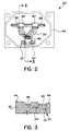
- the electronic package in accordance with the present invention is generally identified with the reference numeral 20.
- the electronic package 20 is formed with a composite housing 22, for example, an aluminum silicon carbide (AlSiC), configured for a particular electronic circuit application which does not form a part of the present invention.
- a composite housing 22 for example, an aluminum silicon carbide (AlSiC), configured for a particular electronic circuit application which does not form a part of the present invention.
- AlSiC aluminum silicon carbide
- FIGs. 1-3 An exemplary configuration for the housing 22 is illustrated in FIGs. 1-3.
- other composite materials can be used for housing 22.
- the ceramic preforms 24 may be cast with temperature durable electronic components, such as resistors, capacitors and inductors to form component preforms.
- the ceramic preforms 24 may also be configured to form interconnect channels 26 as well as feedthroughs 30.
- the ceramic preforms 24, in turn, are cast into the composite housing 22. Since the various electronic components, such as the coupling capacitors 32 and voltage dropping resistors 34 can be cast in the ceramic preform 24 and in turn cast into the composite housing 22, signal decoupling and signal conditioning circuitry can be disposed within the electronic package 20, relatively closely to the electronic circuit, for example an R.F. amplifier.
- the housing 22 may be formed with various component cavities, such as the cavities 36 and 38, for example, for receiving various non-temperature durable electronic components after the casting of the housing 22, such as integrated circuits (IC) and microwave monolithic integrated circuits (MMIC), identified with the reference numerals 40 and 42 respectively.
- IC integrated circuits
- MMIC microwave monolithic integrated circuits
- the IC's and/or MMIC's 40 and 42 are adapted to be disposed in the cavities 36 and 38 and securely attached thereto by way of a suitable adhesive after casting of the housing 22.
- the IC's and/or MMIC's 40 and 42 may be interconnected to the existing interconnection channel 26 and feed through 30 using electrical conductors 46, 48 and 50.
- the electrical conductors 46, 48, and 50 may be gold wire, gold ribbon, or gold mesh (other metals can also be used).
- Flip Chip An alternative process, commonly referred to as “Flip Chip,” can be used, which would allow the IC and/or MMIC 40 and 42 to be gold soldered to the interconnection channel 26 and feed through 30.
- a seal ring 44 may be cast into the housing 22.
- the seal ring 44 is best illustrated in FIG. 2.
- the seal ring 44 is adapted to seal the electronic components within the electronic package 20 against a cover plate (not shown).
- the cover plate may be attached to the seal ring by way of a conductive adhesive, such as a low temperature seal glass in order to seal the package 20 once the electronic components have been mounted inside.
- An important aspect of the invention relates to the method for making electrical interconnections between the various electronic components within the electronic package.
- ceramic preform interconnect channels 24 as well as ceramic preformed feedthroughs 30 may be cast into the housing 22 to form a structure, for example, as illustrated in FIG. 1.
- interconnect channels 24 and feedthrough preforms non-temperature durable electronic components, such as IC's as well as MMIC's 40 and 42, are disposed in the component cavities 36 and 38 and attached to the housing 22 by way of a suitable adhesive. Interconnections between the various components can be done in different ways. For example, as illustrated in FIG.
- electrical connections may be made between the components 32 and 40 and the interconnect channel 26 and feedthrough 30 using one or a variety of materials placed within the channel and/or feedthrough. These connections may be made by materials such as thick film metal paste, rigid metal wire or immersion plating. After these partial connections to 32 and 34 are made, the assembly may be placed into a mold pressure/vacuum chamber and exposed to a metal, for example, aluminum, under very high pressure and vacuum. Due to the porosity of the ceramic material used for the interconnect channels 26 and feedthrough 30, the metal will infuse into the ceramic, much like water into a sponge, filling any holes or gaps with the metal to form an electrical conductor in the interconnect channel 24 or feedthrough 30. In addition, intermetallic bonds are formed with any metal (i.e.
- any components electrically coupled to the interconnect channels 26 and feedthroughs 30 will be electrically bonded by way of the metal infusion.
- the need for glass feedthroughs is eliminated.
- the various ceramic preforms, numeral 24, are molded in a green state using a tool that is the mirror image of the desired shape.
- the ceramic preforms are also used for forming interconnect channels in order to interconnect various components within the electronic package as well as feedthroughs.
- the ceramic material forms a natural insulatative barrier. By selecting the diameter of the interconnect channels as well as the type of ceramic (i.e. dielectric value) one may create a particular desired impedance. Techniques for molding ceramic materials are well known within the art.
- the green ceramic is then fired to bake out organic material to produce a hard and microscopically porous preform.
- the various ceramic preforms 24 are then cast in the housing 22. As shown in FIG. 1, RF pins 52 and DC pads can be cast in during the metal infusion process. Solder pads 54 can also be cast rather simply and easily.
- the solder pads 54 are normally used for input/output (I/O) attachment.
- FIGs. 2 and 3 show an alternate configuration of the embodiment illustrated in FIG. 1.
- like components are identified with like reference numerals for simplification but with primes.
- This embodiment includes a pair of integrated circuits 40' and 42'.
- the electronic package 20' may include a regulator chip 60.
- the circuitry may also include a pair of decoupling capacitors 32' as well as a voltage dropping resistor 34'.
- ceramic preforms 24' may be used for interconnecting various components within the electronic package 20'.
- electrical connections between various components and the ceramic preforms 24' may be made by way of thick film metal paste, rigid metal wire, or immersion plating. Interconnections within the interconnect channels 26 are by metal infusion as discussed above.
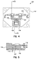
- FIGs. 4 and 5 An alternate embodiment of the electronic package is illustrated in FIGs. 4 and 5 and generally identified with the reference numeral 100.
- a base 102 which acts as a heat sink, is fabricated out of a suitable metal material, such as cooper.
- the base 102 is machined or cast to form the desired configuration, for example, as illustrated in FIG. 4.
- a polymer 104 (FIG. 5), such as liquid crystal polymer ("LCP"), is molded around the base 102.
- LCP liquid crystal polymer
- the base 102 may be formed along its edges with a step shape, for example, which allows the molded polymer 104 to interlock with the base 102 as shown.
- Various temperature durable components such as resistors 107, capacitors 106, inductors (not shown), and the like may be molded into the polymer 104.
- DC pins such as the DC pin 110 and RF pins, such as the RF pin 112 can also be molded into the polymer 104.
- interconnect metal traces 108 can be insert molded into the polymer 104 to form interconnect structures.
- the various electronic components can either be attached to the interconnect metal traces 108 prior to molding or molded into the polymer 104 without being connected.
- the polymer 104 may be molded with interconnection holes or cavities (not shown). These interconnection cavities may be filled with polymer based conductive paste or immersion plating in order to provide interconnection between the various components within the package.
- a microstrip substrate 109 can also be attached, for example, by way of an adhesive, to form input/output terminals.
- the package 100 may be plated.
- the plating process may be initially electro-less. All exposed metal surfaces (i.e. interconnect metal traces 108) are masked so that the plating does not short the metal traces 108. The entire part may then electroplated, if required, in order to complete the interconnections.
- integrated circuits and other non-temperature durable components may be attached directly to the base 102.
- a cover may be attached to the assembly using an adhesive, welding or fasteners to provide sealing protection for the components within the package.
Landscapes
- Lead Frames For Integrated Circuits (AREA)
- Fixed Capacitors And Capacitor Manufacturing Machines (AREA)
- Cooling Or The Like Of Semiconductors Or Solid State Devices (AREA)
Applications Claiming Priority (2)
| Application Number | Priority Date | Filing Date | Title |
|---|---|---|---|
| US08/932,474 US6261872B1 (en) | 1997-09-18 | 1997-09-18 | Method of producing an advanced RF electronic package |
| US932474 | 2004-09-01 |
Publications (2)
| Publication Number | Publication Date |
|---|---|
| EP0903785A2 true EP0903785A2 (fr) | 1999-03-24 |
| EP0903785A3 EP0903785A3 (fr) | 1999-08-11 |
Family
ID=25462384
Family Applications (1)
| Application Number | Title | Priority Date | Filing Date |
|---|---|---|---|
| EP98117198A Withdrawn EP0903785A3 (fr) | 1997-09-18 | 1998-09-09 | Empaquetage électronique RF avancé |
Country Status (4)
| Country | Link |
|---|---|
| US (2) | US6261872B1 (fr) |
| EP (1) | EP0903785A3 (fr) |
| JP (1) | JP3418125B2 (fr) |
| KR (1) | KR19990029740A (fr) |
Cited By (1)
| Publication number | Priority date | Publication date | Assignee | Title |
|---|---|---|---|---|
| WO2016205024A1 (fr) * | 2015-06-16 | 2016-12-22 | Ii-Vi Incorporated | Boîtier de dispositif électronique utilisant un composite de matrice métallique |
Families Citing this family (21)
| Publication number | Priority date | Publication date | Assignee | Title |
|---|---|---|---|---|
| US6507110B1 (en) * | 2000-03-08 | 2003-01-14 | Teledyne Technologies Incorporated | Microwave device and method for making same |
| US20020158305A1 (en) * | 2001-01-05 | 2002-10-31 | Sidharth Dalmia | Organic substrate having integrated passive components |
| DE10125815C1 (de) * | 2001-05-26 | 2002-08-01 | Daimler Chrysler Ag | Metall-Keramik-Verbundwerkstoff und seine Verwendung |
| KR100382765B1 (ko) * | 2001-06-15 | 2003-05-09 | 삼성전자주식회사 | 송수신용 수동소자와 그 집적모듈 및 그 제조방법 |
| US6788171B2 (en) * | 2002-03-05 | 2004-09-07 | Xytrans, Inc. | Millimeter wave (MMW) radio frequency transceiver module and method of forming same |
| US7535093B1 (en) * | 2002-03-08 | 2009-05-19 | Raytheon Company | Method and apparatus for packaging circuit devices |
| US6987307B2 (en) * | 2002-06-26 | 2006-01-17 | Georgia Tech Research Corporation | Stand-alone organic-based passive devices |
| US6900708B2 (en) * | 2002-06-26 | 2005-05-31 | Georgia Tech Research Corporation | Integrated passive devices fabricated utilizing multi-layer, organic laminates |
| US7260890B2 (en) | 2002-06-26 | 2007-08-28 | Georgia Tech Research Corporation | Methods for fabricating three-dimensional all organic interconnect structures |
| US20040080917A1 (en) * | 2002-10-23 | 2004-04-29 | Steddom Clark Morrison | Integrated microwave package and the process for making the same |
| US7489914B2 (en) * | 2003-03-28 | 2009-02-10 | Georgia Tech Research Corporation | Multi-band RF transceiver with passive reuse in organic substrates |
| US7115988B1 (en) * | 2004-01-21 | 2006-10-03 | Altera Corporation | Bypass capacitor embedded flip chip package lid and stiffener |
| US8345433B2 (en) * | 2004-07-08 | 2013-01-01 | Avx Corporation | Heterogeneous organic laminate stack ups for high frequency applications |
| US7439840B2 (en) | 2006-06-27 | 2008-10-21 | Jacket Micro Devices, Inc. | Methods and apparatuses for high-performing multi-layer inductors |
| US7808434B2 (en) * | 2006-08-09 | 2010-10-05 | Avx Corporation | Systems and methods for integrated antennae structures in multilayer organic-based printed circuit devices |
| US7989895B2 (en) | 2006-11-15 | 2011-08-02 | Avx Corporation | Integration using package stacking with multi-layer organic substrates |
| US7656236B2 (en) | 2007-05-15 | 2010-02-02 | Teledyne Wireless, Llc | Noise canceling technique for frequency synthesizer |
| US8179045B2 (en) | 2008-04-22 | 2012-05-15 | Teledyne Wireless, Llc | Slow wave structure having offset projections comprised of a metal-dielectric composite stack |
| US9202660B2 (en) | 2013-03-13 | 2015-12-01 | Teledyne Wireless, Llc | Asymmetrical slow wave structures to eliminate backward wave oscillations in wideband traveling wave tubes |
| US9454177B2 (en) | 2014-02-14 | 2016-09-27 | Apple Inc. | Electronic devices with housing-based interconnects and coupling structures |
| US9793227B1 (en) * | 2016-04-21 | 2017-10-17 | Peregrine Semiconductor San Diego | Switchable die seal connection |
Family Cites Families (48)
| Publication number | Priority date | Publication date | Assignee | Title |
|---|---|---|---|---|
| US2903627A (en) | 1957-03-29 | 1959-09-08 | Speer Carbon Company | Mounting for electric circuit components and printed circuit unit |
| US3401309A (en) | 1965-09-01 | 1968-09-10 | Shatz Solomon | Arrangement of electrical circuits and multiple electrical components |
| EP0001890B1 (fr) | 1977-10-12 | 1981-07-22 | The Secretary of State for Defence in Her Britannic Majesty's Government of the United Kingdom of Great Britain and | Perfectionnements aux boîtiers pour circuits intégrés à micro-ondes |
| JPS54136970U (fr) * | 1978-03-16 | 1979-09-22 | ||
| US4487999A (en) | 1983-01-10 | 1984-12-11 | Isotronics, Inc. | Microwave chip carrier |
| US4649417A (en) * | 1983-09-22 | 1987-03-10 | International Business Machines Corporation | Multiple voltage integrated circuit packaging substrate |
| US4547836A (en) | 1984-02-01 | 1985-10-15 | General Electric Company | Insulating glass body with electrical feedthroughs and method of preparation |
| US4647476A (en) | 1984-03-05 | 1987-03-03 | General Electric Company | Insulating glass body with electrical feedthroughs and method of preparation |
| JPS60210853A (ja) | 1984-03-06 | 1985-10-23 | Fujitsu Ltd | 半導体装置 |
| JPH0812887B2 (ja) | 1985-04-13 | 1996-02-07 | 富士通株式会社 | 高速集積回路パツケ−ジ |
| US4732780A (en) | 1985-09-26 | 1988-03-22 | General Electric Company | Method of making hermetic feedthrough in ceramic substrate |
| US4890663A (en) | 1987-05-21 | 1990-01-02 | Interatom Gmbh | Method for producing a ceramic-coated metallic component |
| US4841101A (en) | 1987-12-21 | 1989-06-20 | Pollock John A | Hermetically sealed feedthroughs and methods of making same |
| JPH01317155A (ja) * | 1988-03-04 | 1989-12-21 | Mitsubishi Kasei Corp | セラミック成形体の製造法 |
| FR2629271B1 (fr) * | 1988-03-25 | 1991-03-29 | Thomson Hybrides Microondes | Dispositif d'interconnexion et de protection d'une pastille nue de composant hyperfrequence |
| US4915719A (en) | 1988-09-30 | 1990-04-10 | Honeywell Inc. | Method of producing a hermetic glass to metal seal without metal oxidation |
| US5163499A (en) | 1988-11-10 | 1992-11-17 | Lanxide Technology Company, Lp | Method of forming electronic packages |
| US5526867A (en) | 1988-11-10 | 1996-06-18 | Lanxide Technology Company, Lp | Methods of forming electronic packages |
| US4899118A (en) | 1988-12-27 | 1990-02-06 | Hughes Aircraft Company | Low temperature cofired ceramic packages for microwave and millimeter wave gallium arsenide integrated circuits |
| US5136271A (en) * | 1989-01-09 | 1992-08-04 | Mitsubishi Denki Kabushiki Kaisha | Microwave integrated circuit mountings |
| US5175067A (en) | 1989-07-12 | 1992-12-29 | Medtronic, Inc. | Feed through |
| JP2528521B2 (ja) * | 1989-08-31 | 1996-08-28 | 日機装株式会社 | 表面積測定装置の測定レンジ自動切り替え装置 |
| EP0444820A3 (en) | 1990-02-26 | 1992-07-08 | Raytheon Company | Mmic package and connection |
| US5214498A (en) | 1990-02-26 | 1993-05-25 | Raytheon Company | MMIC package and connector |
| US5394930A (en) * | 1990-09-17 | 1995-03-07 | Kennerknecht; Steven | Casting method for metal matrix composite castings |
| US5138436A (en) | 1990-11-16 | 1992-08-11 | Ball Corporation | Interconnect package having means for waveguide transmission of rf signals |
| JPH04192353A (ja) * | 1990-11-26 | 1992-07-10 | Hitachi Ltd | 集積回路 |
| US5055966A (en) | 1990-12-17 | 1991-10-08 | Hughes Aircraft Company | Via capacitors within multi-layer, 3 dimensional structures/substrates |
| US5259436A (en) | 1991-04-08 | 1993-11-09 | Aluminum Company Of America | Fabrication of metal matrix composites by vacuum die casting |
| US5311920A (en) | 1991-07-29 | 1994-05-17 | Cook Arnold J | Method of forming a metal matrix component with internal and external structures |
| US5148135A (en) | 1991-09-04 | 1992-09-15 | Raytheon Company | Electronic hardware package |
| US5170142A (en) | 1991-09-09 | 1992-12-08 | Watkins-Johnson Company | Radio frequency feedthrough seal and method |
| US5185654A (en) | 1991-11-27 | 1993-02-09 | Motorola, Inc. | Electrostatic RF absorbant circuit carrier assembly and method for making the same |
| EP0547807A3 (en) * | 1991-12-16 | 1993-09-22 | General Electric Company | Packaged electronic system |
| US5384434A (en) | 1992-03-02 | 1995-01-24 | Murata Manufacturing Co., Ltd. | Multilayer ceramic circuit board |
| DE69318879T2 (de) * | 1992-04-03 | 1998-10-08 | Matsushita Electric Ind Co Ltd | Keramisches Mehrschicht-Substrat für hohe Frequenzen |
| US5376909A (en) | 1992-05-29 | 1994-12-27 | Texas Instruments Incorporated | Device packaging |
| US5422615A (en) | 1992-09-14 | 1995-06-06 | Hitachi, Ltd. | High frequency circuit device |
| US5365108A (en) | 1992-11-19 | 1994-11-15 | Sundstrand Corporation | Metal matrix composite semiconductor power switch assembly |
| US5347258A (en) | 1993-04-07 | 1994-09-13 | Zycon Corporation | Annular resistor coupled with printed circuit board through-hole |
| US5465008A (en) | 1993-10-08 | 1995-11-07 | Stratedge Corporation | Ceramic microelectronics package |
| US5455118A (en) | 1994-02-01 | 1995-10-03 | Pcc Composites, Inc. | Plating for metal matrix composites |
| US5532513A (en) * | 1994-07-08 | 1996-07-02 | Johnson Matthey Electronics, Inc. | Metal-ceramic composite lid |
| JPH08125110A (ja) * | 1994-10-25 | 1996-05-17 | Mitsubishi Heavy Ind Ltd | 機能可変型半導体モジュール |
| US5635761A (en) * | 1994-12-14 | 1997-06-03 | International Business Machines, Inc. | Internal resistor termination in multi-chip module environments |
| US5565262A (en) | 1995-01-27 | 1996-10-15 | David Sarnoff Research Center, Inc. | Electrical feedthroughs for ceramic circuit board support substrates |
| US5602421A (en) | 1995-01-31 | 1997-02-11 | Hughes Aircraft Company | Microwave monolithic integrated circuit package with improved RF ports |
| US5528076A (en) | 1995-02-01 | 1996-06-18 | Motorola, Inc. | Leadframe having metal impregnated silicon carbide mounting area |
-
1997
- 1997-09-18 US US08/932,474 patent/US6261872B1/en not_active Expired - Lifetime
-
1998
- 1998-04-08 US US09/057,041 patent/US6225696B1/en not_active Expired - Lifetime
- 1998-09-09 EP EP98117198A patent/EP0903785A3/fr not_active Withdrawn
- 1998-09-11 KR KR1019980037606A patent/KR19990029740A/ko not_active Ceased
- 1998-09-17 JP JP26292198A patent/JP3418125B2/ja not_active Expired - Fee Related
Cited By (1)
| Publication number | Priority date | Publication date | Assignee | Title |
|---|---|---|---|---|
| WO2016205024A1 (fr) * | 2015-06-16 | 2016-12-22 | Ii-Vi Incorporated | Boîtier de dispositif électronique utilisant un composite de matrice métallique |
Also Published As
| Publication number | Publication date |
|---|---|
| US6261872B1 (en) | 2001-07-17 |
| KR19990029740A (ko) | 1999-04-26 |
| JPH11154716A (ja) | 1999-06-08 |
| JP3418125B2 (ja) | 2003-06-16 |
| EP0903785A3 (fr) | 1999-08-11 |
| US6225696B1 (en) | 2001-05-01 |
Similar Documents
| Publication | Publication Date | Title |
|---|---|---|
| US6225696B1 (en) | Advanced RF electronics package | |
| US5359496A (en) | Hermetic high density interconnected electronic system | |
| US4925024A (en) | Hermetic high frequency surface mount microelectronic package | |
| US5006673A (en) | Fabrication of pad array carriers from a universal interconnect structure | |
| US5232548A (en) | Discrete fabrication of multi-layer thin film, wiring structures | |
| EP1186033B1 (fr) | Support de composants electroniques et procede de production de ce support | |
| US6262477B1 (en) | Ball grid array electronic package | |
| US7358604B2 (en) | Multichip circuit module and method for the production thereof | |
| US5604673A (en) | Low temperature co-fired ceramic substrates for power converters | |
| US5426405A (en) | Family of different-sized demountable hybrid assemblies with microwave-bandwidth interconnects | |
| JP3382677B2 (ja) | ハイブリッド回路 | |
| JPH0828441B2 (ja) | マイクロ波およびミリメータ波砒化ガリウム集積回路用の低温度共焼成セラミックパッケージ | |
| US20040080917A1 (en) | Integrated microwave package and the process for making the same | |
| US5227583A (en) | Ceramic package and method for making same | |
| US6108205A (en) | Means and method for mounting electronics | |
| EP0603158A2 (fr) | Perfectionement d'un boîtier à multicouches de plastique moulé utilisant la technologie "MESIC" | |
| CA2024784C (fr) | Substrat multicouche empilable pour le montage des circuits integres | |
| US5041695A (en) | Co-fired ceramic package for a power circuit | |
| US4901041A (en) | High-performance package for monolithic microwave integrated circuits | |
| EP0272046A2 (fr) | Structure de circuit comprenant un substrat composite en céramique | |
| US5512710A (en) | Multilayer package with second layer via test connections | |
| EP0235504A1 (fr) | Méthode d assembler une empaquetage à haute fréquence scellé hermétiquement pour composants à état solide | |
| US20070108584A1 (en) | Transmitter module with improved heat dissipation | |
| US20170290215A1 (en) | Electronic Assemblies without Solder and Methods for their manufacture | |
| EP0235503B1 (fr) | Empaquetage microélectronique hermétique à haute fréquence pour montage en surface |
Legal Events
| Date | Code | Title | Description |
|---|---|---|---|
| PUAI | Public reference made under article 153(3) epc to a published international application that has entered the european phase |
Free format text: ORIGINAL CODE: 0009012 |
|
| AK | Designated contracting states |
Kind code of ref document: A2 Designated state(s): DE FR GB IT |
|
| AX | Request for extension of the european patent |
Free format text: AL;LT;LV;MK;RO;SI |
|
| PUAL | Search report despatched |
Free format text: ORIGINAL CODE: 0009013 |
|
| AK | Designated contracting states |
Kind code of ref document: A3 Designated state(s): AT BE CH CY DE DK ES FI FR GB GR IE IT LI LU MC NL PT SE |
|
| AX | Request for extension of the european patent |
Free format text: AL;LT;LV;MK;RO;SI |
|
| RIC1 | Information provided on ipc code assigned before grant |
Free format text: 6H 01L 23/66 A, 6H 01L 23/498 B |
|
| 17P | Request for examination filed |
Effective date: 19990907 |
|
| AKX | Designation fees paid |
Free format text: DE FR GB IT |
|
| STAA | Information on the status of an ep patent application or granted ep patent |
Free format text: STATUS: THE APPLICATION IS DEEMED TO BE WITHDRAWN |
|
| 18D | Application deemed to be withdrawn |
Effective date: 20010403 |