EP0903750A1 - Method and circuit for generating programming and erasing voltage in nonvolatile memory - Google Patents
Method and circuit for generating programming and erasing voltage in nonvolatile memory Download PDFInfo
- Publication number
- EP0903750A1 EP0903750A1 EP98460036A EP98460036A EP0903750A1 EP 0903750 A1 EP0903750 A1 EP 0903750A1 EP 98460036 A EP98460036 A EP 98460036A EP 98460036 A EP98460036 A EP 98460036A EP 0903750 A1 EP0903750 A1 EP 0903750A1
- Authority
- EP
- European Patent Office
- Prior art keywords
- voltage
- circuit
- memory cells
- programming
- slope
- Prior art date
- Legal status (The legal status is an assumption and is not a legal conclusion. Google has not performed a legal analysis and makes no representation as to the accuracy of the status listed.)
- Granted
Links
Images

Classifications
-
- G—PHYSICS
- G11—INFORMATION STORAGE
- G11C—STATIC STORES
- G11C16/00—Erasable programmable read-only memories
- G11C16/02—Erasable programmable read-only memories electrically programmable
- G11C16/06—Auxiliary circuits, e.g. for writing into memory
- G11C16/10—Programming or data input circuits
- G11C16/12—Programming voltage switching circuits
-
- H—ELECTRICITY
- H03—ELECTRONIC CIRCUITRY
- H03K—PULSE TECHNIQUE
- H03K4/00—Generating pulses having essentially a finite slope or stepped portions
- H03K4/94—Generating pulses having essentially a finite slope or stepped portions having trapezoidal shape
Abstract
Description
La présente invention concerne un procédé et un circuit de génération de la tension de programmation ou d'effacement d'une cellule mémoire non volatile. L'invention trouve son application dans le domaine des mémoires non volatiles, programmables et effaçables électriquement (EPROM, EEPROM, flash).The present invention relates to a method and a programming voltage generation circuit or erase a non-volatile memory cell. The invention finds its application in the field of non-volatile, programmable and erasable memories electrically (EPROM, EEPROM, flash).
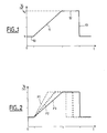
Les cellules mémoire de ces mémoires font appel à une technologie utilisant des transistors à grille flottante. Pour la programmation ou l'effacement d'une telle cellule mémoire, il est nécessaire de produire des hautes tensions de l'ordre de 15 à 20 volts. Ces tensions sont fournies soit par une source de tension externe, soit de manière interne par une pompe de charge intégrée dans la mémoire. La tension de programmation ou d'effacement appliquée sur une cellule mémoire est représentée à la figure 1. Elle comporte de manière classique
- une polarisation de départ à la tension
d'alimentation Vcc de la mémoire constituant un
premier plateau 10 en tension; - une rampe de tension constituée d'une phase
ascendante 11 pendant laquelle la tension grimpe de
façon linéaire jusqu'à une haute tension VH et
d'un plateau 12 en tension; et - une chute de
tension 13 pendant laquelle la tension revient à la valeur de la tension de départ.
- a starting bias at the supply voltage Vcc of the memory constituting a
first plateau 10 in voltage; - a voltage ramp consisting of an
ascending phase 11 during which the voltage increases linearly to a high voltage V H and of aplate 12 in tension; and - a voltage drop 13 during which the voltage returns to the value of the starting voltage.
La phase ascendante de la rampe de tension est
caractérisée par sa pente, laquelle est soumise à deux
conditions. Premièrement, elle ne doit pas être trop
élevée de manière à ne pas stresser l'oxyde de grille
de la cellule adressée. En effet, il est indispensable
que, pendant la phase ascendante, la variation du champ
électrique à l'intérieur de la cellule adressée ne soit
pas trop brutale pour ne pas fragiliser voire
détériorer l'oxyde de grille de la cellule.
Deuxièmement, le temps de montée de la rampe de tension
doit être calculé de manière à ce que la charge
capacitive adressée dans la mémoire n'agisse pas sur la
pente de la rampe. Il faut pour cela que la sortance S
de la pompe de charge chargée de fournir la haute
tension au circuit de génération de la rampe de tension
soit supérieure à la charge capacitive adressée C
multipliée par la pente de la rampe; c'est-à-dire il
faut que:
Pour que la relation (1) soit toujours vérifiée, il existe deux méthodes possibles:
- soit on prévoit une pompe de charge ayant une sortance élevée;
- soit on choisit une rampe de tension dont la pente est suffisamment faible pour que la relation (1) soit toujours vérifiée quelle que soit la charge capacitive adressée.
- either a charge pump having a high fan out is provided;
- or a voltage ramp is chosen whose slope is sufficiently low so that the relation (1) is always verified whatever the addressed capacitive load.
Ces deux méthodes présentent cependant quelques inconvénients. En ce qui concerne la première méthode, il n'est pas toujours possible d'augmenter la sortance de la pompe de charge. En effet, la pompe de charge est classiquement une pompe de Schenkel dont la sortance est proportionnelle à Ce*f/n et où Ce désigne la capacité d'un étage de la pompe, f désigne la fréquence de pompage et n désigne le nombre d'étages de la pompe. Augmenter la sortance de la pompe oblige à diminuer le nombre d'étages n, ce qui n'est pas possible car n fixe la tension délivrée par la pompe, ou à augmenter Ce ou f, ce qui est très coûteux en terme de place sur silicium. Sinon, la seconde méthode pénalise le temps d'écriture des cellules de la mémoire et donc la rapidité de la mémoire. Elle pénalise en particulier le fonctionnement de la mémoire en mode normal par rapport à celui en mode page ou en mode global.These two methods however have some drawbacks. With regard to the first method, it is not always possible to increase the fan out of the charge pump. Indeed, the charge pump is conventionally a Schenkel pump whose fanout is proportional to C e * f / n and where C e denotes the capacity of a stage of the pump, f denotes the pumping frequency and n denotes the number of pump stages. Increasing the fan out of the pump means reducing the number of stages n, which is not possible because n fixes the voltage delivered by the pump, or increasing C e or f, which is very costly in terms of space on silicon. Otherwise, the second method penalizes the writing time of memory cells and therefore the speed of memory. It penalizes in particular the functioning of the memory in normal mode compared to that in page mode or in global mode.
Un but de l'invention est de proposer un procédé de génération de la tension d'écriture dans une mémoire non volatile optimisant le temps d'écriture des cellules de la mémoire et un circuit mettant en oeuvre ce procédé. Selon l'invention, ce but est atteint et les inconvénients de l'art antérieur sont atténués ou supprimés en adaptant de manière dynamique la pente de la rampe à la charge capacitive adressée. Ainsi, les performances de la mémoire en matière de vitesse de programmation ou d'effacement s'adaptent aux besoins du client sans pour autant pénaliser la mémoire sur le plan de la surface sur silicium occupé par le circuit.An object of the invention is to propose a method for generating the write voltage in a memory non-volatile optimizing the writing time of memory cells and a circuit implementing this process. According to the invention, this object is achieved and the disadvantages of the prior art are mitigated or removed by dynamically adapting the slope of the ramp to the capacitive load addressed. So the memory performance in terms of speed of programming or erasing adapt to the needs of the client without penalizing memory on the plane of the surface on silicon occupied by the circuit.
L'invention a donc pour objet un procédé de programmation ou d'effacement des cellules mémoire d'une mémoire non volatile comprenant les étapes suivantes :
- produire une tension de programmation ou d'effacement comportant un front montant de tension sous forme de rampe de pente P, et
- appliquer cette tension de programmation ou d'effacement sur les cellules mémoire à programmer ou à effacer,
- producing a programming or erasing voltage comprising a rising voltage front in the form of a ramp of slope P, and
- apply this programming or erasing voltage to the memory cells to be programmed or erased,
Ainsi, des valeurs de pente différentes sont associées aux trois modes de fonctionnement de la mémoire (mode normal, mode page et mode global).So, different slope values are associated with the three operating modes of the memory (normal mode, page mode and global mode).
Dans un mode de réalisation préféré, la valeur de la pente en mode page est comprise entre une valeur minimale et une valeur maximale. Elle est définie entre ces deux valeurs limite en fonction du nombre de cellules mémoire adressées en mode page, ce nombre étant déterminé pendant une étape d'acquisition précédant la génération de la tension de programmation ou d'effacement.In a preferred embodiment, the value of the slope in page mode is between a value minimum and a maximum value. It is defined between these two limit values according to the number of memory cells addressed in page mode, this number being determined during an acquisition step preceding the generation of the programming voltage or erasure.
L'invention concerne également un circuit de programmation ou d'effacement des cellules mémoire d'une mémoire non volatile comportant
- un circuit de génération de tension d'écriture pour générer une tension de programmation ou d'effacement comprenant un front montant de tension sous forme de rampe de pente P, et
- des moyens de sélection pour appliquer ladite tension de programmation ou d'effacement sur les cellules mémoire à programmer ou à effacer,
- a write voltage generation circuit for generating a programming or erasing voltage comprising a rising voltage front in the form of a slope ramp P, and
- selection means for applying said programming or erasing voltage to the memory cells to be programmed or erased,
D'autres caractéristiques et avantages de l'invention apparaítront à la lecture de la description détaillée qui suit et qui est faite en référence aux dessins annexés dans lesquels :
- la figure 1, déjà décrite, est un diagramme temporel de la tension de programmation (ou d'effacement) appliquée sur une ou plusieurs cellules mémoire;
- la figure 2 est un diagramme temporel des tensions de programmation (ou d'effacement) pour une mémoire fonctionnant selon trois modes;
- la figure 3 est un schéma fonctionnel d'un circuit de programmation ou d'effacement d'une mémoire non volatile selon l'invention; et
- la figure 4 est un mode de réalisation du circuit de génération de la tension d'écriture selon l'invention.
- FIG. 1, already described, is a time diagram of the programming (or erasing) voltage applied to one or more memory cells;
- FIG. 2 is a time diagram of the programming (or erasing) voltages for a memory operating in three modes;
- Figure 3 is a block diagram of a programming or erasing circuit of a non-volatile memory according to the invention; and
- FIG. 4 is an embodiment of the circuit for generating the write voltage according to the invention.
Selon l'invention, on prévoit de moduler lors d'une opération d'écriture la pente de la rampe de la tension d'écriture en fonction du nombre de cellules mémoire adressées simultanément.According to the invention, provision is made to modulate during of a write operation the slope of the ramp of the write voltage as a function of the number of cells memory addressed simultaneously.
Une valeur de pente est donc définie pour chaque mode d'écriture de la mémoire. Elle est inversement proportionnelle au nombre de cellules mémoire destinées à recevoir simultanément la tension d'écriture. La tension Vs pour les trois modes de fonctionnement de la mémoire est représentée à la figure 2. La partie ascendante de cette tension présente une pente de valeur P1 en mode normal, une pente de valeur P2 en mode page et une pente de valeur P3 en mode global avec P1 > P2 > P3.A slope value is therefore defined for each memory write mode. Conversely, proportional to the number of memory cells intended to receive the write voltage simultaneously. The voltage Vs for the three operating modes of the memory is shown in Figure 2. The part ascending this voltage has a slope of value P1 in normal mode, a slope of value P2 in page mode and a slope of value P3 in global mode with P1> P2> P3.
La valeur P1 est calculée de manière à ce que, pour une sortance S donnée du circuit, la relation S > P1 * C1 soit vérifiée, C1 représentant la charge capacitive de huit cellules mémoire en parallèle. La valeur P1 est également majorée par une valeur limite, valeur à partir de laquelle le champ électrique est trop intense à l'intérieur de la cellule mémoire.The P1 value is calculated so that, for a given fanout S of the circuit, the relation S> P1 * C1 is checked, C1 representing the load capacitive of eight memory cells in parallel. The P1 value is also increased by a limit value, value from which the electric field is too intense inside the memory cell.
De manière identique, la valeur P2 vérifie la relation S > P2 * C2 où C2 représente la charge capacitive d'une page. Généralement, la taille d'une page est égale à 8, 16, 32 ou 64 octets. Dans un premier mode de réalisation, la valeur P2 est indépendante de la taille de la page et est donc prise égale à la valeur correspondant à une page de taille maximale, c'est-à-dire 64 octets. Dans un mode de réalisation amélioré décrit plus loin, on détermine la taille de la page dans une première étape et on génère une pente P2 qui est fonction de cette taille.Identically, the value P2 checks the relation S> P2 * C2 where C2 represents the charge capacitive of a page. Generally, the size of a page is equal to 8, 16, 32 or 64 bytes. In one first embodiment, the value P2 is independent of page size and is therefore taken equal to the value corresponding to a size page maximum, i.e. 64 bytes. In a mode of improved implementation described below, the page size in a first step and we generate a slope P2 which is a function of this size.
Enfin, la valeur P3 est déterminée de la même façon en fonction de la charge capacitive C3 en mode global.Finally, the value P3 is determined by the same way depending on the capacitive load C3 in mode global.
Selon l'invention, la variation de pente est obtenue en chargeant plus ou moins rapidement un condensateur. Un circuit mettant en oeuvre le procédé de l'invention est décrit aux figures 3 et 4. Il a pour but de produire une tension d'écriture Vs dont la pente de la rampe est fonction du mode de fonctionnement de la mémoire.According to the invention, the variation in slope is obtained by loading more or less quickly a capacitor. A circuit implementing the method of the invention is described in Figures 3 and 4. It has intended to produce a writing voltage Vs whose ramp slope is a function of the memory operation.
En référence à la figure 3, le circuit de
l'invention est constitué d'un circuit de génération de
tension d'écriture 31 qui délivre la tension d'écriture
Vs, laquelle est appliquée sur la ou les cellules
mémoire par l'intermédiaire de moyens de sélection 32
qui permettent de sélectionner les cellules mémoire à
programmer ou à effacer. Le circuit 31 est alimenté
avec une haute tension VH fournie par une pompe de
charge 33.With reference to FIG. 3, the circuit of the invention consists of a write
Le circuit 31 est détaillé à la figure 4. Il comprend principalement:
- un condensateur C dont le temps de charge correspond au temps de montée de la tension Vs,
- un circuit de régulation du courant de charge du condensateur C,
- un circuit de charge fixant le courant de charge du condensateur C,
- un circuit de commande du circuit de charge pour adapter la valeur du courant de charge au nombre de cellules mémoire à programmer ou à effacer simultanément, et
- un circuit de décharge du condensateur C.
- a capacitor C, the charging time of which corresponds to the rise time of the voltage Vs,
- a circuit for regulating the charge current of the capacitor C,
- a charging circuit fixing the charging current of the capacitor C,
- a charge circuit control circuit for adapting the value of the charge current to the number of memory cells to be programmed or erased simultaneously, and
- a capacitor C discharge circuit.
Pour obtenir une rampe de tension à la sortie du circuit, on vient charger le condensateur C avec un courant Icharge. La valeur de ce courant détermine le temps de charge du condensateur C et par là-même le temps de montée de la rampe de tension. Le courant de charge Icharge est fixé par un circuit de charge connecté à la borne inférieure du condensateur C.To obtain a voltage ramp at the output of the circuit, we just charge capacitor C with a current Icharge. The value of this current determines the charging time of capacitor C and thereby the rise time of the voltage ramp. The current of charge Icharge is fixed by a charge circuit connected to the lower terminal of capacitor C.
Le courant de charge Icharge dépend du mode d'écriture employé. Les trois modes d'écriture possibles sont : le mode page, le mode global et le mode normal (mode byte). Le circuit de charge est composé de trois branches montées en parallèle entre la borne inférieure du condensateur C et la masse. Chaque branche est constituée de deux transistors MOS à canal N montés en série. En mode normal, les transistors des trois branches sont passants afin de fixer un courant de charge important tandis que pour les deux autres modes, seules deux des trois branches sont passantes.The charging current Icharge depends on the mode employee writing. The three writing modes possible are: page mode, global mode and normal mode (byte mode). The charging circuit is composed of three branches mounted in parallel between the lower terminal of capacitor C and ground. Each branch consists of two channel MOS transistors N mounted in series. In normal mode, the transistors of three branches are passing in order to fix a current significant load while for the other two modes, only two of the three branches are busy.
La première branche est constituée de deux transistors T1 et T2. Le transistor T1 est commandé par un signal issu d'une porte logique A1 de type ET qui reçoit sur ses entrées des signaux CHARGE et MODEGLOBAL-. Le signal CHARGE est actif pendant la charge du condensateur C et le signal MODEGLOBAL- l'est quand la mémoire n'est pas en mode global. Le transistor T2 reçoit sur sa grille une tension de référence constante UREF et est utilisé comme source de courant constant.The first branch consists of two transistors T1 and T2. The transistor T1 is controlled by a signal from a logic gate A1 of the AND type which receives on its inputs signals CHARGE and MODEGLOBAL-. The CHARGE signal is active during the charging of capacitor C and the MODEGLOBAL- signal is active when the memory is not in global mode. The transistor T2 receives a constant reference voltage U REF on its gate and is used as a constant current source.
La deuxième branche comporte deux transistors T3 et T4. Le transistor T3 est commandé par le signal CHARGE et le transistor T4 est commandé par la tension UREF. Enfin, la troisième branche comprend deux transistors T5 et T6. Le transistor T5 est commandé par le signal issu d'une porte logique A2 de type ET qui reçoit sur ses entrées le signal CHARGE et un signal MODEPAGE-. Le signal MODEPAGE- est un signal logique actif quand la mémoire n'est pas en mode page. Le transistor T6 reçoit sur sa grille la tension UREF et est équivalent à une source de courant constant. La valeur du courant Icharge est déterminée par la taille des transistors T2, T4 et T6. Par ailleurs, les transistors T1, T2 et T3 fonctionnent en saturation et sont utilisés comme interrupteurs.The second branch has two transistors T3 and T4. The transistor T3 is controlled by the signal CHARGE and the transistor T4 is controlled by the voltage U REF . Finally, the third branch includes two transistors T5 and T6. The transistor T5 is controlled by the signal from an AND type logic gate A2 which receives on its inputs the CHARGE signal and a MODEPAGE- signal. The MODEPAGE- signal is an active logic signal when the memory is not in page mode. The transistor T6 receives the voltage U REF on its gate and is equivalent to a constant current source. The value of the current Icharge is determined by the size of the transistors T2, T4 and T6. Furthermore, the transistors T1, T2 and T3 operate in saturation and are used as switches.
En mode normal, le courant de charge Icharge est égal à la somme des courants imposés par les transistors T2, T4 et T6. En mode page, le condensateur est chargé uniquement par le courant imposé par les transistors T2 et T4. Enfin, en mode global, le courant de charge est égal à la somme des courants imposés par les transistors T4 et T6.In normal mode, the charging current Icharge is equal to the sum of the currents imposed by the transistors T2, T4 and T6. In page mode, the capacitor is charged only by the current imposed by the transistors T2 and T4. Finally, in global mode, the current load is equal to the sum of the currents imposed by transistors T4 and T6.
La taille des transistors T2, T4 et T6 fixe la valeur des courants de charge des trois modes. Pour une page de X octets, la charge capacitive est X fois plus élevée qu'en mode normal; il en résulte que la taille du transistor T2 est (X-1) fois plus élevé que celle du transistor T4 si on désire que la valeur du courant de charge soit inversement proportionnelle à la charge capacitive adressée. Dans la pratique, cela n'est pas réalisé car le circuit serait beaucoup trop couteux en terme de silicium. C'est pourquoi, dans l'exemple de la figure 4, on choisit trois valeurs de courant de charge I1, I2, I3 respectivement pour le mode normal, le mode page et le mode global définies de la manière suivante: I1 = 10*I2 = 20*I3, et dont les pentes respectives P1, P2 et P3 vérifient la relation (1). Les rapports W/L des transistors du circuit de charge sont donc les suivants : W/L(T4)=1; W/L(T2)=19 et W/L(T6)=9. Dans cet exemple, on choisit de pénaliser le temps d'écriture en mode normal pour limiter la taille des transistors T2 et T6, cependant ce temps d'écriture reste bien plus faible que dans une mémoire classique. Il s'agit là de réaliser un compromis entre la taille du circuit (taille des transistors du circuit de charge) et le gain en vitesse d'écriture.The size of the transistors T2, T4 and T6 fixes the charge current values of the three modes. For a page of X bytes, the capacitive load is X times more high than in normal mode; it follows that the size of transistor T2 is (X-1) times higher than that of transistor T4 if we want the current value of load is inversely proportional to the load capacitive addressed. In practice, this is not realized because the circuit would be much too expensive in silicon term. This is why, in the example of the figure 4, we choose three load current values I1, I2, I3 respectively for normal mode, mode page and global mode defined as follows: I1 = 10 * I2 = 20 * I3, and whose respective slopes P1, P2 and P3 verify the relation (1). W / L ratios load circuit transistors are therefore the following: W / L (T4) = 1; W / L (T2) = 19 and W / L (T6) = 9. In this example, we choose to penalize the writing time by normal mode to limit the size of T2 transistors and T6, however this writing time remains much longer weak than in conventional memory. This is about compromise between the size of the circuit (size of the load circuit transistors) and the gain in writing speed.
Le circuit 31 comporte par ailleurs un circuit de
régulation du courant de charge alimenté par la tension
VH correspondant à la valeur maximale de la tension Vs.
Il comporte un transistor MOS à canal N, T7, dont le
drain reçoit la tension VH et dont la source est
connectée à la borne supérieure du condensateur C. Sa
grille est par ailleurs connectée au drain d'un
transistor MOS à canal P, T8. La tension VH est
appliquée sur la source de ce dernier et une tension de
polarisation VP légèrement inférieure à la tension VH
est appliquée sur sa grille.The
Le circuit de régulation du courant de charge comporte également un transistor T9 dont la grille est reliée à la borne inférieure du condensateur C, dont le drain est connecté au drain du transistor T8 et dont la source est reliée à la masse par l'intermédiaire d'un transistor T10 monté en diode. Le transistor T10 est utilisé ici comme résistance. La régulation du courant se fait de la manière suivante: si le courant de charge diminue, le potentiel sur la borne inférieure du condensateur C diminue et le transistor T9 devient plus résistant. Le potentiel sur la grille du transistor T7 augmente alors, le transistor T7 devient moins résistant et le courant de charge augmente.The load current regulation circuit also includes a transistor T9 whose gate is connected to the lower terminal of capacitor C, the drain is connected to the drain of transistor T8 and whose source is connected to ground via a transistor T10 mounted as a diode. The transistor T10 is used here as resistance. Current regulation is done as follows: if the charging current decreases, the potential on the lower bound of the capacitor C decreases and transistor T9 becomes more resistant. The potential on the gate of transistor T7 then increases, transistor T7 becomes less resistant and the charging current increases.
Le circuit 31 comporte également un circuit de
décharge connecté entre la borne supérieure du
condensateur C et la masse. Ce circuit de décharge
comprend deux transistors T11 et T12 montés en série.
Le transistor est commandé par un signal DECHARGE actif
pendant la phase de décharge du condensateur C. Le
transistor T12 est commandé par la tension UREF et est
dimensionné de manière à décharger très rapidement le
condensateur C. La taille du transistor T12 fixe la
valeur de ce courant de décharge.The
Enfin, le circuit comporte un dispositif pour
générer la tension de référence de la tension
d'écriture représenté à la figure 1. Dans l'exemple de
la figure 4, la tension de référence est égale à la
tension d'alimentation Vcc de la mémoire. Ce dispositif
comporte deux transistors MOS à canal N, T13 et T14,
dont le drain est alimenté par la tension VH et dont la
grille est connectée au drain du transistor T8 du
circuit de régulation. La source du transistor T13 est
connectée à la tension d'alimentation Vcc par
l'intermédiaire d'un transistor MOS à canal P, T15. La
grille du transistor T15 est reliée à la source du
transistor T14. Ainsi lorsque la tension de grille des
transistors T13 et T14 est faible, le transistor T15
est passant et impose la tension Vcc sur la source du
transistor T13. Un transistor supplémentaire T16 à
canal N est prévu pour annuler la tension Vs lorsque le
circuit est désactivé (signal RAZ à l'état haut). La
tension d'écriture Vs est prélevée sur la source du
transistor T13. Enfin, le circuit est complété par un
transistor T17 à canal N pour faire chuter la tension
Vs (chute en tension 13 sur la figure 1) en fin
d'opération. Ce transistor est commandé par un signal S
actif pendant la phase 13 de la tension Vs.Finally, the circuit includes a device for generating the reference voltage of the write voltage represented in FIG. 1. In the example of FIG. 4, the reference voltage is equal to the supply voltage Vcc of the memory . This device comprises two N-channel MOS transistors, T13 and T14, the drain of which is supplied by the voltage V H and the gate of which is connected to the drain of the transistor T8 of the regulation circuit. The source of transistor T13 is connected to the supply voltage Vcc via a P-channel MOS transistor, T15. The gate of transistor T15 is connected to the source of transistor T14. Thus when the gate voltage of the transistors T13 and T14 is low, the transistor T15 is on and imposes the voltage Vcc on the source of the transistor T13. An additional N-channel transistor T16 is provided to cancel the voltage Vs when the circuit is deactivated (reset signal at high state). The write voltage Vs is taken from the source of the transistor T13. Finally, the circuit is completed by an N-channel transistor T17 to cause the voltage Vs to drop (
Le circuit fonctionne de la manière suivante :
pendant une phase de charge correspondant à la phase
ascendante de la tension Vs, le condensateur C se
charge et la tension à ses bornes augmente
progressivement. La valeur du courant Icharge est plus
ou moins élevée suivant l'état des signaux MODEPAGE- et
MODEGLOBAL-. Dans la suite de la description, les
potentiels PT1 et PT2 désignent respectivement le
potentiel sur la grille du transistor T13 et le
potentiel sur la borne inférieure du condensateur. A
mesure que le potentiel de la borne supérieure du
condensateur C augmente, le potentiel PT1 et la tension
Vs augmentent. Il arrive un moment où le potentiel PT1
atteint un maximum. Le condensateur C continuant à se
charger, le potentiel PT2 s'abaisse. Quand le potentiel
PT2 devient alors inférieur à la valeur seuil du
transistor T9, celui-ci se bloque. La charge est alors
interrompue et la décharge du condensateur est amorcée.
Pendant la phase de décharge, la tension Vs est
maintenue à sa valeur maximale car le transistor T9 est
bloqué. Pendant cette phase, la tension Vs présente un
plateau en tension (référencé 12 sur la figure 1). Le
potentiel sur la borne supérieure du condensateur chute
au fur et à mesure que le condensateur se décharge et
le signal DECHARGE est désactivé lorsque ce potentiel
passe en dessous d'un potentiel seuil. A ce moment
précis, le signal S devient actif, le transistor T17
devient passant et la tension Vs chute (phase 13 sur la
figure 1) jusqu'à la valeur de référence Vcc imposé par
le transistor T15.The circuit works as follows:
during a charging phase corresponding to the phase
rising from voltage Vs, capacitor C
load and the voltage across it increases
gradually. Icharge current value is more
or lower depending on the state of the MODEPAGE- and
MODEGLOBAL-. In the following description, the
potentials PT1 and PT2 respectively designate the
potential on the gate of transistor T13 and the
potential on the lower terminal of the capacitor. AT
measure that the potential of the upper bound of the
capacitor C increases, the potential PT1 and the voltage
They increase. There comes a time when the potential PT1
reaches a maximum. The capacitor C continuing to
charge, the PT2 potential drops. When the potential
PT2 then becomes lower than the threshold value of the
transistor T9, this one blocks. The charge is then
interrupted and the discharge of the capacitor is initiated.
During the discharge phase, the voltage Vs is
maintained at its maximum value because transistor T9 is
blocked. During this phase, the voltage Vs presents a
tension plate (referenced 12 in Figure 1). The
potential on the upper terminal of the capacitor drops
as the capacitor discharges and
the DISCHARGE signal is deactivated when this potential
goes below a potential threshold. At the moment
precise, signal S becomes active, transistor T17
becomes conducting and the voltage Vs falls (
Ce circuit a été conçu pour produire une tension d'écriture Vs particulière pour chaque mode d'écriture de la mémoire.This circuit was designed to produce a voltage Vs write mode for each write mode from memory.
Dans un mode de réalisation amélioré, on peut envisager d'affiner la pente de la tension Vs en mode page en tenant compte du nombre exact de cellules mémoire adressées par page. Pour se faire, il suffit de faire un comptage des cellules mémoire adressées en mode page avant de générer la tension Vs et d'associer à la valeur obtenue une valeur de courant de charge particulière. En pratique, on compte le nombre d'impulsions Nh d'horloge nécessaires pour charger la page dans les circuits tampons de la mémoire avant la programmation de la page dans les cellules de la mémoire et on adapte le courant de charge en mode page à ce nombre. Il suffit par exemple d'un compteur 6 bits (comptage jusqu'à 64) pour acquérir le nombre Nh et de quatre transistors identiques montés en parallèle à la place du transistor T2 imposant chacun un courant de charge I. A la suite de l'étape de comptage ou phase d'acquisition, on active:
- quatre transistors si Nh < 8,
- trois transistors si 8 ≤ Nh < 16,
- deux transistors si 16 ≤ Nh < 32, et
- un transistor si Nh ≥ 32.
- four transistors if Nh <8,
- three transistors if 8 ≤ Nh <16,
- two transistors if 16 ≤ Nh <32, and
- a transistor if Nh ≥ 32.
Le courant de charge est alors fonction du nombre d'octets compris dans une page.The charging current is then a function of the number bytes included in a page.
Claims (7)
en ce qu'il impose une première valeur de courant de charge lorsque les transistors des trois groupes sont passants, une seconde valeur de courant de charge lorsque les transistors des premier et second groupes sont passants, et une troisième valeur de courant de charge lorsque les transistors des second et troisième groupes sont passants.Circuit according to Claim 6, characterized in that the charging circuit comprises a plurality of transistors connected in parallel and distributed in three groups, and
in that it imposes a first load current value when the transistors of the three groups are on, a second load current value when the transistors of the first and second groups are on, and a third load current value when the transistors of the second and third groups are on.
Applications Claiming Priority (2)
| Application Number | Priority Date | Filing Date | Title |
|---|---|---|---|
| FR9711912 | 1997-09-19 | ||
| FR9711912A FR2768846B1 (en) | 1997-09-19 | 1997-09-19 | METHOD AND CIRCUIT FOR GENERATING PROGRAMMING AND ERASE VOLTAGE IN A NON-VOLATILE MEMORY |
Publications (2)
| Publication Number | Publication Date |
|---|---|
| EP0903750A1 true EP0903750A1 (en) | 1999-03-24 |
| EP0903750B1 EP0903750B1 (en) | 2000-11-15 |
Family
ID=9511448
Family Applications (1)
| Application Number | Title | Priority Date | Filing Date |
|---|---|---|---|
| EP98460036A Expired - Lifetime EP0903750B1 (en) | 1997-09-19 | 1998-09-10 | Method and circuit for generating programming and erasing voltage in nonvolatile memory |
Country Status (4)
| Country | Link |
|---|---|
| US (1) | US5995416A (en) |
| EP (1) | EP0903750B1 (en) |
| DE (1) | DE69800399T2 (en) |
| FR (1) | FR2768846B1 (en) |
Cited By (3)
| Publication number | Priority date | Publication date | Assignee | Title |
|---|---|---|---|---|
| EP1058271A1 (en) * | 1999-06-04 | 2000-12-06 | STMicroelectronics S.r.l. | CMOS switch circuit for transferring high voltages, in particular for line decoding in nonvolatile memories, with reduced consumption during switching |
| FR2809246A1 (en) * | 2000-05-17 | 2001-11-23 | St Microelectronics Sa | Slope generator for low voltage drop in series, for use in electrically programmable and erasable memory units |
| FR2821974A1 (en) * | 2001-03-12 | 2002-09-13 | St Microelectronics Sa | CIRCUIT AND ASSOCIATED METHOD FOR ERASING OR PROGRAMMING A MEMORY CELL |
Families Citing this family (8)
| Publication number | Priority date | Publication date | Assignee | Title |
|---|---|---|---|---|
| IT1303204B1 (en) * | 1998-11-27 | 2000-10-30 | St Microelectronics Srl | HIGH-PRECISION NON-VOLATILE MEMORY CELLS PROGRAMMING METHOD, WITH OPTIMIZED PROGRAMMING SPEED. |
| TW505365U (en) * | 2002-02-08 | 2002-10-01 | Hon Hai Prec Ind Co Ltd | Computer housing |
| KR100748553B1 (en) * | 2004-12-20 | 2007-08-10 | 삼성전자주식회사 | Apparatus and method for generating ripple-free high voltage and semiconductor memory device having the same |
| KR100830575B1 (en) * | 2006-09-26 | 2008-05-21 | 삼성전자주식회사 | Flash memory device and multi-block erase method thereof |
| KR101390337B1 (en) * | 2007-09-13 | 2014-04-29 | 삼성전자주식회사 | Multi-level phase change memory device, program method thereof, and memory system including the same |
| US9082510B2 (en) * | 2012-09-14 | 2015-07-14 | Freescale Semiconductor, Inc. | Non-volatile memory (NVM) with adaptive write operations |
| FR3041807B1 (en) * | 2015-09-24 | 2017-12-08 | Stmicroelectronics Rousset | METHOD FOR CONTROLLING AN EEPROM TYPE MEMORY WRITE CYCLE AND CORRESPONDING DEVICE |
| JP6741811B1 (en) * | 2019-03-07 | 2020-08-19 | 力晶積成電子製造股▲ふん▼有限公司Powerchip Semiconductor Manufacturing Corporation | Erase control circuit and method for nonvolatile semiconductor memory device, and nonvolatile semiconductor memory device |
Citations (2)
| Publication number | Priority date | Publication date | Assignee | Title |
|---|---|---|---|---|
| JPS57176826A (en) * | 1981-04-22 | 1982-10-30 | Hitachi Ltd | Ramp function voltage generator |
| EP0762428A1 (en) * | 1995-09-05 | 1997-03-12 | STMicroelectronics S.A. | Method and circuit for programming and erasing a memory |
Family Cites Families (2)
| Publication number | Priority date | Publication date | Assignee | Title |
|---|---|---|---|---|
| JP3976839B2 (en) * | 1996-07-09 | 2007-09-19 | 株式会社ルネサステクノロジ | Nonvolatile memory system and nonvolatile semiconductor memory |
| KR100232190B1 (en) * | 1996-10-01 | 1999-12-01 | 김영환 | Nonvolatile semiconductor memory device |
-
1997
- 1997-09-19 FR FR9711912A patent/FR2768846B1/en not_active Expired - Fee Related
-
1998
- 1998-09-10 DE DE69800399T patent/DE69800399T2/en not_active Expired - Lifetime
- 1998-09-10 EP EP98460036A patent/EP0903750B1/en not_active Expired - Lifetime
- 1998-09-18 US US09/156,945 patent/US5995416A/en not_active Expired - Lifetime
Patent Citations (2)
| Publication number | Priority date | Publication date | Assignee | Title |
|---|---|---|---|---|
| JPS57176826A (en) * | 1981-04-22 | 1982-10-30 | Hitachi Ltd | Ramp function voltage generator |
| EP0762428A1 (en) * | 1995-09-05 | 1997-03-12 | STMicroelectronics S.A. | Method and circuit for programming and erasing a memory |
Non-Patent Citations (3)
| Title |
|---|
| LUBIN GEE ET AL: "An enhaced 16K E2PROM", IEEE JOURNAL OF SOLID-STATE CIRCUITS., vol. 17, no. 5, October 1982 (1982-10-01), NEW YORK US, pages 828 - 832, XP002066751 * |
| LUCERO ET AL: "A 16 kbit smart 5V-only EEPROM with redundancy", IEEE JOURNAL OF SOLID-STATE CIRCUITS., vol. 18, no. 5, October 1983 (1983-10-01), NEW YORK US, pages 539 - 544, XP002066699 * |
| PATENT ABSTRACTS OF JAPAN vol. 7, no. 17 (E - 154)<1162> 22 January 1983 (1983-01-22) * |
Cited By (6)
| Publication number | Priority date | Publication date | Assignee | Title |
|---|---|---|---|---|
| EP1058271A1 (en) * | 1999-06-04 | 2000-12-06 | STMicroelectronics S.r.l. | CMOS switch circuit for transferring high voltages, in particular for line decoding in nonvolatile memories, with reduced consumption during switching |
| US6433583B1 (en) | 1999-06-04 | 2002-08-13 | Stmicroelectronics S.R.L. | CMOS switch circuit for transferring high voltages, in particular for line decoding in nonvolatile memories, with reduced consumption during switching |
| FR2809246A1 (en) * | 2000-05-17 | 2001-11-23 | St Microelectronics Sa | Slope generator for low voltage drop in series, for use in electrically programmable and erasable memory units |
| FR2821974A1 (en) * | 2001-03-12 | 2002-09-13 | St Microelectronics Sa | CIRCUIT AND ASSOCIATED METHOD FOR ERASING OR PROGRAMMING A MEMORY CELL |
| EP1246197A1 (en) * | 2001-03-12 | 2002-10-02 | STMicroelectronics S.A. | Circuit and method for erasing or programming a memory cell |
| US6621737B2 (en) | 2001-03-12 | 2003-09-16 | Stmicroelectronics Sa | Circuit and associated method for the erasure or programming of a memory cell |
Also Published As
| Publication number | Publication date |
|---|---|
| DE69800399D1 (en) | 2000-12-21 |
| DE69800399T2 (en) | 2001-03-15 |
| EP0903750B1 (en) | 2000-11-15 |
| FR2768846B1 (en) | 1999-12-24 |
| US5995416A (en) | 1999-11-30 |
| FR2768846A1 (en) | 1999-03-26 |
Similar Documents
| Publication | Publication Date | Title |
|---|---|---|
| EP0318363B1 (en) | Method for testing cells of electrically programmable memories and a corresponding integrated circuit | |
| EP0903750B1 (en) | Method and circuit for generating programming and erasing voltage in nonvolatile memory | |
| EP0743650B1 (en) | Current detector circuit for reading integrated circuit memory | |
| EP0762428B1 (en) | Method and circuit for programming and erasing a memory | |
| FR2817413A1 (en) | Device for switching higher supply voltage for use in read-only memory store, comprising circuit for subjecting drop in gate voltage of switching transistor to voltage of output line | |
| FR2665973A1 (en) | Automatic erase optimisation circuit for an electrically erasable and programmable semiconductor memory, and method relating thereto | |
| EP0562916A1 (en) | Device for generating reference voltages | |
| FR2798218A1 (en) | HIGH DENSITY NOR-TYPE FLASH MEMORY DEVICE AND ITS PROGRAMMING PROCESS | |
| EP0788233B1 (en) | Power on reset circuit | |
| FR2843660A1 (en) | Two switching levels programmable circuit having first/second units with different threshold level zero signal set with erasable electrical programmes and output delivered either circuit | |
| EP3147909B1 (en) | Method for controlling an eeprom memory write cycle and corresponding device | |
| EP0902437A1 (en) | High-voltage generating circuit for programming or erasing a memory | |
| FR2838861A1 (en) | Electrically erasable and programmable memory comprising a device for managing an internal voltage supply | |
| FR2770326A1 (en) | EEPROM memory cell and data writing circuit | |
| FR2750240A1 (en) | Feedback loop reference voltage generator | |
| EP3605403B1 (en) | Programmable artificial neuron and associated programming method | |
| EP1246197B1 (en) | Circuit and method for erasing or programming a memory cell | |
| EP0872848B1 (en) | Memory read circuit with dynamically controlled precharge arrangement | |
| EP0811987B1 (en) | Circuit to produce high programming voltage | |
| FR2858457A1 (en) | Non-volatile memory e.g. flash memory, cell erasing or programming method, involves applying memory cell state fixation pulse on floating gate of transistor, and adjusting cell state fixing portion at preset duration | |
| FR2847717A1 (en) | Voltage-limiting circuit for use at the output of an over-voltage circuit such as charge pump used for obtaining voltage higher than the supply voltage, in particular for memory circuits | |
| FR3094829A1 (en) | Process for writing electrically erasable and programmable non-volatile memory and corresponding integrated circuit | |
| FR2769747A1 (en) | Hot carrier programmable memory used in nonvolatile and programmable integrated circuit memories | |
| EP1109026B1 (en) | Apparatus for detecting a high voltage | |
| EP0420822B1 (en) | Method of storing analogue values and device for its implementation |
Legal Events
| Date | Code | Title | Description |
|---|---|---|---|
| PUAI | Public reference made under article 153(3) epc to a published international application that has entered the european phase |
Free format text: ORIGINAL CODE: 0009012 |
|
| AK | Designated contracting states |
Kind code of ref document: A1 Designated state(s): DE FR GB IT |
|
| AX | Request for extension of the european patent |
Free format text: AL;LT;LV;MK;RO;SI |
|
| 17P | Request for examination filed |
Effective date: 19990712 |
|
| AKX | Designation fees paid |
Free format text: DE FR GB IT |
|
| GRAG | Despatch of communication of intention to grant |
Free format text: ORIGINAL CODE: EPIDOS AGRA |
|
| 17Q | First examination report despatched |
Effective date: 20000228 |
|
| GRAG | Despatch of communication of intention to grant |
Free format text: ORIGINAL CODE: EPIDOS AGRA |
|
| GRAH | Despatch of communication of intention to grant a patent |
Free format text: ORIGINAL CODE: EPIDOS IGRA |
|
| GRAH | Despatch of communication of intention to grant a patent |
Free format text: ORIGINAL CODE: EPIDOS IGRA |
|
| GRAA | (expected) grant |
Free format text: ORIGINAL CODE: 0009210 |
|
| AK | Designated contracting states |
Kind code of ref document: B1 Designated state(s): DE FR GB IT |
|
| GBT | Gb: translation of ep patent filed (gb section 77(6)(a)/1977) |
Effective date: 20001115 |
|
| REF | Corresponds to: |
Ref document number: 69800399 Country of ref document: DE Date of ref document: 20001221 |
|
| ITF | It: translation for a ep patent filed |
Owner name: BOTTI & FERRARI S.R.L. |
|
| PLBE | No opposition filed within time limit |
Free format text: ORIGINAL CODE: 0009261 |
|
| STAA | Information on the status of an ep patent application or granted ep patent |
Free format text: STATUS: NO OPPOSITION FILED WITHIN TIME LIMIT |
|
| 26N | No opposition filed | ||
| REG | Reference to a national code |
Ref country code: GB Ref legal event code: IF02 |
|
| PGFP | Annual fee paid to national office [announced via postgrant information from national office to epo] |
Ref country code: IT Payment date: 20070913 Year of fee payment: 10 |
|
| PGFP | Annual fee paid to national office [announced via postgrant information from national office to epo] |
Ref country code: GB Payment date: 20080827 Year of fee payment: 11 |
|
| PGFP | Annual fee paid to national office [announced via postgrant information from national office to epo] |
Ref country code: FR Payment date: 20080929 Year of fee payment: 11 |
|
| PG25 | Lapsed in a contracting state [announced via postgrant information from national office to epo] |
Ref country code: IT Free format text: LAPSE BECAUSE OF NON-PAYMENT OF DUE FEES Effective date: 20080910 |
|
| GBPC | Gb: european patent ceased through non-payment of renewal fee |
Effective date: 20090910 |
|
| REG | Reference to a national code |
Ref country code: FR Ref legal event code: ST Effective date: 20100531 |
|
| PG25 | Lapsed in a contracting state [announced via postgrant information from national office to epo] |
Ref country code: FR Free format text: LAPSE BECAUSE OF NON-PAYMENT OF DUE FEES Effective date: 20090930 |
|
| PG25 | Lapsed in a contracting state [announced via postgrant information from national office to epo] |
Ref country code: GB Free format text: LAPSE BECAUSE OF NON-PAYMENT OF DUE FEES Effective date: 20090910 |
|
| REG | Reference to a national code |
Ref country code: DE Ref legal event code: R082 Ref document number: 69800399 Country of ref document: DE Representative=s name: BEETZ & PARTNER PATENT- UND RECHTSANWAELTE, DE |
|
| REG | Reference to a national code |
Ref country code: DE Ref legal event code: R082 Ref document number: 69800399 Country of ref document: DE Representative=s name: BEETZ & PARTNER MBB PATENT- UND RECHTSANWAELTE, DE Effective date: 20140704 Ref country code: DE Ref legal event code: R082 Ref document number: 69800399 Country of ref document: DE Representative=s name: BEETZ & PARTNER MBB, DE Effective date: 20140704 Ref country code: DE Ref legal event code: R082 Ref document number: 69800399 Country of ref document: DE Representative=s name: BEETZ & PARTNER PATENT- UND RECHTSANWAELTE, DE Effective date: 20140704 Ref country code: DE Ref legal event code: R081 Ref document number: 69800399 Country of ref document: DE Owner name: MICRON TECHNOLOGY, INC., BOISE, US Free format text: FORMER OWNER: STMICROELECTRONICS S.A., GENTILLY, FR Effective date: 20140704 |
|
| PGFP | Annual fee paid to national office [announced via postgrant information from national office to epo] |
Ref country code: DE Payment date: 20170905 Year of fee payment: 20 |
|
| REG | Reference to a national code |
Ref country code: DE Ref legal event code: R071 Ref document number: 69800399 Country of ref document: DE |