JP3976839B2 - Nonvolatile memory system and nonvolatile semiconductor memory - Google Patents
Nonvolatile memory system and nonvolatile semiconductor memory Download PDFInfo
- Publication number
- JP3976839B2 JP3976839B2 JP12679397A JP12679397A JP3976839B2 JP 3976839 B2 JP3976839 B2 JP 3976839B2 JP 12679397 A JP12679397 A JP 12679397A JP 12679397 A JP12679397 A JP 12679397A JP 3976839 B2 JP3976839 B2 JP 3976839B2
- Authority
- JP
- Japan
- Prior art keywords
- state
- memory cell
- data
- write
- memory
- Prior art date
- Legal status (The legal status is an assumption and is not a legal conclusion. Google has not performed a legal analysis and makes no representation as to the accuracy of the status listed.)
- Expired - Fee Related
Links
Images


Classifications
-
- G—PHYSICS
- G11—INFORMATION STORAGE
- G11C—STATIC STORES
- G11C16/00—Erasable programmable read-only memories
- G11C16/02—Erasable programmable read-only memories electrically programmable
- G11C16/06—Auxiliary circuits, e.g. for writing into memory
-
- G—PHYSICS
- G11—INFORMATION STORAGE
- G11C—STATIC STORES
- G11C16/00—Erasable programmable read-only memories
- G11C16/02—Erasable programmable read-only memories electrically programmable
- G11C16/06—Auxiliary circuits, e.g. for writing into memory
- G11C16/34—Determination of programming status, e.g. threshold voltage, overprogramming or underprogramming, retention
- G11C16/3418—Disturbance prevention or evaluation; Refreshing of disturbed memory data
- G11C16/3427—Circuits or methods to prevent or reduce disturbance of the state of a memory cell when neighbouring cells are read or written
-
- G—PHYSICS
- G11—INFORMATION STORAGE
- G11C—STATIC STORES
- G11C16/00—Erasable programmable read-only memories
- G11C16/02—Erasable programmable read-only memories electrically programmable
- G11C16/04—Erasable programmable read-only memories electrically programmable using variable threshold transistors, e.g. FAMOS
- G11C16/0491—Virtual ground arrays
-
- G—PHYSICS
- G11—INFORMATION STORAGE
- G11C—STATIC STORES
- G11C16/00—Erasable programmable read-only memories
- G11C16/02—Erasable programmable read-only memories electrically programmable
- G11C16/06—Auxiliary circuits, e.g. for writing into memory
- G11C16/10—Programming or data input circuits
- G11C16/12—Programming voltage switching circuits
-
- G—PHYSICS
- G11—INFORMATION STORAGE
- G11C—STATIC STORES
- G11C16/00—Erasable programmable read-only memories
- G11C16/02—Erasable programmable read-only memories electrically programmable
- G11C16/06—Auxiliary circuits, e.g. for writing into memory
- G11C16/10—Programming or data input circuits
- G11C16/14—Circuits for erasing electrically, e.g. erase voltage switching circuits
- G11C16/16—Circuits for erasing electrically, e.g. erase voltage switching circuits for erasing blocks, e.g. arrays, words, groups
-
- G—PHYSICS
- G11—INFORMATION STORAGE
- G11C—STATIC STORES
- G11C16/00—Erasable programmable read-only memories
- G11C16/02—Erasable programmable read-only memories electrically programmable
- G11C16/06—Auxiliary circuits, e.g. for writing into memory
- G11C16/34—Determination of programming status, e.g. threshold voltage, overprogramming or underprogramming, retention
- G11C16/3404—Convergence or correction of memory cell threshold voltages; Repair or recovery of overerased or overprogrammed cells
-
- G—PHYSICS
- G11—INFORMATION STORAGE
- G11C—STATIC STORES
- G11C16/00—Erasable programmable read-only memories
- G11C16/02—Erasable programmable read-only memories electrically programmable
- G11C16/06—Auxiliary circuits, e.g. for writing into memory
- G11C16/34—Determination of programming status, e.g. threshold voltage, overprogramming or underprogramming, retention
- G11C16/3418—Disturbance prevention or evaluation; Refreshing of disturbed memory data
- G11C16/3431—Circuits or methods to detect disturbed nonvolatile memory cells, e.g. which still read as programmed but with threshold less than the program verify threshold or read as erased but with threshold greater than the erase verify threshold, and to reverse the disturbance via a refreshing programming or erasing step
-
- G—PHYSICS
- G11—INFORMATION STORAGE
- G11C—STATIC STORES
- G11C16/00—Erasable programmable read-only memories
- G11C16/02—Erasable programmable read-only memories electrically programmable
- G11C16/06—Auxiliary circuits, e.g. for writing into memory
- G11C16/34—Determination of programming status, e.g. threshold voltage, overprogramming or underprogramming, retention
- G11C16/3436—Arrangements for verifying correct programming or erasure
- G11C16/3454—Arrangements for verifying correct programming or for detecting overprogrammed cells
- G11C16/3459—Circuits or methods to verify correct programming of nonvolatile memory cells
-
- G—PHYSICS
- G11—INFORMATION STORAGE
- G11C—STATIC STORES
- G11C2216/00—Indexing scheme relating to G11C16/00 and subgroups, for features not directly covered by these groups
- G11C2216/12—Reading and writing aspects of erasable programmable read-only memories
- G11C2216/18—Flash erasure of all the cells in an array, sector or block simultaneously
Description
【0001】
【発明の属する技術分野】
この発明は、半導体記憶装置さらには不揮発性半導体記憶装置における情報書込み方式に適用して特に有効な技術に関し、例えば複数の記憶情報を電気的に一括消去可能な不揮発性メモリシステムおよび不揮発性半導体メモリに利用して有効な技術に関するものである。
【0002】
【従来の技術】
フラッシュメモリは、コントロールゲートおよびフローティングゲートを有する不揮発性記憶素子をメモリセルに使用しており、1個のトランジスタ(MOSFET)でしきい値電圧を情報として記憶するメモリセルを構成することができる。かかるフラッシュメモリにおいては、書き込み動作では、図18に示すように、不揮発性記憶素子のドレイン電圧を例えば5V(ボルト)にし、コントロールゲートCGが接続されたワード線を例えば−10Vにすることにより、フローティングゲートFGから電荷をドレイン領域へ引き抜いて、しきい値電圧を低い状態(論理“0”)にする。消去動作では、図19に示すように、ウェル領域を例えば−5Vにし、コントローゲートCGを10Vのような高電圧にしてフローティングゲートFGに負電荷を注入してしきい値を高い状態(論理“1”)にする。これにより、1つのメモリセルに1ビットのデータを記憶させるようにしている。
【0003】
【発明が解決しようとする課題】
従来のフラッシュメモリは、一本のワード線に複数のメモリセルのコントロールゲートが接続され、このワード線に接続される複数のメモリセルを単位(以下、この単位をセクタと称する)として、消去、書込み、読出しがそれぞれの動作モードに区別されて行なわれてきた。まず消去は、ワード線を共通にする複数のメモリセルに対して同時に行われる。この消去はセクタ単位で行われ、複数のメモリセルのうち特定のメモリセルだけを選択的に消去することはできない。
【0004】
一方、書込みは、一旦消去を行なって図20(a)のようにしきい値を高くしてから、しきい値を下げようとするメモリセルが接続されたワード線に−10Vを印加しドレインに5V、ソースに0Vを印加して行なうようにしていた。これによって、書込みを行なったメモリセルのしきい値は、図20(b)のようにベリファイ電圧Vpvよりも低くなる。このとき、書込みが行なわれないつまりしきい値を下げないメモリセルのドレインには0Vが印加されていたが、上記書込みセルとワード線を共通にする他のメモリセルのゲートには−10Vのような大きな電圧が印加されるため、しきい値が僅かに下がる現象が起きる。書込みを行う特定のメモリセルのしきい値電圧だけが変化することが望ましいが、書込みを行わないメモリセルにもわずかにではあるがしきい値の変化が起こる。この望ましくないしきい値電圧の変化は、ディスターブと呼ばれる。かかるディスターブ現象は、主にワード線に電圧が印加されることによって起こるため、ワード線ディスターブ(またはワードディスターブ)と呼ばれる。
【0005】
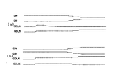
上記のワードディスターブにより、セクタ単位のメモリセルは一括消去を行わずに書込みを繰り返し行うことは困難であった。この様子を、図20(c)から(f)に示す。最初に同じワード線に接続される複数のメモリセルを一括消去すると、この複数のメモリセルのしきい値はすべて最も高い消去レベルとなる(図20(a))。次に書込みを行い、特定のメモリセルのしきい値を選択的に書込み状態にする(図20(b))。この時、複数のメモリセルは、しきい値電圧が消去状態の第1メモリセル群(図20(c)の点線)と、しきい値電圧が書込み状態の第2メモリセル群(図20(d)の点線)とからなる。選択的なメモリセルの消去はできないので、書込みを行えるのは第1メモリセルに限られる。そこで、第1メモリセル群のいずれかを選択して書込みを行う。この時、ワードディスターブが起こると、図20(c)及び(d)のように書込みを行わなかったメモリセルのしきい値電圧が低下する。
【0006】
一括消去を行わずに書込みを繰り返し行うことで、ディスターブが何度か繰り返されると、メモリセルのしきい値が図20(e)のようにデータ読出し時のワード線レベルVr よりも低くなって、誤まったデータの読出しが行なわれてしまう。また、図20(f)のように接地電位Vssより低くなって非選択時にもオン状態となってしまい、ワード線は異にするがソース線は共通であるメモリセルを選択したときに、データ線上の電荷が上記接地電位Vssよりもしきい値の低いメモリセルを通してソースに流れてしまうため、誤まったデータの読出しが行なわれるおそれがあるという問題点があった。
【0007】
なお、メモリアレイの構成によっては、しきい値の低い状態を消去状態とし、書込みによってメモリセルのしきい値を高くする方式もあるが、かかる書込み方式においても、書込み時にワード線を共通にする非書込みのメモリセルのしきい値が僅かに高くなるというディスターブ現象がある(図21(c),(d)参照)。そして、ディスターブが何度か繰り返されると、メモリセルのしきい値が図21(e)のようにデータ読出し時のワード線レベルVr よりも高くなって誤まったデータの読出しが行なわれるおそれがある。
【0008】
図22に、一本のワード線で管理されるセクタの情報マットを示す。例えば、図20(a−1)〜(a−3)では一本のワード線に512byte(4096bit)のメモリセルが接続される。ここで、図22に示すように、同一セクタ内にOS情報(オペレーションシステムに関する情報)やセクタ管理情報等一般ユーザーに開放されていない記憶領域(以下、システム領域と称する)と、一般ユーザーが自由に書込みをできる記憶領域(以下、ユーザー領域と称する)とを混在して設けることでメモリの有効利用を図ることができる。実際にはシステム領域はユーザ領域に比べるとほんの僅かである。このような記憶方式のフラッシュメモリは、システム領域に所定のデータが書き込まれ、ユーザー領域は未書込みの状態でユーザーに提供される。大きな情報エリアを持つユーザ領域の消去状態にあるメモリセルを選択して繰り返し書込みを行う追加書込みと呼ばれる動作が行えると便利である。しかるに、従来のフラッシュメモリを使用したシステムでは、ディスターブのため記憶情報の保証ができなくなるためそのような追加書込み動作が行なわれていなかった。また、追加書込みを許容したとしてもディスターブによるしきい値変動を考慮して連続して追加書込みを行う回数を大幅に制限する必要性があった。
【0009】
また、メモリ自身も上記のような使用の仕方を考慮して設計されていなかった。そのため、従来のフラッシュメモリで追加書込みを行なうとすると、通常の書込みと同一のアルゴリズムすなわち一旦当該セクタのデータを外部へ読み出してセクタの一括消去を行なってから、上記読出しデータと追加書込みデータとを合成して書込みを行なわなくてはならないため、追加書込みに要する時間が非常に長くなるとともに、ソフトウェアの負担が大きくなってしまうという不具合があることが明らかになった。
【0010】
この発明の目的は、ワード線ディスターブによるメモリセルのしきい値の変動を回復させることが可能な不揮発性メモリシステムおよび不揮発性半導体メモリを提供することにある。
【0011】
この発明の他の目的は、一括消去を行わずに追加書込みの連続実行が可能な不揮発性メモリシステムおよび不揮発性半導体メモリを提供することにある。
【0012】
この発明の他の目的は、追加書込みという動作を通常の書込みよりも高速で行なうことができ、しかも追加書込みにおけるソフトウェアの負担を軽減することが可能な不揮発性メモリシステムおよび不揮発性半導体メモリを提供することにある。
【0013】
この発明の前記ならびにほかの目的と新規な特徴は、本明細書の記述及び添付図面から明らかになるであろう。
【0014】
【課題を解決するための手段】
本願において開示される発明のうち代表的なものを概要を簡単に説明すれば、下記のとおりである。
【0015】
すなわち、所定の指令が与えられると、指定アドレスのセクタの記憶データを読み出してレジスタに退避させてから当該セクタの一括消去を行ない、前記退避されたデータと追加書込みしようとするデータとから実際の書込みデータ(以下、書込み期待値データと称する)を形成して書込み動作を行なうように構成したものである。
【0016】
また、しきい値電圧の第1状態(例えばしきい値電圧の高い消去状態)と第2状態(例えばしきい値電圧の低い書込み状態)とにより情報を記憶する複数のメモリセルと、前記複数のメモリセルのコントロールゲートに接続されるワード線とを有するメモリアレイと、コマンド入力端子を有し前記コマンド入力端子に入力される命令に従って前記複数のメモリセルの消去および書込みの動作を所定の手順に従って制御するシーケンサとを備え、前記シーケンサの受ける前記命令には、複数のメモリセルのしきい値電圧を一括して第1状態に変化させる消去コマンドと、前記複数のメモリセルのうちしきい値電圧が第1状態にあるメモリセルの少なくとも一つを選択的に第2状態に変化させる追加書込みコマンドとを含み、前記追加書込みコマンド、前記消去コマンドを実行せずに複数回連続してデータの書込みを実行可能であるように不揮発性メモリシステムを構成する。
【0017】
さらに、好適な実施形態においては、前記複数のメモリセルのうち、しきい値電圧が第1状態にあるメモリセルを第1メモリセル群とし、しきい値電圧が第2状態にあるメモリセルを第2メモリセル群とするときに、前記シーケンサは、前記追加書込みコマンドが入力されると、前記第2メモリセル群のしきい値電圧を前記第1状態と第2状態との間にする第1のステップを実行した後、前記第1メモリセル群の少なくとも一つを選択的に前記第2状態にするとともに、前記第2メモリセル群のメモリセルのしきい値電圧を前記第2状態とする第2のステップを実行するように構成される。
【0018】
さらに、別の好適な実施形態においては、前記シーケンサの受ける前記命令には、複数のメモリセルのしきい値電圧を一括して第1状態に変化させる消去コマンドと、前記複数のメモリセルに含まれる選択された第1メモリセル群のしきい値電圧を前記第2状態に変化させるために前記ワード線に第2電圧を印加する手順を含む第1書込みコマンドと、前記複数のメモリセルのしきい値電圧を前記第2状態から第1状態の電圧方向に変化させるために前記ワード線に第1電圧を印加した後に、前記複数のメモリセルに含まれる選択された第2メモリセル群のしきい値電圧を前記第2状態に変化させるために前記ワード線に第2電圧を印加する手順を含む第2書込みコマンドとが含まれるようにする。
【0019】
これによって、追加書込みの際にワード線ディスターブによるメモリセルのしきい値の変動が回復され、誤まったデータの読み出しを防止することができる。結果として、消去命令を実行せずに追加書込みを連続して実行できる回数を大幅に増加させることができる。
【0020】
また、選択セクタから読み出され内部レジスタに保持したデータと、外部から入力した追加書込みデータを用いて、書込み期待値データを自動的に内部で形成してから書込み動作を行なうように構成することにより、追加書込みという動作を通常の書込みよりも高速で行なうことができ、しかも追加書込みにおけるソフトウェアの負担を軽減することができる。
【0021】
【発明の実施の形態】
以下、本発明をフラッシュメモリに適用した場合の実施例を図面を用いて説明する。
<実施例1>
図1には、本発明を適用したフラッシュメモリの一実施例が示されている。特に制限されないが、図1に示されている各回路ブロックは、単結晶シリコンのような1個の半導体チップ1上に形成されている。
【0022】
図1において、11は図18に示されているようなフローティングゲートを有する1つのトランジスタからなるメモリセルがマトリックス状に配置されたメモリアレイ、12はメモリアレイ11から読み出された1セクタ分のデータを保持したり外部から入力された書込みデータを保持するデータレジスタ、13は上記メモリアレイ11とデータレジスタ12との間に設けられた追加書込みや書換えの際のデータ変換を行なう書換回路である。
【0023】
また、14は外部から入力されたアドレス信号を保持するアドレスレジスタ、15はメモリアレイ11内のワード線の中から上記アドレスレジスタ14に取り込まれたアドレスに対応した1本のワード線を選択するXデコーダ、16は外部からの書込みデータを上記データレジスタ12に順次転送したりデータレジスタ12に読み出されたデータを外部へ出力するためのYアドレス信号(データ線選択信号)を生成するYアドレスカウンタである。上記Yアドレスカウンタ16は、1セクタの先頭アドレスから最終アドレスまでを順次更新し出力する機能を有する。17は生成されたYアドレスをデコードして1セクタ内の1つのデータを選択するYデコーダ、18はデータレジスタ12に読み出されたデータを増幅して外部へ出力するメインアンプである。
【0024】
この実施例のフラッシュメモリは、特に制限されないが、シリアルアクセスのデータ入出力インタフェースを持つ。例えば読出し時には、読み出すべきセクタのアドレスが入力されると一本のワード線が選択され、それに接続される複数のメモリセルから並行してデータが読み出され、それぞれ後に説明するセンスラッチ群SLTに一旦保持される。このセンスラッチ群は上記データレジスタ12に含まれる。センスラッチ群はYアドレスカウンタ16により順次選択され、その保持データがシリアルに出力される。書込みの場合は、シリアルデータが入力され、上記とは逆の経路で選択されたセクタに書込みが行われる。また、メモリチップの入出力端子は複数とされ、1セクタのデータが分割してシリアルに入力される。
【0025】
この実施例のフラッシュメモリは、特に制限されないが、外部のCPU等から与えられるコマンドを保持しそれをデコードするコマンドレジスタ&デコーダ21と、該コマンドレジスタ&デコーダ21のデコード結果に基づいて当該コマンドに対応した処理を実行すべくメモリ内部の各回路に対する制御信号を順次形成して出力する制御回路(シーケンサ)22とを備えており、コマンドが与えられるとそれを解読して自動的に対応する処理を開始するように構成されている。
【0026】
上記制御回路22は、例えばマイクロプログラム方式のCPUの制御部と同様に、コマンド(命令)を実行するのに必要な一連のマイクロ命令郡が格納されたROM(リードオンリメモリ)からなり、コマンドレジスタ&デコーダ21がコマンドに対応したマイクロ命令群の先頭アドレスを生成して制御回路22に与えることにより、マイクロプログラムが起動されるように構成することができる。このROM内に設けられたソフトウェアには、図4で後述する命令手順と、電圧印加時間等の条件とが格納される。ROMには最低限のマイクロ命令のみを搭載し、命令条件や追加プログラムは書換可能なフラッシュメモリに格納するようにしてもよい。
【0027】
さらに、この実施例のフラッシュメモリには、上記各回路の他、アドレス信号やデータ信号の入出力を行なうI/Oバッファ回路23、外部のCPU等から供給される制御信号が入力される制御信号入力バッファ回路24、外部から供給される電源電圧Vccに基づいて書込み電圧Vw(−10V)、消去電圧Ve(10V)、読出し電圧(2V)、ベリファイ電圧(1V)等チップ内部で必要とされる電圧を生成する電源回路25、メモリの動作状態に応じてこれらの電圧の中から所望の電圧を選択してメモリアレイ11やXデコーダ15に供給する電源切替回路26等が設けられている。なお、電源電圧よりも高いVwやVeのような電圧は、電源回路25に含まれるチャージポンプ回路により発生される。
【0028】
特に制限されないが、この実施例のフラッシュメモリは、アドレス信号と書込みデータ信号およびコマンド入力とで外部端子(ピン)I/Oを共用している。そのため、上記I/Oバッファ回路23は、上記制御信号入力バッファ回路24からの制御信号に従ってこれらの入力信号を区別して取り込み所定の内部回路に供給するように構成されている。
【0029】
外部のCPU等からこの実施例のフラッシュメモリに入力される制御信号としては、例えばリセット信号RESやチップ選択信号CE、書込み制御信号WE、出力制御信号OE、コマンドもしくはデータ入力かアドレス入力かを示すためのコマンドイネーブル信号CDE、システムクロックSC等がある。
【0030】
なお、上記実施例のフラッシュメモリを制御する外部の装置としては、アドレス生成機能とコマンド生成機能を備えていればよいので、汎用マイクロコンピュータLSIを用いることができる。
【0031】
図2には書込みによってメモリセルのしきい値を下げる方式のメモリアレイ11の具体例を示す。この実施例のメモリアレイ11は2つのマットで構成されており、図2にはそのうち片方のメモリマットの具体例が示されている。同図に示すように、各メモリマットは、列方向に配列され各々ソースおよびドレインが共通接続された並列形態のn個のメモリセル(フローティングゲートを有するMOSFET)MC1〜MCnからなるメモリ列MCCが行方向(ワード線WL方向)および列方向(データ線DL方向)にそれぞれ複数個配設されている。各メモリ列MCCは、n個のメモリセルMC1〜MCnのドレインおよびソースがそれぞれ共通のローカルデータ線LDLおよび共通のローカルソース線LSLに接続され、ローカルデータ線LDLは選択MOSFET Qs1を介してメインデータ線DLに、またローカルソース線LSLは選択MOSFET Qs2を介して接地点または負電圧に接続可能にされた構成にされている。上記複数のメモリ列MCCのうちワード線方向に配設されているものは半導体基板上の同一のウェル領域WELL内に形成される。
【0032】
特に制限されないが、図2に示すメモリアレイの構成を有し、消去状態を高いしきい値電圧にとるとともに書込み状態を低いしきい値電圧にとる方式はAND形フラッシュメモリと呼ばれることがある。この場合、フローティングゲートへの電子の注入(しきい値電圧を上げ、消去状態にする)には、特に制限されないが、トランジスタのチャネルからFN(Fowler-Nordheim)トンネル注入が用いられ、フローティングゲートからの電子の引き抜き(しきい値電圧を下げ、書込み状態にする)には、拡散層へのFNトンネル放出が用いられる。
【0033】
データ消去時にはそのウェル領域WELLおよびローカルソース線LSLに−3Vのような負電圧を与え、ウェル領域を共通にするワード線に10Vのような電圧を印加することで、一括消去が可能にされている。なお、データ消去時には選択MOSFET Qs2がオン状態にされて、各メモリセルのソースに−3Vの負電圧が印加されるように構成されている。このとき、選択MOSFET Qs1はオフとされ、ドレインは、コントロールゲートに10Vの高電圧が印加されることでオン状態にされたメモリセルのチャンネルを通してソース側の電圧が伝えられることで−3Vのような電位にされる。
【0034】
一方、データ書込み時には、選択されるメモリセルが接続されたワード線に−10Vのような負電圧が印加されるとともに、選択されるメモリセルに対応したメインデータ線DLが3Vのような電位にされかつ選択メモリセルが接続されたローカルデータ線LDL上の選択MOSFET Qs1がオン状態され、ドレインに3Vが印加される。ただし、このときローカルソース線LSL上の選択MOSFET Qs2はオフ状態とされている。
【0035】
また、データ読出し時には、選択されるメモリセルが接続されたワード線に読出し電圧Vr(例えば2.0V)のような電圧が印加されるとともに、選択されるメモリセルに対応したメインデータ線DLが1Vのような電位にプリチャージされかつ選択メモリセルが接続されたローカルデータ線LDL上の選択MOSFET Qs1がオン状態とされる。そして、このときローカルソース線LSL上の選択MOSFET Qs2はオン状態とされ、接地電位(0V)が印加される。これにより、メモリセルのしきい値電圧に応じて電流が流れるもの(LDL電位が0Vに低下)と、電流が流れないもの(LDL電位が1Vに維持される)とが区別され、メモリセルの記憶情報が読み出される。
【0036】
ここで、データ書込み時および消去時の電圧が図18,図19の従来タイプに比べて低いのは、従来より微細加工が可能な技術を使用して素子寸法を小さくするとともに、電源電圧Vccとして従来の5Vに代えて3Vを使用しているためである。
【0037】
上記メインデータ線DLの一端(メモリアレイの中央側)には読出し時にデータ線のレベルを検出するとともに書込み時に書込みデータに応じた電位を与えるセンスラッチ回路SLTと追加書込みの際に期待値データを形成したりするのに使用するデータ反転回路WRWがそれぞれ接続されている。上記センスラッチ回路SLTの集合が図1におけるデータレジスタ12で、データ反転回路WRWの集合が図1における書換回路13である。この2つのウェル領域WELL上に形成された2つのメモリアレイをマットa(MATa)と呼ぶこととする。ここで、メインデータ線の数やセンスラッチ回路SLTは1セクタに対応した数とされ、例えば4224個(512+16byte)が並列に設けられる。
【0038】
この実施例ではメモリアレイは2つのメモリマットで構成され、センスラッチ回路SLTの反対側すなわち図の下側にも上記データ反転回路WRWとメモリマットが配置されており、そのメモリアレイ内の各メインデータ線DLが対応するデータ反転回路WRWを介してセンスラッチ回路SLTの他方の入出力端子に接続されている。即ち、データ反転回路WRWはマットMATa及びMATbごとに設けられ(区別するときはWRWa,WRWbと呼ぶ)、センスラッチ回路SLTは2つのメモリマットで共用される。
【0039】
図3には、上記センスラッチ回路SLTおよびデータ反転回路WRWの具体的回路例を示す。回路はセンスラッチ回路を挟んで対称であるため、一方のメモリマット内の1本のデータ線に関してのみ図示するとともに、便宜上、データ線に接続されているメモリ列のうち1つのメモリ列MCCのみ示したが、実際には複数のメモリ列MCCが接続されるものである。図示のごとく、センスラッチ回路SLTはPチャネルMOSFETとNチャネルMOSFETからなる2つのCMOSインバータの入出力端子が交差結合されたフリップフロップ回路FFにより構成されている。そして、上記センスラッチ回路SLTの一対の入出力端子Na,Nbに、Yデコーダの出力によってオン、オフ制御されるいわゆるYゲートを構成するカラムスイッチMOSFET Qya、Qybが接続されている。このメインデータ線ごとに設けられた複数のカラムスイッチQya,Qybの他端は、相補共通入出力線(IO,/IO)に共通接続される。
【0040】
データ反転回路WRWaは、上記センスラッチ回路SLTの一方の入出力端子Naと一方のメモリマット内のメインデータ線DLaとの間に接続された伝送MOSFET Qt1と、電源電圧端子Vccとメインデータ線DLaとの間に接続され制御信号PC2Aによって制御されるプリチャージ用のMOSFET Qp1と、プリチャージ切替端子VPCとメインデータ線DLaとの間に直列接続されたMOSFETQt2,Qp2とにより構成されている。このうちQt2のゲートには、上記センスラッチ回路SLTの入出力端子Naの電位が印加され、Qp2のゲートには制御信号PC1Aが印加されている。また、上記プリチャージ切替端子VPCには電源電圧VccまたはVssが供給されるように構成されている。
【0041】
さらに、上記センスラッチ回路SLTの他方の入出力端子Nbにも同様の構成のMOSFETQt1,Qt2,Qp1,Qp2からなるデータ反転回路WRWbが接続されている。
【0042】
図4に制御回路22によるデータ追加書込み時の制御手順を示す。追加書込みを起動する追加書込みコマンドは、図1の制御入力信号のうち、コマンドイネーブル信号CDEが有効とされるとき、IO入出力端子から入力されるコマンドにより設定された8ビットのコードにより指定される。後に説明するように、この制御回路は、この他に消去コマンドや書込みコマンド等を受け付けるが、それらはIO入出力端子から入力されるコードの違いにより区別される。コマンドコードはコマンドデコーダによりデコードされ、それにより対応する一連のプログラムが起動される。
【0043】
この制御シーケンスは、追加書込みコマンドがコマンドレジスタ&デコーダ21に取り込まれることによって開始される。この制御シーケンスが開始されると、チップ内部が追加書込みモードにセットアップされ、データレジスタ12ではすべてのセンスラッチSLTに“1”がセットされる(ステップS1)。次に、外部から入力された書込みアドレスをアドレスレジスタ14に取り込む(ステップS2)。続いて、外部から入力された少なくとも1つの追加書込みデータをデータレジスタ12に格納する(ステップS3)。
【0044】
次に、外部から書込み開始コマンドがコマンドレジスタ&デコーダ21に取り込まれることによって、上記アドレスレジスタ14に保持されているセクタアドレス(Xアドレス)がXデコーダ15でデコードされ、メモリアレイ11内の1本のワード線が選択されて2Vのような読み出しレベルに設定される。これによって、1セクタ分のデータがデータレジスタ12に読み出されるとともに、すでにセットされていた追加書込みデータとに基づいて書込み期待値データを作成してそれをデータレジスタ12に保持させる(ステップS4)。以上の処理が前記制御回路(シーケンサ)22の制御の下で書換回路13(データ反転回路WRW)によって自動的に行なわれる。
【0045】
続いて、上記選択ワード線に10V、ウェル領域に−3Vの消去パルスを印加して当該セクタのすべてのメモリセルのしきい値を高める(ステップS5)。このステップが本願の特徴とするところの一つである。これによって、記憶データが論理“0”であったメモリセルは図10(C-1)のようにしきい値がVev以上となり、記憶データは論理“1”に変化するとともに、記憶データが論理“1”であったメモリセルは図10(B-1)のようにディスターブが回復される。なお、上記記憶データが論理“1”であったメモリセルのディスーブは、同一セクタ内の他のメモリセルへの書込みの際に生じたものである。
【0046】
図4のステップS5においては、セクタのすべてのメモリセルのしきい値を電圧Vevよりも高くする例であるが、本発明はこれに限定されるものでなく、図23(c-1)のように、セクタ中のすでにデータが書き込まれているメモリセルに対してはそのしきい値を電圧Vpv(<Vev)よりも高くする程度でもよい。この同一セクタのメモリセルを一括してしきい値電圧を電圧Vevよりも高くすることをせずに電圧Vpvよりも高電位側にする操作を便宜上、擬消去と呼ぶこととする。この擬消去は、1セクタのメモリセルを一括して消去する動作と比較すると、メモリセルに印加する電圧は同じであるが、その電圧印加時間において区別される。即ち、後に図14で説明する消去コマンドを実行して、書込み状態にあるメモリセルに完全な消去を行うためには、通常1msの間、選択ワード線に10Vを印加する。これに対して、擬消去では、その1/10程度の時間(約0.1ms)とされる。
【0047】
従って、1セクタ内でしきい値電圧が第2状態にある第1メモリセル群のしきい値電圧は、完全にしきい値電圧が第1状態まで変化するのではなく、しきい値電圧が第1状態と第2状態の中間程度にされる。また、同一セクタ内で第1メモリセル群の残りであり、しきい値電圧が第1状態にある第2メモリセル群は、さらにしきい値電圧が高まる電圧方向(即ちしきい値電圧の第2状態から第1状態への電圧方向)にしきい値電圧が変化させられる。つまり擬消去は、メモリセルの完全な消去ではなく、ワードディスターブによって引き起こされる第1状態から第2状態への電圧方向のしきい値電圧の変化を見込んで、予めその変化を相殺する分だけ逆の電圧方向へしきい値電圧を変化される操作ととらえることができる。
【0048】
次に、選択ワード線を−10Vに設定してデータ線は上記ステップS4で作成されデータレジスタ12(センスラッチSLT)に保持されている期待値データを用いてローカルデータ線LDLの電圧レベルを3Vに選択的に設定して書込みを行なう(ステップS6)。書込みを行わないメモリセルのローカルデータ線LDLの電圧レベルは0Vとする。それから、ベリファイ電圧Vpvを用いて読出しを行なってデータレジスタ12の保持データがすべて“0”になっているか否か判定することでしきい値が充分に低くなっているかチェックし(ステップS7)、1つでも“1”のデータが残っている場合には、しきい値が高いメモリセルがあると判定してステップS6へ戻ってそのときデータレジスタ12に保持されているデータを用いて再度書込みとベリファイを繰り返す。
【0049】
上記繰り返しの過程では、すでにしきい値が充分に低くなっている(ベリファイ電圧Vpvよりもしきい値電圧が低くなった)メモリセルは、ローカルデータ線LDLの電圧レベルを0Vとして書込みを行わないように設定する。そして、残るしきい値の低下が不充分なメモリセルに対し選択的に書込みを行い、書込みを行うべきメモリセル群のしきい値電圧がすべて充分に低くなったところで、再書込みとベリファイを停止する。
【0050】
この書込みベリファイは同一セクタ内のメモリセルの書込み時間のばらつきに対応するものである。即ち、先の擬消去により第1状態と第2状態の間のしきい値に設定されたメモリセルは、第1状態から第2状態へしきい値電圧を変化させるメモリセルよりも書込み時間がはるかに短い。書込みベリファイを用いることにより、書込み時のしきい値電圧のばらつきを押さえるとともに、しきい値電圧がVss以下になってしまうことが有効に防止される。
【0051】
図5〜図8には、上記追加書込みフローにおけるステップS4の書込み期待値データ作成時のメモリアレイおよびデータ反転回路WRWの各部の信号タイミングをさらに詳細に示す。なお、図5〜図8は図3に示されているメモリアレイにおいて右側のメモリマットMATaが選択される場合の信号タイミングを示す。また、表1には、上記書込み期待値データ作成過程でのデータレジスタ12における保持データおよびデータ線レベルの変化の様子を、上から下へ時間を追って順に示す。
【0052】
【表1】

【0053】
この状態で、図5に示すように、先ず信号PC2B,PC1Aを立ち上げる(t1)。これによって、非選択側のマットMATbではデータ反転回路WRWb内のMOSFET Qp1がオンされて複数のメインデータ線DLbが基準電位(例えば0.5V)にプリチャージされる。一方、選択側のマットMATaではデータ反転回路WRWa内のMOSFET Qp2がオンされるとともに、MOSFETQt2がセンスラッチSLTの保持データに応じてそれが“1”のときはオンされ、“0”のときはオフとされるため、センスラッチSLTの保持データが“1”に対応するメインデータ線DLaは1Vにプリチャージされ、保持データが“0”に対応するメインデータ線DLaはVss(ロウレベル)とされる。追加書込みをしないメモリセル(既にデータが書き込まれているメモリセル)に対応したセンスラッチSLTには、データ“1”がセットされているため、対応するメインデータ線DLaはすべて1Vにプリチャージされる。
【0054】
続いて、1本のワード線およびローカルドレイン線選択信号SDおよびローカルソース線選択信号SSを立ち上げて、メモリアレイ内の選択MOSFET Qs1をオンさせる(図5のタイミングt2)。これによって、データ“0”が既に書き込まれているメモリセル(低しきい値)はオンとなるため、対応するメインデータ線DLaはディスチャージされてロウレベルとなる。一方、記憶データが“1”のメモリセル(高しきい値)はオフとなるため、対応するメインデータ線DLaはハイレベルのままである。さらに、未書込み(消去状態)のメモリセル(高しきい値)はオフであるため、対応するメインデータ線DLaは追加書込みデータに応じてセンスラッチSLTの保持データが“1”に対応するメインデータ線DLaは1Vとされ、保持データが“0”に対応するメインデータ線DLaはVssとされる。
【0055】
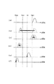
次に、センスラッチSLTの電源電圧SLP,SLNをリセット状態(SLP=SLN=0.5V)にして保持データを一旦キャンセル(図5のタイミングt3)した後、信号TRをハイレベルにしてデータ線上の伝送MOSFET Qt1をオンさせてデータ線の電位をセンスラッチSLTに伝えて(図5のタイミングt4)から、センスラッチSLTの電源電圧SLP,SLNを順バイアス状態にしてデータ線の電位を増幅する(図5のタイミングt5)。図6には上記信号タイミングに従ったときのセンスラッチSLTの入出力ノードとメインデータ線DLa,DLbの電位の変化を示す。
【0056】
なお、図6において、符号DAiはセンスラッチSLTのMATa(右側マット)側の入出力ノードNaの電位、符号DBiはセンスラッチSLTのMATb(左側マット)側の入出力ノードNbの電位、符号GDLAiはMATa側のメインデータ線DLaの電位、符号GDLBiはMATb側のメインデータ線DLbの電位である。また、図6(a)は選択メモリセルの現在の状態が書込み状態(低しきい値)である場合の波形、図6(b)は選択メモリセルの現在の状態が消去状態(高しきい値)で追加書込みでデータの書込みを行なわない場合の波形、図6(c)は選択メモリセルの現在の状態が消去状態(高しきい値)で追加書込みでデータの書込みを行なう場合の波形である。
【0057】
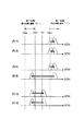
その後、図7に示すように、信号TRをロウレベルにして伝送MOSFET Qt1をオフさせてデータ線とセンスラッチSLTとを遮断した状態で、信号PC2A,PC2Bを立ち上げる(タイミングt6)。これによって、データ反転回路WRWa内のMOSFET Qp1がオンされてメインデータ線DLa,DLbがそれぞれ1V,0.5Vにプリチャージされる。次に、データ反転回路WRWa内の電源切替端子VPCをVssに切り替えてから信号PC1Aを立ち上げる(図7のタイミングt7)。
【0058】
すると、選択側ではデータ反転回路WRWa内のMOSFET Qp2がオンされるとともに、MOSFET Qt2がセンスラッチSLTの保持データに応じてそれが“1”のときはオンされ、“0”のときはオフとされる。そのため、センスラッチSLTの保持データが“1”に対応するメインデータ線DLaはVss(ロウレベル)にディスチャージされ、保持データが“0”に対応するメインデータ線DLaは1V(ハイレベル)のままにされる。つまり、データレジスタ12の保持データを反転した状態が選択側のデータ線上に現れる。
【0059】
次に、センスラッチSLTの電源電圧SLP,SLNをリセット状態にして保持データを一旦キャンセル(図7のタイミングt8)した後、信号TRをハイレベルにしてデータ線上の伝送MOSFET Qt1をオンさせてデータ線の電位をセンスラッチSLTに伝えて(図7のタイミングt9)から、センスラッチSLTの電源電圧SLP,SLNを順バイアス状態にしてデータ線の電位を増幅する(図7のタイミングt10)。これによって、データレジスタ12には、書込みを行なうべきメモリセルに対応したセンスラッチSLTにのみ“1”にされた書込み期待値データが保持される。この書込み期待値データは、追加書込みデータと既に書込みがなされたメモリセルの記憶データとを並べ反転させたものであることが、表1より容易に理解される。
【0060】
実施例のフラッシュメモリでは、上記書込み期待値データをデータレジスタ12に保持したまま、データ線上の伝送MOSFET Qt1をオフした状態で選択ワード線とウェル領域に消去パルスを印加して当該セクタのメモリセルをすべて消去状態(高しきい値)あるいは擬消去する。その後、データレジスタ12に保持されている上記書込み期待値データを用いて、保持データが“1”であるデータ線のみ3Vのようなレベルにプリチャージして選択ワード線に−10Vを印加することで、所望の追加書込みが実行される。その結果、プリチャージされなかったデータに接続されたメモリセルはしきい値が変化せず記憶データは“1”となり、逆にプリチャージされたデータに接続されたメモリセルはしきい値が低くされることで記憶データは“0”となる。
【0061】
なお、上記消去パルス印加時に消去状態であったメモリセルのしきい値は、最低限書込みベリファイ電圧を越えれば良く、消去時間の節約が可能である。
【0062】
図8には上記信号タイミングに従ったときのセンスラッチSLTの入出力ノードとメインデータ線DLa,DLbの電位の変化を示す。また、図8(a)は図5の動作終了時(タイミングt5)にセンスラッチSLTのマットA側の入出力ノードの電位がハイレベルであった場合のその後の波形、図8(b)は図5の動作終了時(タイミングt5)にセンスラッチSLTのマットA側の入出力ノードの電位がロウレベルであった場合のその後の波形を示す。
【0063】
図9には、各メモリセルの追加書込み前と追加書込み後のしきい値の変化の様子を示す。図9において、(A)は書込み前の状態が「消去(記憶データ“1”)」で追加書込みデータが“1”であるメモリセルの変化を、(B)は書込み前の状態が「消去(記憶データ“1”)」で追加書込みデータが“0”であるメモリセルの変化を、(C)は書込み前の状態が「書込み(記憶データ“0”)」で追加書込みがないメモリセルのしきい値の変化を示す。図9において、緩やかな右下がりの傾斜は、ディスターブによるしきい値の低下を意味している。なお、図9で破線で示すのは、初期書込みも追加書込みコマンドを用いて行なった場合のしきい値の変化である。即ち、メモリセルの一括消去直後の書込みにおいてもディスターブが起こるので、追加書込コマンドを用いる書込みは有効である。
【0064】
表2には、メモリセルの状態(記憶データ)と追加書込データおよび書込期待値データとの関係を示す。表2に記されているA,B,Cの符号は、図9のメモリセルのしきい値変化との対応を表すものである。
【0065】
【表2】
【0066】
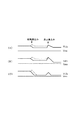
この実施例に従うと、図10(A-1),(B-1)に示すように、最初の書込み時のディスターブで破線で示すごとくしきい値が下がってしまっているメモリセルのしきい値を回復してやることができる。前述の説明では詳しく述べなかったが、1セクタを一括消去して、その中の特定のメモリセル群に書込みを行うと、残りのメモリセルは最初からワードディスターブを受けるのである。なお、図10において、(A-1),(A-2)は同一セクタ内でしきい値電圧が第1状態にある未使用領域の第1メモリセル群(消去状態)に書込みを行なわない場合のしきい値の変化の様子を、(B-1),(B-2)は同じく第1メモリセル群に書込みを行なう場合のしきい値の変化の様子を示す。また、(C-1),(C-2)は使用領域にあるしきい値電圧が第2状態の書込み状態の第2メモリセル群のしきい値の変化の様子をそれぞれ示す。同図から分かるように、この実施例では書込み済みのメモリセルも一旦消去状態にされてから再び書込み状態とされる。
【0067】
なお、上記実施例では、セクタを使用領域と未使用領域の2つに分けた場合について説明したが、それに限定されるものでなく、上記未使用領域を複数のセクションに分割して各セクションごとに追加書込みを可能な構成にしてもよい。
【0068】
さらに、上記実施例では、データ書込みの際に一旦消去を行なってしきい値を高くした後に書込みパルスでしきい値を下げる方式のフラッシュメモリについて説明したが、消去動作でメモリセルのしきい値を低くしてから書込みパルスでしきい値を高くする方式等であっても良い。
【0069】
図1に示した1チップに形成された第1の実施例のフラッシュメモリは、上述した追加書込みコマンド(第2書込みコマンド)の他に、少なくとも、図13の読出しコマンド、図14の消去コマンド(1セクタのメモリセルのしきい値電圧を一括して第1状態(消去状態)にするコマンド)、図15の書込みコマンド(第1書込みコマンド)を有する。図13〜14の手順の詳細は後に説明する。消去コマンドを実行して1セクタ内でしきい値が第2状態にあるメモリセル群を第1状態にするには、約1msの時間を要する。書込みコマンドを実行してしきい値が第1状態にあるメモリセル群を第2状態にするには同じく約1msの時間を要する。
【0070】
以上の実施例により達成される本願発明の作用効果は以下の通りである。まず、図4の追加書込みコマンドと図15の書込みコマンドとを比較すると、追加書込みコマンドは、ステップ4−5(S4−S5)の手順が特徴となる。ステップ4により最終書込みデータの合成が自動的に行われるようになり、書込み時間の節約となる。
【0071】
また、しきい値電圧の電圧方向を特徴的に決めるワード線への電圧印加で比較すると、図14の消去コマンドでは+10Vのみが約1ms印加されるステップを含み、図15の書込みコマンドでは−10Vのみが約1ms印加されるステップを含む。これに対し、図4では+10Vに引き続き−10Vを印加するステップを有することで特徴付けられる。また、ステップ5の擬消去で+10Vを印加する時間は、消去コマンドで+10Vを印加する時間より大幅に短くされることで特徴付けられる。
【0072】
ディスターブを回避するために1セクタの書込みデータを一旦センスラッチSLTに退避してメモリセルを消去コマンドで完全に一括消去(約1ms)した後、センスラッチSLTに退避したデータと新たな書込みデータから合成した最終書込みデータを書込みコマンドでメモリセルへ書込みを行う(約1ms)方法では、合計約2ms以上の時間を要する。これに対して、図23で示すような擬消去を用いた追加書込みコマンドによれば、擬消去(約0.1ms)の後、書込み(約1ms)となるので、トータル約1.1msで完了し、実質的な書込み時間を約半分とすることができる。
【0073】
また、擬消去によりディスターブの補償がなされワードディスターブが緩和されるため、追加書込みコマンドでは、実行に先立ち消去コマンドを実行して完全なセクタ消去をしなくてもよい。即ち、従来の書込みコマンドでは、その実行に先立ち消去コマンドを実行しなければならない制約があった。これに対し、追加書込みコマンドでは、ディスターブが大幅に緩和されるため、消去コマンドを実行せずに連続して実行できる回数を大幅に増やすことができる。つまり、本願発明の追加書込みコマンドは、消去コマンドを実行せずに、約15回以上連続して実行しても、同一セクタ内のメモリセルの記憶データが保証される。消去−書込みを15回以上繰り返すと30msとなるのに対し、追加書込みコマンドを15回連続して実行して1回消去コマンドを実行すると、17.5msとなるに過ぎず、システム全体としても書込み時間が大幅に節約される。
<実施例2>
図11には、上記書込みパルスでしきい値を高くする方式のメモリアレイの実施例を示す。
【0074】
この実施例のメモリアレイと前記実施例のメモリアレイ(図2参照)との相違は、選択MOSFET Qs1,Qs2がなく各メモリセルMC1〜MCnのドレインが直接メインデータ線DLに接続されているとともに、各メモリセルMC1〜MCnのソースは共通のコモンソース線CSLに接続されている点にあり、同一列のメモリセルは互いに並列的に接続されている点では前記実施例のメモリアレイと同じである。ただし、この実施例のメモリアレイでは、データ書込み時と消去時のメモリセルのしきい値電圧の定義が図2の実施例と逆である。
【0075】
特に制限されないが、図11に示すメモリアレイはNOR形フラッシュメモリと呼ばれることがある。この時、特に制限されないが、フローティングゲートへの電子の注入(しきい値電圧を上げ、書込み状態にする)には、トランジスタのドレインからCHE(Channel Hot Electron)注入が用いられ、フローティングゲートからの電子の引き抜き(しきい値電圧を下げ、消去状態にする)には、FNトンネル放出が用いられる。
【0076】
この実施例では、表3に示すように、データ書込み時にはコントロールゲートCGに10Vのような高電圧が印加され、ソースには接地電位(0V)が印加される。一方、ドレインには、選択/非選択に応じて異なる電圧が印加される。すなわち、選択メモリセルのドレインには5Vのような電圧が印加されてメモリセルはオン状態となり、ソース・ドレイン間に電流が流れこのとき生じたホットエレクトロンがフローティングゲートに注入されてメモリセルのしきい値が高くされる。また、非選択メモリセルのドレインにはソースと同じ0Vが印加されてメモリセルのソース・ドレイン間には電流が流れずメモリセルのしきい値も低いままとされる。
【0077】
【表3】
【0078】
この実施例においても、前記実施例と同様な追加書込み制御を適用することにより、図12(A-1),(B-1)に示すように、最初の書込み時のディスターブで破線で示すごとくしきい値が上がってしまっているメモリセルのしきい値を回復してやることができる。なお、図12において、(A-1),(A-2)は未使用領域のメモリセル(消去状態)に書込みを行なわない場合のしきい値の変化の様子を、(B-1),(B-2)は未使用領域のメモリセルに書込みを行なう場合のしきい値の変化の様子を、(C-1),(C-2)は使用領域にある書込み状態のメモリセルのしきい値の変化の様子をそれぞれ示す。同図から分かるように、この実施例では書込み済みのメモリセルも一旦消去状態にされてから再び書込み状態とされる。
【0079】
図24に示されるように、メモリセルのしきい値の変化を電圧Vpvよりもわずかに低くする程度であってもよい。
【0080】
以上本願の実施例2を用いて、第1状態と第2状態のしきい値電圧の高低を逆にしても実施例1と同様な効果が得られる。
<実施例3>
図13〜図15に本発明の他の実施例を示す。この実施例は、前記実施例における追加書込みコマンドや書込み期待値データ機能をフラッシュメモリに持たせずに、外部の制御装置からの一般的なデータ読出しコマンドと消去コマンドと書込みコマンドによって追加書込みを実行するようにしたものである。この実施例を適用できるフラッシュメモリは、少なくともデータ読出しコマンドと消去コマンドと書込みコマンドと開始コマンドとを解読して実行するシーケンサを備えている。このうち開始コマンドは必ずしも必要とされるものでなく、自動的にスタートするように構成することができる。
【0081】
即ち、不揮発性メモリとしては、メモリアレイとシーケンサとが1チップ上に形成され、シーケンサは少なくとも、読出しコマンド(図13)、消去コマンド(図14)および書込みコマンド(図15)の基本命令を実行可能とされている。そして、実施例1で説明したように完全な一括消去と前述の擬消去とができるように、消去コマンドでのワード線の電圧印加時間や実行ステップは、変更可能にできるものとする。擬消去専用に消去時間だけが異なる第2消去コマンドを設けてもよい。また、この時、消去コマンドの消去ベリファイは不要とされる。
【0082】
本願発明の追加書込みコマンドは、上記3つの基本命令を順次連続して実行するマクロコマンドとなり、そのコマンドは例えばパーソナルコンピュータのCPUで実行可能なプログラムとして、磁気記憶媒体等により配布可能とされる。従って、この場合のシーケンサは、メモリチップの狭義のシーケンサと外部のCPUとが一体となったものである。追加コマンドの形態としては、不揮発性メモリドライバとして追加プログラムされたり、しばしばコンピュータのOSに組み込まれる形式とされる。従って、本願の対象は、3個の基本命令が実行できる不揮発性メモリチップと、それが接続されるCPUを持つコンピュータシステムの一部となり得る。
【0083】
以下、図13〜図15に従って、本実施例を説明する。
【0084】
本実施例においては、追加書込みをする場合、外部の制御装置からフラッシュメモリに対して先ずデータ読出しコマンドが入力され、続いてデータを追加書込みしたい位置に相当するセクタアドレスが入力される。フラッシュメモリは、データ読出しコマンドが入力されると、メモリ内部の各回路を読出しモードに設定する(図13のステップS11)。続いてアドレスが入力されるとそのアドレスをアドレスレジスタに格納する(ステップS12)。次に、外部から開始コマンドが入力されると、上記アドレスレジスタに格納されたアドレスのデータをメモリアレイ内から読み出して外部へ出力する。外部の制御装置は、フラッシュメモリから出力されたデータを外部のメモリ内の所定の退避エリアに格納する。また、外部制御装置は上記退避エリアに格納された読出しデータと追加書込みデータとから書込み期待値データを作成して外部メモリに保持しておく。
【0085】
次に、外部制御装置からフラッシュメモリに対して消去コマンドとセクタアドレスが入力される。すると、フラッシュメモリはメモリ内部の各回路を消去モードに設定してから、入力されたアドレスをアドレスレジスタに格納する(図14のステップS21,S22)。続いて開始コマンドが入力されると、上記アドレスレジスタに設定されたセクタアドレスに対応するメモリセルに対して、消去状態あるいは擬消去状態にするためのバイアス電圧を印加してしきい値を変化させる(ステップS23)。その後、ベリファイ読出しを行なって、確実にデータが消去されたか確認し、消去がなされていないときはステップS23へ戻って再度メモリセルに対して消去パルスを印加する(ステップS24,S25)。なお、ステップS22〜25の消去ベリファイは、通常の消去時に利用され、擬消去では使用されない。
【0086】
次に、外部制御装置からフラッシュメモリに対して書込みコマンドとセクタアドレスおよび書込み期待値データが順次入力される。すると、フラッシュメモリはメモリ内部の各回路を書込みモードに設定してから、入力されたアドレスをアドレスレジスタに、また書込み期待値データをデータレジスタに格納する(図15のステップS31,S32,S33)。続いて開始コマンドが入力されると、上記アドレスレジスタに設定されたセクタアドレスに対応するメモリセルに対して、書込みパルスを印加してしきい値を変化させる(ステップS34)。その後、ベリファイ読出しを行なって、確実にデータの書込みがなされたか確認し、書込みがなされていないときはステップS34へ戻って再度メモリセルに対して書込みパルスを印加する(ステップS35,S36)。
【0087】
以上、読出しコマンド、消去コマンドおよび書込みコマンドの3個の基本命令の組み合わせにより作ったマクロ追加書込みコマンドについて説明したが、図4の実施例に比べると、読出しデータをメモリチップ外部に取り出すため、図4のステップS4に対する手順の節約効果は薄れるものの、ワードディスターブを回避し、消去命令を実行せずにできる追加書込みについては実施例1と同様な効果が期待できる。
【0088】
図16には、本発明の更に他の実施例を示す。図1と同一の符号については、その詳細な説明は省略する。この実施例は、上記実施例における退避エリアとなるレジスタ(データ退避レジスタ)27と、外部制御装置が行なっている書込み期待値データの演算を行なう演算回路(追加書込み対応演算回路)28とをフラッシュメモリ内部に設けるようにしたものである。この実施例のシーケンサ22は外部の制御装置から入力される追加書込みコマンドを解読して、上記レジスタ27および演算回路28を適当なタイミングで制御して追加書込みを実行させる機能を有するように構成される。
【0089】
図17には上記実施例のフラッシュメモリの応用例としてのメモリカードの構成を示す。メモリカード100は、複数のフラッシュメモリ10とこれらのリード・ライトを制御するコントローラユニット110とによって構成されており、コントローラユニット110とフラッシュメモリ10とは、カード内に配設されたバス(図示省略)によって接続されており、コントローラユニット110からフラッシュメモリ10に対して、上述の追加書込みコマンドその他のコマンドやセクタアドレス、書込みデータ、ライトイネーブル信号などの制御信号がバスを介して供給される。120は、カードの一側に沿って設けられた信号入出力や電源供給用の端子兼コネクタである。
【0090】
実施例1や実施例2では、フラッシュメモリのメモリアレイと、命令を実行するためのコマンドシーケンサが1チップ上に設けられた不揮発性メモリについて述べたが、その実現方法は、図17のようにカード形とすることもできる。このとき重要なことは、コントローラ110が少なくとも、図4で示した追加書込みコマンドの手順を含む不揮発性メモリシステムを構成することである。
【0091】
メモリカード形態としたときの別の実施例としては、コントローラ110を省略し、フラッシュメモリチップが複数搭載されたメモリカードと、これらのメモリカードが接続可能とされるCPUを含むパーソナルコンピュータの形態も取り得る。この場合には、フラッシュメモリの制御に必要な消去、書込み等の全てのコマンドはCPUのプログラムとして含まれることとなる。そして、そのコマンドには図4の追加書込みコマンド、または図13〜15の基本命令を組み合わせたマクロ書込みコマンドを用いることができる。
【0092】
以上説明したように、上記実施例においては、所定の指令が与えられると、指定アドレスのセクタの記憶データを読み出してレジスタに退避させてから当該セクタの一括消去を行ない、前記退避されたデータと追加書込みしようとするデータとから実際の最終書込みデータ(書込み期待値データ)を形成して書込み動作を行なうように構成したので、追加書込みの際にワード線ディスターブによるメモリセルのしきい値の変動が回復され、誤まったデータの読み出しを防止することができるという効果がある。
【0093】
また、選択セクタから読み出されたデータを内部レジスタに保持した状態で外部から追加書込みデータが入力されると、書込み期待値データを自動的に内部で形成してから書込み動作を行なうように構成したので、追加書込みという動作を通常の書込みよりも高速で行なうことができ、しかも追加書込みにおけるソフトウェアの負担を軽減することができるという効果がある。
【0094】
その結果、実施例のフラッシュメモリによれば、図22に示すように、同一セクタ内にOS情報やセクタ管理情報等一般ユーザーに開放されていないシステム領域と、一般ユーザーが自由に書込みをできるユーザー領域とを混在して設けることができ、これによってメモリの有効利用を図かることができる。このような記憶方式のフラッシュメモリは、システム領域に所定のデータが書き込まれ、ユーザー領域は未書込みの状態でユーザーに提供され、ユーザーが書込みを行なう時は追加書込みという動作で行なえるためである。なお、図22における管理データとしては、例えばパリティコードやエラー訂正符号、当該セクタの書換え回数、等がセクタが不良ビットを含むか否かの情報、当該セクタを複数のセクションに分割して各セクションごとに追加書込みを可能な構成にした場合におけるセクションの使用/未使用を示すセクション管理情報等がある。
【0095】
以上本発明者によってなされた発明を実施例に基づき具体的に説明したが、本発明は上記実施例に限定されるものではなく、その要旨を逸脱しない範囲で種々変更可能であることはいうまでもない。例えば、上記実施例では、メモリアレイを2つのマットによって構成した場合について説明したが、この発明はそれに限定されず、偶数個のマットに分割した場合はもちろん1つのマットで構成されている場合にも適用することができる。
【0096】
以上の説明では主として本発明者によってなされた発明をその背景となった利用分野である一括消去型フラッシュメモリに適用した場合について説明したが、この発明はそれに限定されるものでなく、FAMOSを記憶素子とする不揮発性記憶装置一般さらには複数のしきい値を有するメモリセルを備えた半導体装置に広く利用することができる。
【0097】
【発明の効果】
本願において開示される発明のうち代表的なものによって得られる効果を簡単に説明すれば下記のとおりである。
【0098】
すなわち、この発明は、不揮発性半導体記憶装置におけるワード線ディスターブによるメモリセルのしきい値の変動を回復し、誤まったデータの読み出しを防止することができるとともに、追加書込みという動作を通常の書込みよりも高速で行なうことができ、しかも追加書込みにおけるソフトウェアの負担を軽減することができる。
【図面の簡単な説明】
【図1】本発明に係るフラッシュメモリの一実施例の概略を示す全体ブロック図である。
【図2】本発明に係るフラッシュメモリのメモリアレイの構成例を示す回路図である。
【図3】センスラッチ回路SLTおよびデータ反転回路WRWの具体例を示す回路図である。
【図4】実施例のフラッシュメモリの追加書込み手順を示すフローチャートである。
【図5】実施例のフラッシュメモリにおける追加書込み時(前半)のメモリアレイ内の信号タイミングを示すタイミングチャートである。
【図6】実施例のフラッシュメモリにおける追加書込み時(前半)のセンスラッチおよびデータ線のレベル変位を示す波形図である。
【図7】実施例のフラッシュメモリにおける追加書込み時(後半)のメモリアレイ内の信号タイミングを示すタイミングチャートである。
【図8】実施例のフラッシュメモリにおける追加書込み時(後半)のセンスラッチおよびデータ線のレベル変位を示す波形図である。
【図9】実施例のフラッシュメモリにおける追加書込み時のメモリセルのしきい値の変化を示す説明図である。
【図10】実施例のフラッシュメモリにおけるメモリセルのしきい値の変化を示す説明図である。
【図11】本発明に係るフラッシュメモリのメモリアレイの他の実施例を示す回路図である。
【図12】図11の実施例のフラッシュメモリにおけるメモリセルのしきい値の変化を示す説明図である。
【図13】本発明に係るフラッシュメモリの第2の実施例を説明する第1ステージの読出しコマンド実行手順を示すフローチャートである。
【図14】本発明に係るフラッシュメモリの第2の実施例を説明する第2ステージの消去コマンド実行手順を示すフローチャートである。
【図15】本発明に係るフラッシュメモリの第2の実施例を説明する第3ステージの書込みコマンド実行手順を示すフローチャートである。
【図16】本発明に係るフラッシュメモリの第3の実施例の概略を示す全体ブロック図である。
【図17】本発明に係るフラッシュメモリの応用例としてのメモリカードの概略構成図である。
【図18】フラッシュメモリにおけるメモリセルの書込み時の印加電圧の一例を示す断面図である。
【図19】フラッシュメモリにおけるメモリセルの消去時の印加電圧の一例を示す断面図である。
【図20】従来のフラッシュメモリにおけるメモリセルのしきい値の変化を示す説明図である。
【図21】従来の他のフラッシュメモリにおけるメモリセルのしきい値の変化を示す説明図である。
【図22】フラッシュメモリにおける追加書込み可能なセクタの構成例を示す説明図である。
【図23】実施例のフラッシュメモリにおけるメモリセルのしきい値の変化を示す他の説明図である。
【図24】図11の実施例のフラッシュメモリにおけるメモリセルのしきい値の変化を示す他の説明図である。
【符号の説明】
11 メモリアレイ
12 データレジスタ
13 書換回路
14 アドレスレジスタ
15 Xデコーダ
21 コマンドレジスタ&デコーダ
22 シーケンサ
SLT センスラッチ回路
WRWデータ反転回路
DL データ線
WL ワード線
MC メモリセル[0001]
BACKGROUND OF THE INVENTION
The present invention relates to a technique that is particularly effective when applied to an information writing method in a semiconductor memory device and further a nonvolatile semiconductor memory device. For example, a nonvolatile memory system and a nonvolatile semiconductor memory capable of electrically erasing a plurality of stored information collectively It is related to effective technology.
[0002]
[Prior art]
A flash memory uses a nonvolatile memory element having a control gate and a floating gate as a memory cell, and can constitute a memory cell that stores a threshold voltage as information with a single transistor (MOSFET). In such a flash memory, in the write operation, as shown in FIG. 18, the drain voltage of the nonvolatile memory element is set to 5 V (volt), for example, and the word line connected to the control gate CG is set to -10 V, for example. Electric charges are extracted from the floating gate FG to the drain region, and the threshold voltage is lowered (logic “0”). In the erase operation, as shown in FIG. 19, the well region is set to −5V, for example, the control gate CG is set to a high voltage such as 10V, and negative charges are injected into the floating gate FG to increase the threshold (logic “ 1 "). Thereby, 1-bit data is stored in one memory cell.
[0003]
[Problems to be solved by the invention]
In a conventional flash memory, control gates of a plurality of memory cells are connected to one word line, and a plurality of memory cells connected to the word line are defined as units (hereinafter referred to as sectors), Writing and reading have been performed with distinction between the respective operation modes. First, erasing is simultaneously performed on a plurality of memory cells sharing a word line. This erasing is performed in units of sectors, and it is not possible to selectively erase only a specific memory cell among a plurality of memory cells.
[0004]
On the other hand, in programming, after erasing and raising the threshold as shown in FIG. 20A, -10 V is applied to the word line connected to the memory cell to be lowered and the drain is applied. 5V and 0V were applied to the source. As a result, the threshold value of the memory cell to which data has been written becomes lower than the verify voltage Vpv as shown in FIG. At this time, 0V is applied to the drain of the memory cell where writing is not performed, that is, the threshold value is not lowered, but -10V is applied to the gate of the other memory cell sharing the word line with the writing cell. Since such a large voltage is applied, a phenomenon occurs in which the threshold value slightly decreases. Although it is desirable that only the threshold voltage of a specific memory cell to be written changes, a slight change in the threshold value also occurs in a memory cell to which writing is not performed. This undesirable threshold voltage change is called disturb. Such a disturb phenomenon is mainly caused by applying a voltage to the word line, and is therefore called word line disturb (or word disturb).
[0005]
Due to the above-described word disturb, it is difficult to repeatedly write the memory cells in units of sectors without performing batch erasure. This state is shown in FIGS. 20 (c) to 20 (f). When a plurality of memory cells connected to the same word line are erased at a time, the threshold values of the plurality of memory cells all become the highest erase level (FIG. 20A). Next, writing is performed, and a threshold value of a specific memory cell is selectively set to a writing state (FIG. 20B). At this time, the plurality of memory cells include a first memory cell group in which the threshold voltage is in the erased state (dotted line in FIG. 20C) and a second memory cell group in which the threshold voltage is in the written state (see FIG. d) dotted line). Since selective memory cells cannot be erased, writing can be performed only to the first memory cell. Therefore, writing is performed by selecting one of the first memory cell groups. At this time, when word disturb occurs, the threshold voltage of the memory cell that has not been written decreases as shown in FIGS.
[0006]
If the disturb is repeated several times by repeating the writing without performing the batch erase, the threshold value of the memory cell becomes lower than the word line level Vr at the time of data reading as shown in FIG. Incorrect data is read out. Further, as shown in FIG. 20 (f), when it is lower than the ground potential Vss and is in the non-selected state, it is turned on, and when a memory cell having a different word line but a common source line is selected, Since the charges on the line flow to the source through the memory cell having a threshold value lower than the ground potential Vss, there is a problem that erroneous data reading may be performed.
[0007]
Depending on the configuration of the memory array, there is a method in which the low threshold state is set to the erased state and the threshold value of the memory cell is increased by writing. However, even in such a writing method, the word line is shared. There is a disturb phenomenon in which the threshold value of a non-written memory cell becomes slightly higher (see FIGS. 21C and 21D). If the disturb is repeated several times, the threshold value of the memory cell becomes higher than the word line level Vr at the time of data reading as shown in FIG. is there.
[0008]
FIG. 22 shows an information mat of sectors managed by one word line. For example, in FIGS. 20A-1 to 20A-3, 512 byte (4096 bit) memory cells are connected to one word line. Here, as shown in FIG. 22, a storage area that is not open to general users (hereinafter referred to as a system area) such as OS information (operation system information) and sector management information in the same sector, and free for general users. A memory area (hereinafter referred to as a user area) that can be written to is provided in a mixed manner, so that the memory can be effectively used. In practice, the system area is very small compared to the user area. In such a storage type flash memory, predetermined data is written in the system area, and the user area is provided to the user in an unwritten state. It is convenient to perform an operation called additional writing in which a memory cell in the erased state of a user area having a large information area is selected and repeatedly written. However, in the system using the conventional flash memory, such additional write operation has not been performed because the stored information cannot be guaranteed due to the disturbance. Further, even if additional writing is permitted, it is necessary to greatly limit the number of times of additional writing in succession in consideration of threshold fluctuation due to disturbance.
[0009]
Further, the memory itself has not been designed in consideration of the above usage. Therefore, if additional writing is performed with a conventional flash memory, the same algorithm as normal writing, that is, the sector data is once read to the outside and the sector is collectively erased, and then the read data and additional write data are It has become clear that there is a problem that the time required for additional writing becomes very long and the burden of software becomes large because writing must be performed by combining.
[0010]
An object of the present invention is to provide a non-volatile memory system and a non-volatile semiconductor memory capable of recovering fluctuations in the threshold value of a memory cell due to word line disturbance.
[0011]
Another object of the present invention is to provide a nonvolatile memory system and a nonvolatile semiconductor memory capable of continuously executing additional writing without performing batch erasure.
[0012]
Another object of the present invention is to provide a non-volatile memory system and a non-volatile semiconductor memory capable of performing the operation of additional writing at a higher speed than normal writing and reducing the burden of software in the additional writing. There is to do.
[0013]
The above and other objects and novel features of the present invention will be apparent from the description of this specification and the accompanying drawings.
[0014]
[Means for Solving the Problems]
The following is a brief description of an outline of typical inventions disclosed in the present application.
[0015]
That is, when a predetermined command is given, the stored data of the sector at the designated address is read out and saved in a register, and then the sector is erased collectively, and the actual data is calculated from the saved data and the data to be additionally written. Write data (hereinafter referred to as write expected value data) is formed and a write operation is performed.
[0016]
A plurality of memory cells for storing information in a first state (for example, an erased state having a high threshold voltage) and a second state (for example, a written state having a low threshold voltage); A memory array having a word line connected to a control gate of the memory cell, and a command input terminal, and an erase and write operation of the plurality of memory cells in accordance with a command input to the command input terminal according to a predetermined procedure A sequencer controlled according to the sequencer, the command received by the sequencer includes an erase command for collectively changing a threshold voltage of a plurality of memory cells to a first state, and a threshold value of the plurality of memory cells An additional write command for selectively changing at least one of the memory cells having a voltage in the first state to the second state, De, constituting the nonvolatile memory system as multiple times consecutively without executing the erase command is executable to write the data.
[0017]
Further, in a preferred embodiment, among the plurality of memory cells, a memory cell having a threshold voltage in a first state is defined as a first memory cell group, and a memory cell having a threshold voltage in a second state is defined as a memory cell. When the second memory cell group is set, the sequencer sets the threshold voltage of the second memory cell group between the first state and the second state when the additional write command is input. After performing the first step, at least one of the first memory cell groups is selectively set to the second state, and the threshold voltage of the memory cells of the second memory cell group is set to the second state. Configured to perform a second step.
[0018]
Furthermore, in another preferred embodiment, the instruction received by the sequencer includes an erase command for collectively changing a threshold voltage of a plurality of memory cells to a first state, and the plurality of memory cells. A first write command including a step of applying a second voltage to the word line to change a threshold voltage of the selected first memory cell group to the second state; and After the first voltage is applied to the word line in order to change the threshold voltage in the voltage direction from the second state to the first state, the selection of the selected second memory cell group included in the plurality of memory cells is performed. A second write command including a step of applying a second voltage to the word line in order to change the threshold voltage to the second state.
[0019]
As a result, the fluctuation of the threshold value of the memory cell due to the word line disturbance is recovered at the time of additional writing, and erroneous data reading can be prevented. As a result, it is possible to greatly increase the number of times that additional writing can be continuously executed without executing the erase instruction.
[0020]
In addition, using the data read from the selected sector and held in the internal register and the additional write data input from the outside, the write expected value data is automatically formed internally before the write operation is performed. As a result, the operation of additional writing can be performed at a higher speed than normal writing, and the burden of software on additional writing can be reduced.
[0021]
DETAILED DESCRIPTION OF THE INVENTION
Hereinafter, an embodiment in which the present invention is applied to a flash memory will be described with reference to the drawings.
<Example 1>
FIG. 1 shows an embodiment of a flash memory to which the present invention is applied. Although not particularly limited, each circuit block shown in FIG. 1 is formed on one
[0022]
In FIG. 1,
[0023]
[0024]
The flash memory of this embodiment has a data input / output interface for serial access, although not particularly limited. For example, at the time of reading, when an address of a sector to be read is input, one word line is selected, and data is read in parallel from a plurality of memory cells connected thereto, and each is read into a sense latch group SLT described later. Once held. This sense latch group is included in the data register 12. The sense latch groups are sequentially selected by the
[0025]
The flash memory of this embodiment is not particularly limited, but holds a command given from an external CPU or the like, decodes the command, and the command based on the decoding result of the command register &
[0026]
The
[0027]
Furthermore, in addition to the above circuits, the flash memory of this embodiment has an I /
[0028]
Although not particularly limited, the flash memory of this embodiment shares an external terminal (pin) I / O for an address signal, a write data signal, and a command input. Therefore, the I /
[0029]
The control signal input from the external CPU or the like to the flash memory of this embodiment indicates, for example, a reset signal RES, a chip selection signal CE, a write control signal WE, an output control signal OE, a command or data input, or an address input. There are a command enable signal CDE, a system clock SC and the like.
[0030]
As an external device for controlling the flash memory of the above embodiment, a general-purpose microcomputer LSI can be used as long as it has an address generation function and a command generation function.
[0031]
FIG. 2 shows a specific example of the
[0032]
Although not particularly limited, the system having the configuration of the memory array shown in FIG. 2 and taking the erase state at a high threshold voltage and taking the write state at a low threshold voltage may be called an AND flash memory. In this case, electron injection into the floating gate (threshold voltage is increased to make the erase state) is not particularly limited, but FN (Fowler-Nordheim) tunnel injection is used from the channel of the transistor, and from the floating gate. FN tunnel emission to the diffusion layer is used for extracting electrons (lowering the threshold voltage and setting the write state).
[0033]
When data is erased, a negative voltage such as −3V is applied to the well region WELL and the local source line LSL, and a voltage such as 10V is applied to the word line sharing the well region, thereby enabling batch erase. Yes. Note that at the time of data erasure, the selection MOSFET Qs2 is turned on, and a negative voltage of −3 V is applied to the source of each memory cell. At this time, the selection MOSFET Qs1 is turned off, and the drain is supplied with a voltage on the source side through the channel of the memory cell which is turned on by applying a high voltage of 10V to the control gate. Potential.
[0034]
On the other hand, at the time of data writing, a negative voltage such as −10V is applied to the word line to which the selected memory cell is connected, and the main data line DL corresponding to the selected memory cell is set to a potential such as 3V. The selection MOSFET Qs1 on the local data line LDL to which the selected memory cell is connected is turned on, and 3 V is applied to the drain. However, at this time, the selection MOSFET Qs2 on the local source line LSL is in an OFF state.
[0035]
At the time of data reading, a voltage such as a read voltage Vr (for example, 2.0 V) is applied to the word line to which the selected memory cell is connected, and the main data line DL corresponding to the selected memory cell is applied. The selection MOSFET Qs1 on the local data line LDL precharged to a potential such as 1V and connected to the selected memory cell is turned on. At this time, the selection MOSFET Qs2 on the local source line LSL is turned on, and the ground potential (0 V) is applied. This distinguishes between the case where the current flows according to the threshold voltage of the memory cell (the LDL potential is reduced to 0V) and the case where the current does not flow (the LDL potential is maintained at 1V). The stored information is read out.
[0036]
Here, the voltage at the time of data writing and erasing is lower than that of the conventional type shown in FIGS. 18 and 19 because the element size is reduced by using a technique capable of fine processing as compared with the conventional type and the power supply voltage Vcc is used. This is because 3V is used instead of the conventional 5V.
[0037]
One end of the main data line DL (at the center of the memory array) detects the level of the data line at the time of reading and supplies a sense latch circuit SLT for applying a potential corresponding to the written data at the time of writing and expected value data at the time of additional writing. The data inversion circuits WRW used for forming are connected to each other. The set of the sense latch circuits SLT is the data register 12 in FIG. 1, and the set of the data inversion circuits WRW is the
[0038]
In this embodiment, the memory array is composed of two memory mats, and the data inverting circuit WRW and the memory mat are arranged on the opposite side of the sense latch circuit SLT, that is, on the lower side of the figure. The data line DL is connected to the other input / output terminal of the sense latch circuit SLT via the corresponding data inverting circuit WRW. That is, the data inverting circuit WRW is provided for each of the mats MATa and MATb (referred to as WRWa and WRWb for distinction), and the sense latch circuit SLT is shared by the two memory mats.
[0039]
FIG. 3 shows specific circuit examples of the sense latch circuit SLT and the data inverting circuit WRW. Since the circuit is symmetrical with respect to the sense latch circuit, only one data line in one memory mat is illustrated, and for convenience, only one memory column MCC is shown among the memory columns connected to the data line. However, actually, a plurality of memory columns MCC are connected. As shown in the figure, the sense latch circuit SLT is composed of a flip-flop circuit FF in which input / output terminals of two CMOS inverters composed of a P-channel MOSFET and an N-channel MOSFET are cross-coupled. The pair of input / output terminals Na and Nb of the sense latch circuit SLT are connected to column switch MOSFETs Qya and Qyb constituting a so-called Y gate which is controlled to be turned on and off by the output of the Y decoder. The other ends of the plurality of column switches Qya and Qyb provided for each main data line are commonly connected to complementary common input / output lines (IO, / IO).
[0040]
The data inverting circuit WRWa includes a transmission MOSFET Qt1 connected between one input / output terminal Na of the sense latch circuit SLT and a main data line DLa in one memory mat, a power supply voltage terminal Vcc, and a main data line DLa. And a precharge MOSFET Qp1 controlled by a control signal PC2A, and MOSFETs Qt2 and Qp2 connected in series between the precharge switching terminal VPC and the main data line DLa. Among them, the potential of the input / output terminal Na of the sense latch circuit SLT is applied to the gate of Qt2, and the control signal PC1A is applied to the gate of Qp2. The precharge switching terminal VPC is configured to be supplied with a power supply voltage Vcc or Vss.
[0041]
Further, a data inverting circuit WRWb including MOSFETs Qt1, Qt2, Qp1, and Qp2 having the same configuration is connected to the other input / output terminal Nb of the sense latch circuit SLT.
[0042]
FIG. 4 shows a control procedure when data is additionally written by the
[0043]
This control sequence is started when an additional write command is taken into the command register &
[0044]
Next, when a write start command is taken into the command register &
[0045]
Subsequently, an erase pulse of 10V is applied to the selected word line and -3V is applied to the well region to raise the threshold values of all the memory cells in the sector (step S5). This step is one of the features of the present application. As a result, the memory cell in which the stored data is logical “0” has a threshold value of Vev or more as shown in FIG. 10C-1, the stored data changes to logical “1”, and the stored data is logically “1”. The disturbance of the memory cell which is 1 ″ is recovered as shown in FIG. It should be noted that the memory cell disabling in which the stored data is logic “1” occurred when writing to another memory cell in the same sector.
[0046]
Step S5 in FIG. 4 is an example in which the threshold values of all the memory cells in the sector are made higher than the voltage Vev. However, the present invention is not limited to this, and FIG. 23 (c-1) As described above, the threshold value of the memory cell in which data is already written in the sector may be set higher than the voltage Vpv (<Vev). For the sake of convenience, the operation of bringing the memory cells in the same sector to a higher potential side than the voltage Vpv without making the threshold voltage higher than the voltage Vev collectively is called pseudo-erasure. This pseudo-erasure is distinguished by the voltage application time although the voltage applied to the memory cell is the same as compared with the operation of erasing the memory cells of one sector at a time. That is, in order to execute an erase command described later with reference to FIG. 14 to completely erase a memory cell in the written state, 10 V is normally applied to the selected word line for 1 ms. On the other hand, in pseudo erasure, the time is about 1/10 (about 0.1 ms).
[0047]
Accordingly, the threshold voltage of the first memory cell group in which the threshold voltage is in the second state within one sector does not completely change to the first state, but the threshold voltage is the first threshold voltage. It is set to an intermediate level between the first state and the second state. In addition, the second memory cell group which is the remaining of the first memory cell group in the same sector and has the threshold voltage in the first state has a voltage direction in which the threshold voltage further increases (that is, the threshold voltage of the first threshold voltage). The threshold voltage is changed in the voltage direction from the second state to the first state. In other words, pseudo-erasing is not complete erasing of the memory cell, but reverses the amount of the threshold voltage in the voltage direction from the first state to the second state caused by word disturb and canceling the change in advance. It can be considered that the threshold voltage is changed in the voltage direction.
[0048]
Next, the selected word line is set to -10V, and the data line is set to 3V using the expected value data created in step S4 and held in the data register 12 (sense latch SLT). Is selectively set to write (step S6). The voltage level of the local data line LDL of the memory cell not to be written is set to 0V. Then, reading is performed using the verify voltage Vpv, and it is checked whether or not the threshold value is sufficiently low by determining whether or not all the data held in the data register 12 is “0” (step S7). If at least one “1” data remains, it is determined that there is a memory cell having a high threshold value, and the process returns to step S6 to rewrite using the data held in the data register 12 at that time. Repeat the verification.
[0049]
In the above repeating process, the memory cell whose threshold value is already sufficiently low (threshold voltage is lower than the verify voltage Vpv) is set so that the voltage level of the local data line LDL is set to 0 V and writing is not performed. Set to. Then, selective writing is performed on memory cells whose remaining threshold value is insufficiently lowered, and rewriting and verifying are stopped when the threshold voltages of all memory cells to be written are sufficiently low. To do.
[0050]
This write verify corresponds to variations in the write time of memory cells in the same sector. That is, the memory cell set to the threshold value between the first state and the second state by the previous pseudo-erasure has a longer write time than the memory cell that changes the threshold voltage from the first state to the second state. Much shorter. By using the write verify, it is possible to suppress variations in threshold voltage during writing and to effectively prevent the threshold voltage from becoming Vss or less.
[0051]
5 to 8 show in more detail the signal timing of each part of the memory array and the data inverting circuit WRW when the write expected value data is created in step S4 in the additional write flow. 5 to 8 show signal timings when the right memory mat MATa is selected in the memory array shown in FIG. Table 1 shows changes in the data held in the data register 12 and the data line level in the process of creating the expected write value data in order from the top to the bottom.
[0052]
[Table 1]
[0053]
In this state, as shown in FIG. 5, first, the signals PC2B and PC1A are raised (t1). As a result, in the mat MATb on the non-selection side, the MOSFET Qp1 in the data inverting circuit WRWb is turned on, and the plurality of main data lines DLb are precharged to the reference potential (for example, 0.5 V). On the other hand, in the mat MATa on the selection side, the MOSFET Qp2 in the data inverting circuit WRWa is turned on, and the MOSFET Qt2 is turned on when it is “1” according to the data held in the sense latch SLT, and when it is “0”. Since it is turned off, the main data line DLa corresponding to “1” held data in the sense latch SLT is precharged to 1V, and the main data line DLa corresponding to “0” held data is set to Vss (low level). The Since data “1” is set in the sense latch SLT corresponding to the memory cell to which additional writing is not performed (memory cell in which data has already been written), all the corresponding main data lines DLa are precharged to 1V. The
[0054]
Subsequently, one word line and local drain line selection signal SD and local source line selection signal SS are raised to turn on the selection MOSFET Qs1 in the memory array (timing t2 in FIG. 5). As a result, the memory cell (low threshold) in which data “0” has already been written is turned on, and the corresponding main data line DLa is discharged to the low level. On the other hand, since the memory cell (high threshold value) whose stored data is “1” is turned off, the corresponding main data line DLa remains at the high level. Further, since the unwritten (erased) memory cell (high threshold value) is off, the corresponding main data line DLa has a main data corresponding to “1” held in the sense latch SLT according to the additional write data. The data line DLa is set to 1V, and the main data line DLa corresponding to the retained data “0” is set to Vss.
[0055]
Next, the power supply voltages SLP and SLN of the sense latch SLT are reset (SLP = SLN = 0.5V) and the held data is temporarily canceled (timing t3 in FIG. 5), and then the signal TR is set to the high level and the data line is turned on. The transmission MOSFET Qt1 is turned on to transmit the potential of the data line to the sense latch SLT (timing t4 in FIG. 5), and then the power supply voltages SLP and SLN of the sense latch SLT are set in the forward bias state to amplify the potential of the data line. (Timing t5 in FIG. 5). FIG. 6 shows changes in the potentials of the input / output nodes of the sense latch SLT and the main data lines DLa and DLb when the signal timing is followed.
[0056]
In FIG. 6, symbol DAi is the potential of the input / output node Na on the MATa (right mat) side of the sense latch SLT, symbol DBi is the potential of the input / output node Nb on the MATb (left mat) side of the sense latch SLT, and symbol GDLAi Is the potential of the main data line DLa on the MATa side, and symbol GDLBi is the potential of the main data line DLb on the MATb side. FIG. 6A shows a waveform when the current state of the selected memory cell is a write state (low threshold), and FIG. 6B shows the current state of the selected memory cell when it is an erased state (high threshold). 6 is a waveform when data is not written by additional writing, and FIG. 6C shows a waveform when data is written by additional writing when the current state of the selected memory cell is the erased state (high threshold value). It is.
[0057]
Thereafter, as shown in FIG. 7, the signals PC2A and PC2B are raised in a state where the signal TR is set to the low level to turn off the transmission MOSFET Qt1 and the data line and the sense latch SLT are cut off (timing t6). As a result, the MOSFET Qp1 in the data inverting circuit WRWa is turned on and the main data lines DLa and DLb are precharged to 1V and 0.5V, respectively. Next, the signal PC1A is raised after switching the power supply switching terminal VPC in the data inverting circuit WRWa to Vss (timing t7 in FIG. 7).
[0058]
Then, on the selection side, the MOSFET Qp2 in the data inverting circuit WRWa is turned on, and the MOSFET Qt2 is turned on when it is “1” according to the data held in the sense latch SLT, and is turned off when it is “0”. Is done. Therefore, the main data line DLa corresponding to the hold data of the sense latch SLT “1” is discharged to Vss (low level), and the main data line DLa corresponding to the hold data “0” remains at 1 V (high level). Is done. That is, a state where the data held in the data register 12 is inverted appears on the data line on the selection side.
[0059]
Next, after resetting the power supply voltages SLP and SLN of the sense latch SLT and temporarily canceling the held data (timing t8 in FIG. 7), the signal TR is set to the high level to turn on the transmission MOSFET Qt1 on the data line and After transmitting the potential of the line to the sense latch SLT (timing t9 in FIG. 7), the power supply voltages SLP and SLN of the sense latch SLT are set in a forward bias state to amplify the potential of the data line (timing t10 in FIG. 7). As a result, the data register 12 holds the expected write value data set to “1” only in the sense latch SLT corresponding to the memory cell to be written. It can be easily understood from Table 1 that the expected write value data is obtained by arranging and reversing the additional write data and the storage data of the memory cell that has already been written.
[0060]
In the flash memory according to the embodiment, while the expected write value data is held in the data register 12, the erase pulse is applied to the selected word line and well region while the transmission MOSFET Qt1 on the data line is turned off, so that the memory cell of the sector Are all erased (high threshold) or pseudo-erased. Thereafter, using the expected write value data held in the data register 12, only the data line whose held data is “1” is precharged to a level such as 3 V and −10 V is applied to the selected word line. Thus, the desired additional writing is performed. As a result, the threshold value of the memory cell connected to the data that has not been precharged does not change, and the stored data is “1”. Conversely, the threshold value of the memory cell that is connected to the precharged data is low. As a result, the stored data becomes “0”.
[0061]
Note that the threshold value of the memory cell in the erased state when the erase pulse is applied only needs to exceed the minimum write verify voltage, and the erase time can be saved.
[0062]
FIG. 8 shows changes in the potentials of the input / output nodes of the sense latch SLT and the main data lines DLa and DLb when the signal timing is followed. FIG. 8A shows the subsequent waveform when the potential of the input / output node on the mat A side of the sense latch SLT is high at the end of the operation of FIG. 5 (timing t5), and FIG. FIG. 5 shows a subsequent waveform when the potential of the input / output node on the mat A side of the sense latch SLT is low level at the end of the operation of FIG. 5 (timing t5).
[0063]
FIG. 9 shows how threshold values change before and after additional writing of each memory cell. In FIG. 9, (A) shows a change in a memory cell in which the state before writing is “erase (stored data“ 1 ”)” and additional write data is “1”, and (B) shows that the state before writing is “erase”. The change of the memory cell in which the additional write data is “0” in (stored data “1”) ”, (C) is the memory cell in which the state before write is“ write (stored data “0”) ”and there is no additional write The change of the threshold value is shown. In FIG. 9, a gentle downward slope means a decrease in threshold value due to disturbance. Note that the broken line in FIG. 9 shows a change in threshold value when the initial writing is also performed using the additional writing command. That is, since disturb occurs even in writing immediately after batch erasing of memory cells, writing using an additional write command is effective.
[0064]
Table 2 shows the relationship between the state (stored data) of the memory cell and the additional write data and write expected value data. The symbols A, B, and C shown in Table 2 indicate the correspondence with the threshold value change of the memory cell in FIG.
[0065]
[Table 2]
[0066]
According to this embodiment, as shown in FIGS. 10 (A-1) and 10 (B-1), the threshold value of the memory cell in which the threshold value is lowered as shown by the broken line in the disturbance at the time of initial writing is shown. Can be recovered. Although not described in detail in the above description, when one sector is erased at a time and writing is performed to a specific memory cell group, the remaining memory cells are subjected to word disturb from the beginning. In FIG. 10, (A-1) and (A-2) do not write to the first memory cell group (erased state) in the unused area where the threshold voltage is in the first state in the same sector. Similarly, (B-1) and (B-2) show how the threshold value changes when writing to the first memory cell group. Further, (C-1) and (C-2) respectively show changes in the threshold value of the second memory cell group in the write state in which the threshold voltage in the use region is in the second state. As can be seen from the figure, in this embodiment, the memory cells that have been written are once erased and then again written.
[0067]
In the above embodiment, the case where the sector is divided into the used area and the unused area has been described. However, the present invention is not limited to this, and the unused area is divided into a plurality of sections. Further, it may be configured to allow additional writing.
[0068]
Further, in the above embodiment, the flash memory has been described in which the threshold value is increased by performing erasure once at the time of data writing and then the threshold value is lowered by the write pulse. A method may be used in which the threshold value is increased by an address pulse after lowering.
[0069]
The flash memory of the first embodiment formed on one chip shown in FIG. 1 has at least the read command of FIG. 13 and the erase command (FIG. 14) in addition to the additional write command (second write command) described above. 15), and the write command (first write command) shown in FIG. 15. The threshold voltage of memory cells in one sector is collectively set to the first state (erase state). Details of the procedures of FIGS. 13 to 14 will be described later. It takes about 1 ms to execute the erase command to bring the memory cell group whose threshold value is in the second state within one sector into the first state. Similarly, it takes about 1 ms to execute the write command to bring the memory cell group whose threshold value is in the first state to the second state.
[0070]
The effects of the present invention achieved by the above embodiment are as follows. First, comparing the additional write command of FIG. 4 with the write command of FIG. 15, the additional write command is characterized by the procedure of step 4-5 (S4-S5). In step 4, the final write data is automatically synthesized, and the write time is saved.
[0071]
Compared with voltage application to the word line that characterizes the voltage direction of the threshold voltage, the erase command in FIG. 14 includes a step in which only +10 V is applied for about 1 ms, and the write command in FIG. Only about 1 ms is applied. On the other hand, FIG. 4 is characterized by having a step of applying −10V subsequently to + 10V. Further, the time for applying +10 V in the pseudo erase in
[0072]
In order to avoid disturb, the write data of one sector is temporarily saved in the sense latch SLT, and the memory cells are completely erased by the erase command (about 1 ms), and then the data saved in the sense latch SLT and the new write data are used. In the method of writing the synthesized final write data into the memory cell with a write command (about 1 ms), a total time of about 2 ms or more is required. On the other hand, according to the additional write command using the pseudo erase as shown in FIG. 23, the pseudo erase (about 0.1 ms) is followed by the write (about 1 ms), so the total is completed in about 1.1 ms. However, the substantial writing time can be reduced to about half.
[0073]
Further, since the disturbance is compensated by pseudo erase and the word disturb is alleviated, the additional write command does not have to execute the erase command prior to execution to perform complete sector erase. That is, the conventional write command has a restriction that the erase command must be executed prior to its execution. On the other hand, in the additional write command, the disturbance is greatly relaxed, so that the number of times that the command can be continuously executed without executing the erase command can be greatly increased. In other words, even if the additional write command of the present invention is continuously executed about 15 times or more without executing the erase command, the data stored in the memory cell in the same sector is guaranteed. If the erase-write is repeated 15 times or more, it takes 30 ms, but if the additional write command is executed 15 times and the erase command is executed once, it is only 17.5 ms, and the entire system is also written. A lot of time is saved.
<Example 2>
FIG. 11 shows an embodiment of a memory array in which the threshold value is increased by the write pulse.
[0074]
The difference between the memory array of this embodiment and the memory array of the above embodiment (see FIG. 2) is that there is no selection MOSFET Qs1, Qs2 and the drains of the memory cells MC1 to MCn are directly connected to the main data line DL. The memory cells MC1 to MCn are connected to a common common source line CSL, and the memory cells in the same column are connected in parallel to each other in the same manner as the memory array of the above embodiment. is there. However, in the memory array of this embodiment, the definition of the threshold voltage of the memory cell at the time of data writing and erasing is opposite to that of the embodiment of FIG.
[0075]
Although not particularly limited, the memory array shown in FIG. 11 may be called a NOR flash memory. At this time, although not particularly limited, CHE (Channel Hot Electron) injection is used from the drain of the transistor to inject electrons into the floating gate (threshold voltage is increased to make a write state). FN tunnel emission is used for electron extraction (threshold voltage is lowered and erased).
[0076]
In this embodiment, as shown in Table 3, a high voltage such as 10 V is applied to the control gate CG during data writing, and a ground potential (0 V) is applied to the source. On the other hand, different voltages are applied to the drain according to selection / non-selection. That is, a voltage such as 5V is applied to the drain of the selected memory cell, the memory cell is turned on, a current flows between the source and the drain, and hot electrons generated at this time are injected into the floating gate so that the memory cell is turned on. The threshold is raised. Further, the same 0V as that of the source is applied to the drain of the non-selected memory cell, so that no current flows between the source and drain of the memory cell, and the threshold value of the memory cell is kept low.
[0077]
[Table 3]
[0078]
Also in this embodiment, by applying the additional write control similar to the above embodiment, as shown in FIGS. 12 (A-1) and (B-1), the disturbance at the first writing is shown by a broken line. The threshold value of the memory cell whose threshold value has been raised can be recovered. In FIG. 12, (A-1) and (A-2) show how the threshold value changes when writing is not performed to a memory cell (erased state) in an unused area. (B-2) shows how the threshold changes when writing to a memory cell in an unused area. (C-1) and (C-2) show the state of a memory cell in the used area that is in a written state. The change of the threshold value is shown respectively. As can be seen from the figure, in this embodiment, the memory cells that have been written are once erased and then again written.
[0079]
As shown in FIG. 24, the threshold voltage change of the memory cell may be slightly lower than the voltage Vpv.
[0080]
As described above, even when the threshold voltages of the first state and the second state are reversed using the second embodiment of the present application, the same effect as the first embodiment can be obtained.
<Example 3>
13 to 15 show another embodiment of the present invention. In this embodiment, the additional write command and the write expected value data function in the above embodiment are not provided in the flash memory, and the additional write is executed by a general data read command, erase command and write command from an external control device. It is what you do. The flash memory to which this embodiment is applicable includes a sequencer that decodes and executes at least a data read command, an erase command, a write command, and a start command. Of these, the start command is not necessarily required, and can be configured to start automatically.
[0081]
That is, as a non-volatile memory, a memory array and a sequencer are formed on one chip, and the sequencer executes at least basic instructions of a read command (FIG. 13), an erase command (FIG. 14), and a write command (FIG. 15). It is possible. As described in the first embodiment, the voltage application time and execution step of the word line in the erase command can be changed so that complete batch erase and the above-described pseudo erase can be performed. A second erase command that differs only in erase time may be provided exclusively for pseudo-erasure. At this time, erase verify of the erase command is unnecessary.
[0082]
The additional write command of the present invention is a macro command that sequentially executes the above three basic instructions, and the command can be distributed as a program that can be executed by a CPU of a personal computer, for example, on a magnetic storage medium. Therefore, the sequencer in this case is an integrated sequencer in the narrow sense of the memory chip and an external CPU. As a form of the additional command, an additional program as a non-volatile memory driver or a form often incorporated into the OS of the computer is used. Therefore, the subject of the present application can be a part of a computer system having a nonvolatile memory chip that can execute three basic instructions and a CPU to which the nonvolatile memory chip is connected.
[0083]
Hereinafter, the present embodiment will be described with reference to FIGS.
[0084]
In this embodiment, when additional writing is performed, a data read command is first input to the flash memory from an external control device, and then a sector address corresponding to a position where data is to be additionally written is input. When the data read command is input, the flash memory sets each circuit in the memory to the read mode (step S11 in FIG. 13). Subsequently, when an address is input, the address is stored in the address register (step S12). Next, when a start command is input from the outside, the data at the address stored in the address register is read from the memory array and output to the outside. The external control device stores the data output from the flash memory in a predetermined save area in the external memory. In addition, the external control device creates write expected value data from the read data and additional write data stored in the save area and holds the write expected value data in the external memory.
[0085]
Next, an erase command and a sector address are input from the external control device to the flash memory. Then, the flash memory sets each circuit in the memory to the erase mode, and then stores the input address in the address register (steps S21 and S22 in FIG. 14). Subsequently, when a start command is input, a threshold voltage is changed by applying a bias voltage for bringing the memory cell corresponding to the sector address set in the address register into an erased state or a pseudo-erased state. (Step S23). Thereafter, verify read is performed to confirm whether the data has been erased reliably. If the data has not been erased, the process returns to step S23 to apply an erase pulse to the memory cell again (steps S24, S25). Note that the erase verify in steps S22 to S25 is used at the time of normal erasure and is not used for pseudo-erasure.
[0086]
Next, a write command, a sector address, and write expected value data are sequentially input from the external control device to the flash memory. Then, the flash memory sets each circuit in the memory to the write mode, and then stores the input address in the address register and the write expected value data in the data register (steps S31, S32, and S33 in FIG. 15). . Subsequently, when a start command is input, a write pulse is applied to the memory cell corresponding to the sector address set in the address register to change the threshold value (step S34). Thereafter, verify read is performed to check whether data has been written reliably. If data has not been written, the process returns to step S34 to apply a write pulse to the memory cell again (steps S35 and S36).
[0087]
The macro additional write command created by combining the three basic instructions of the read command, the erase command, and the write command has been described above. However, compared to the embodiment shown in FIG. Although the saving effect of the procedure for the step S4 of 4 is weakened, the same effect as that of the first embodiment can be expected for the additional writing which can avoid the word disturb and execute the erase instruction.
[0088]
FIG. 16 shows still another embodiment of the present invention. Detailed description of the same reference numerals as those in FIG. 1 is omitted. In this embodiment, a register (data save register) 27 serving as a save area in the above-described embodiment and an arithmetic circuit (additional write corresponding arithmetic circuit) 28 for calculating expected write value data performed by the external control device are flushed. This is provided inside the memory. The
[0089]
FIG. 17 shows the configuration of a memory card as an application example of the flash memory of the above embodiment. The
[0090]
In the first and second embodiments, the flash memory memory array and the non-volatile memory in which the command sequencer for executing the instructions is provided on one chip have been described. The implementation method is as shown in FIG. It can also be a card shape. What is important at this time is that the
[0091]
As another embodiment when the memory card is used, the
[0092]
As described above, in the above embodiment, when a predetermined command is given, the stored data of the sector at the designated address is read out and saved in the register, and then the sector is erased at once, and the saved data and Since the actual final write data (write expected value data) is formed from the data to be additionally written and the write operation is performed, the threshold value of the memory cell is changed by the word line disturbance during the additional write. Is recovered, and reading of erroneous data can be prevented.
[0093]
In addition, when additional write data is input from the outside while the data read from the selected sector is held in the internal register, the write expected value data is automatically formed internally before the write operation is performed. Therefore, there is an effect that the operation of additional writing can be performed at a higher speed than normal writing, and the burden of software in the additional writing can be reduced.
[0094]
As a result, according to the flash memory of the embodiment, as shown in FIG. 22, the system area that is not open to general users, such as OS information and sector management information in the same sector, and users who can freely write to general users The area can be provided in a mixed manner, and the memory can be used effectively. This is because such a storage-type flash memory is provided with a predetermined data written in the system area, the user area is provided to the user in an unwritten state, and when the user performs writing, an additional writing operation can be performed. . The management data in FIG. 22 includes, for example, parity code, error correction code, number of rewrites of the sector, etc., information on whether the sector includes a defective bit, the sector is divided into a plurality of sections, Section management information indicating the use / non-use of sections when additional writing is possible every time.
[0095]
The invention made by the present inventor has been specifically described based on the embodiments. However, the present invention is not limited to the above embodiments, and various modifications can be made without departing from the scope of the invention. Nor. For example, in the above-described embodiment, the case where the memory array is configured by two mats has been described. However, the present invention is not limited thereto, and when the memory array is divided into an even number of mats, of course, the memory array is configured by one mat. Can also be applied.
[0096]
In the above description, the case where the invention made mainly by the present inventor is applied to the batch erasure type flash memory which is the field of use behind the invention has been described. However, the present invention is not limited thereto, and FAMOS is stored. It can be widely used for a nonvolatile memory device as an element in general and a semiconductor device including a memory cell having a plurality of threshold values.
[0097]
【The invention's effect】
The effects obtained by the representative ones of the inventions disclosed in the present application will be briefly described as follows.
[0098]
That is, according to the present invention, the fluctuation of the threshold value of the memory cell due to the word line disturbance in the nonvolatile semiconductor memory device can be recovered, and erroneous data reading can be prevented. It can be performed at a higher speed, and the burden of software for additional writing can be reduced.
[Brief description of the drawings]
FIG. 1 is an overall block diagram showing an outline of an embodiment of a flash memory according to the present invention.
FIG. 2 is a circuit diagram showing a configuration example of a memory array of a flash memory according to the present invention.
FIG. 3 is a circuit diagram showing a specific example of a sense latch circuit SLT and a data inverting circuit WRW.
FIG. 4 is a flowchart illustrating an additional write procedure of the flash memory according to the embodiment.
FIG. 5 is a timing chart showing signal timings in the memory array at the time of additional writing (first half) in the flash memory according to the embodiment.
FIG. 6 is a waveform diagram showing level shifts of a sense latch and a data line at the time of additional writing (first half) in the flash memory according to the embodiment.
FIG. 7 is a timing chart showing signal timings in the memory array at the time of additional writing (second half) in the flash memory according to the embodiment.
FIG. 8 is a waveform diagram showing a level shift of a sense latch and a data line at the time of additional writing (second half) in the flash memory according to the embodiment.
FIG. 9 is an explanatory diagram showing a change in the threshold value of the memory cell at the time of additional writing in the flash memory according to the embodiment.
FIG. 10 is an explanatory diagram showing a change in a threshold value of a memory cell in the flash memory according to the embodiment.
FIG. 11 is a circuit diagram showing another embodiment of the memory array of the flash memory according to the present invention.
12 is an explanatory diagram showing changes in threshold values of memory cells in the flash memory of the embodiment of FIG. 11; FIG.
FIG. 13 is a flowchart showing a first-stage read command execution procedure for explaining a second embodiment of the flash memory according to the present invention;
FIG. 14 is a flowchart showing a second stage erase command execution procedure for explaining a second embodiment of the flash memory according to the present invention;
FIG. 15 is a flowchart showing a third-stage write command execution procedure for explaining a second embodiment of the flash memory according to the present invention;
FIG. 16 is an overall block diagram showing an outline of a third embodiment of a flash memory according to the present invention;
FIG. 17 is a schematic configuration diagram of a memory card as an application example of a flash memory according to the present invention.
FIG. 18 is a cross-sectional view showing an example of an applied voltage when writing a memory cell in a flash memory.
FIG. 19 is a cross-sectional view showing an example of an applied voltage when erasing a memory cell in a flash memory.
FIG. 20 is an explanatory diagram showing changes in threshold values of memory cells in a conventional flash memory.
FIG. 21 is an explanatory diagram showing changes in threshold values of memory cells in another conventional flash memory.
FIG. 22 is an explanatory diagram showing a configuration example of additionally writable sectors in the flash memory.
FIG. 23 is another explanatory diagram showing a change in the threshold value of the memory cell in the flash memory according to the embodiment.
24 is another explanatory diagram showing a change in the threshold value of the memory cell in the flash memory of the embodiment of FIG.
[Explanation of symbols]
11 Memory array
12 Data register
13 Rewrite circuit
14 Address register
15 X decoder
21 Command Register & Decoder
22 Sequencer
SLT sense latch circuit
WRW data inversion circuit
DL data line
WL Word line
MC memory cell
Claims (38)
上記メモリアレイは、複数のメモリセルを有し、それぞれのメモリセルは少なくとも第1状態と第2状態のそれぞれに応じたしきい値電圧によりデータを格納し、夫々のメモリセルのゲートは対応するワード線に接続され、複数のデータ線と、上記複数のデータ線の各々に接続されるラッチ回路とを有し、
上記シーケンサはコマンドに応じて上記メモリセルのしきい値電圧を変化させる動作を制御し、
同一のワード線に接続される複数のメモリセルには第1状態に応じたしきい値電圧を有する第1グループのメモリセルと、第1状態又は第2状態のいずれかに応じたしきい値電圧を有する第2グループのメモリセルとを有し、
上記シーケンサが制御するコマンドの動作は、上記ワード線に接続される上記メモリセルのしきい値電圧を第1状態にする消去コマンド動作と、少なくとも1の第1状態にあるメモリセルのしきい値電圧を第2状態のしきい値電圧にする書込コマンド動作とを有し、
上記書込コマンド動作では第1グループの少なくとも1のメモリセルに接続されるラッチ回路にはメモリセルに書き込まれるべき情報に応じて第2状態にすることを示す値と第2状態にしないことを示す値の何れかを保持し、第2グループのメモリセルに接続されるラッチ回路にはメモリセルの状態に拘わらず第2状態にしないことを示す値を保持する第1段階と、上記第2グループの第2状態のメモリセルは第2状態に応じたしきい値電圧を維持し上記第1グループの少なくとも1の第1状態にあるメモリセルのしきい値電圧を第2状態に応じたしきい値電圧に変化させる第2段階とを有し、
上記第1段階と第2段階の間において、上記第1グループのメモリセルと第2グループのメモリセルのしきい値電圧を第2状態から第1状態の方向へ変化させる段階を含み、上記第1段階と第2段階との間の段階において、第2状態のメモリセルのしきい値電圧は、一時的に第1状態と第2状態の間とされる不揮発性記憶装置。A memory array and a sequencer;
The memory array has a plurality of memory cells, and each memory cell stores data with a threshold voltage corresponding to at least the first state and the second state, and the gate of each memory cell corresponds. A plurality of data lines connected to a word line, and a latch circuit connected to each of the plurality of data lines;
The sequencer controls the operation of changing the threshold voltage of the memory cell in response to a command,
A plurality of memory cells connected to the same word line include a first group of memory cells having a threshold voltage corresponding to the first state, and a threshold value corresponding to either the first state or the second state. A second group of memory cells having a voltage;
The operation of the command controlled by the sequencer includes an erase command operation for setting the threshold voltage of the memory cell connected to the word line to a first state, and a threshold value of at least one memory cell in the first state. A write command operation for setting the voltage to the threshold voltage of the second state,
In the write command operation, the latch circuit connected to at least one memory cell in the first group has a value indicating that the second state is set according to the information to be written to the memory cell and does not set the second state. A first stage that holds any of the indicated values and holds a value indicating that the latch circuit connected to the second group of memory cells is not in the second state regardless of the state of the memory cells; The memory cells in the second state of the group maintain the threshold voltage according to the second state, and the threshold voltages of the memory cells in at least one first state of the first group correspond to the second state. have a second step of changing the threshold voltage,
Changing the threshold voltages of the first group of memory cells and the second group of memory cells from a second state to a first state between the first stage and the second stage, The nonvolatile memory device in which the threshold voltage of the memory cell in the second state is temporarily between the first state and the second state in a stage between the first stage and the second stage .
前記書込コマンド動作の上記第1段階と第2段階との間の段階では上記第1の時間よりも短い第2の時間メモリセルに消去電圧が印加される請求項1記載の不揮発性記憶装置。In the erase command operation, an erase voltage is applied to the first time memory cell;
Step In the first shorter second than the time of the time the erase voltage to the memory cell is applied claim 1 Symbol placement of a non-volatile memory between said first and second stages of the write command operation apparatus.
上記メモリアレイは複数のメモリセルを有し、夫々のメモリセルは第1状態と第2状態とに応じたしきい値電圧としてデータを格納し、対応するワード線とゲートとが接続され、複数のデータ線と、上記複数のデータ線の各々に接続されるラッチ回路とを有し、
上記シーケンサはコマンドに応じて上記複数のメモリセルのしきい値電圧を変化させる動作を制御し、
上記シーケンサは、ワード線に第1電圧を印加することによりメモリセルのしきい値電圧を第1状態にする消去コマンド動作と、ワード線に第2電圧を印加することにより少なくとも1の第1グループのメモリセルのしきい値電圧を第2状態にする第1書込コマンド動作と、ワード線に第1電圧と第2電圧とを順次印加することにより少なくとも1の第1グループのメモリセルのしきい値電圧を第2状態にする第2書込コマンド動作とを制御し、
上記第2書込コマンド動作では、同一のワード線に接続されるメモリセルは第1状態に応じたしきい値電圧を有する1又は複数の第1グループのメモリセルと第1状態又は第2状態のいずれかに応じたしきい値電圧を有する1又は複数の第2グループのメモリセルとを有し、前記第1グループの少なくとも1のメモリセルに接続されるラッチ回路にはメモリセルに書き込まれるべき情報に応じて第2状態にすることを示す値と第2状態にしないことを示す値の何れかを保持し、第2グループのメモリセルに接続されるラッチ回路にはメモリセルの状態に拘わらず第2状態にしないことを示す値を保持し、ワード線に上記第1電圧を印加することにより第2状態に応じたしきい値電圧のメモリセルのしきい値電圧を第1状態に応じたしきい値電圧のメモリセルのしきい値電圧に至らない電圧に変化させ、その後にワード線に第2電圧を印加することにより第1グループのメモリセルの内第2状態にすることを示す値を保持するラッチ回路に接続されるメモリセルと第2グループのメモリセルの内第2状態であったメモリセルとのしきい値電圧を第2状態に応じたしきい値電圧とする不揮発性記憶装置。A memory array and a sequencer;
The memory array has a plurality of memory cells, each memory cell stores data as a threshold voltage according to the first state and the second state, and a corresponding word line and gate are connected to each other. And a latch circuit connected to each of the plurality of data lines,
The sequencer controls the operation of changing the threshold voltages of the plurality of memory cells in response to a command,
The sequencer includes an erase command operation for setting a threshold voltage of a memory cell to a first state by applying a first voltage to a word line, and at least one first group by applying a second voltage to the word line. The first write command operation for setting the threshold voltage of the memory cell in the second state and the first voltage and the second voltage are sequentially applied to the word line, so that at least one of the first group of memory cells is activated. Controlling the second write command operation to bring the threshold voltage to the second state;
In the second write command operation, the memory cells connected to the same word line have one or more first groups of memory cells having a threshold voltage corresponding to the first state and the first state or the second state. One or a plurality of second group memory cells having a threshold voltage corresponding to any of the above, and a latch circuit connected to at least one memory cell of the first group is written in the memory cell The latch circuit connected to the second group of memory cells holds either the value indicating the second state or the value indicating that the second state is not set depending on the power information. Regardless of whether the second state is maintained, a value indicating that the second state is not maintained is applied, and the threshold voltage of the memory cell corresponding to the second state is set to the first state by applying the first voltage to the word line. Threshold power according to A latch that holds a value indicating that the memory cell of the first group is to be brought into the second state by changing the voltage to a voltage that does not reach the threshold voltage of the memory cell and then applying a second voltage to the word line. A non-volatile memory device in which a threshold voltage between a memory cell connected to a circuit and a memory cell in a second state among the memory cells of a second group is a threshold voltage according to the second state.
それぞれのデータ線は上記複数のメモリセルのそれぞれに接続され、
上記センスラッチは上記複数のデータ線のそれぞれに接続され、
上記データ入出力端子は上記データ線に接続され、
上記第2書き込み動作において、上記複数のセンスラッチにメモリセルのしきい値電圧を第2状態にしないことを示す値を設定し上記データ入出力端子から上記第1グループのメモリセルに書き込まれるべき情報として第1データを入力され上記第1グループのメモリセルに接続されるセンスラッチのそれぞれに格納する第1ステップと、上記複数のメモリセルから上記データ線を介して第2データを読み出し上記第1データと第2データとから第3データを生成し上記センスラッチのそれぞれに格納する第2ステップと、ワード線に第1電圧を印加しメモリセルのしきい値電圧を第2状態から第1状態の方向へ変化させる第3ステップと、ワード線に第2電圧を印加し上記第3データに基づいて少なくとも1のメモリセルのしきい値電圧を第2状態にする請求項3記載の不揮発性記憶装置。The memory array has a plurality of data lines, a plurality of sense latches, and a data input / output terminal.
Each data line is connected to each of the plurality of memory cells,
The sense latch is connected to each of the plurality of data lines;
The data input / output terminal is connected to the data line,
In the second write operation, a value indicating that the threshold voltage of the memory cell is not set to the second state is set in the plurality of sense latches, and data is written from the data input / output terminal to the first group of memory cells. A first step of inputting first data as information and storing it in each of the sense latches connected to the first group of memory cells; and reading out the second data from the plurality of memory cells via the data line; A second step of generating third data from one data and second data and storing the third data in each of the sense latches; and applying the first voltage to the word line to change the threshold voltage of the memory cell from the second state to the first A third step of changing in the direction of the state, and applying a second voltage to the word line and setting a threshold voltage of at least one memory cell based on the third data The device according to claim 3 wherein the second state.
それぞれのメモリセルはしきい値電圧として情報を格納するトランジスタを有し、
上記シーケンサはコマンドを供給される端子を有し、コマンドに応じて上記メモリセルを消去状態又は書き込み状態のいずれにするかの動作制御を行い、
1のコマンドに応じてメモリセルのしきい値電圧を消去状態にする動作制御を行い、
他のコマンドに応じて、上記1のコマンドにおいてメモリセルのしきい値電圧を消去状態にするためにメモリセルに印加する消去電圧がより短い時間メモリセルへ印加され、該コマンドが供給される前において書き込み状態にある一群のメモリセルと消去状態にあるメモリセルとが同一の書込み単位内に含まれ、該コマンドが供給された後において上記同一の書込み単位内の少なくとも1のメモリセルのしきい値電圧を書き込み状態とする動作制御を行う不揮発性記憶装置。A plurality of memory cells and a sequencer are configured on one semiconductor substrate,
Each memory cell has a transistor that stores information as a threshold voltage,
The sequencer has a terminal to which a command is supplied, and performs operation control of whether the memory cell is in an erased state or a written state according to the command,
In response to the command of 1, the memory cell threshold voltage is controlled to be erased.
In response to another command, the erase voltage applied to the memory cell in order to put the threshold voltage of the memory cell in the erased state in the above-mentioned one command is applied to the memory cell for a shorter time, and before And a threshold value of at least one memory cell in the same programming unit after the command is supplied, and the group of memory cells in the programming state and the memory cell in the erasing state are included in the same programming unit. A non-volatile memory device that performs operation control for setting a value voltage to a write state.
上記1のコマンドの供給後において上記データレジスタは上記メモリセルへ書き込むための第1データを格納し、第1データは上記メモリセルから読み出した第2データと上記少なくとも1のメモリセルへ書き込まれるべき第3データとからなる請求項11記載の不揮発性記憶装置。A data register connected to the memory cell;
After the supply of the one command, the data register stores first data to be written to the memory cell, and the first data is to be written to the second data read from the memory cell and the at least one memory cell. The nonvolatile memory device according to claim 11, comprising third data.
上記一群のメモリセルのしきい値電圧は、上記1のコマンドの処理において一時的に第1状態と第2状態との間にされる請求項11又は請求項12記載の不揮発性記憶装置。In the erase state, the threshold voltage of the memory cell is in the first state, and in the write state, the threshold voltage of the memory cell is in the second state,
The group of the threshold voltage of the memory cell, the nonvolatile memory device according to claim 11 or claim 12 wherein is between the temporary first and second states in the process of the command of the 1.
それぞれのメモリセルはしきい値電圧として情報を格納するトランジスタを有し、
それぞれのワード線は上記複数のメモリセルのうち対応するメモリセルに接続され、
上記コントローラは、上記端子に供給されるコマンドに応じて、選択された1のワード線に接続されるメモリセルのしきい値電圧を消去状態又は書き込み状態のどちらかにする処理を制御し、
上記コマンドに応じて、上記コントローラは上記選択されたワード線に接続されるメモリセルのしきい値電圧を、書き込み状態のメモリセルが消去状態とならない限度において、一括して消去状態の方向へ移動させ、上記コマンドが供給される前において書き込み状態にあったメモリセルと他の少なくとも1のメモリセルのしきい値電圧を書き込み状態にする書き込み処理とを行う不揮発性記憶装置。A plurality of memory cells, a plurality of word lines, a terminal, and a controller;
Each memory cell has a transistor that stores information as a threshold voltage,
Each word line is connected to a corresponding memory cell among the plurality of memory cells,
The controller controls a process of setting a threshold voltage of a memory cell connected to a selected one word line to either an erase state or a write state in accordance with a command supplied to the terminal,
In response to the command, the controller moves the threshold voltage of the memory cells connected to the selected word line in a batch toward the erased state as long as the memory cells in the written state are not erased. A nonvolatile memory device that performs a write process for setting a threshold voltage of a memory cell that is in a write state before the command is supplied and at least one other memory cell to a write state.
上記選択されたワード線に接続されるメモリセルから読み出したデータと、上記端子から供給され上記他の少なくとも1のメモリセルに供給するデータとからなる書き込み期待値データを上記データレジスタに格納する請求項14記載の不揮発性記憶装置。The nonvolatile storage device further includes a data register,
Claimed write value data comprising data read from a memory cell connected to the selected word line and data supplied from the terminal and supplied to the at least one other memory cell is stored in the data register. Item 15. The nonvolatile memory device according to Item 14 .
それぞれのデータ線は対応するメモリセルに接続され、上記データレジスタは上記データ線のそれぞれに接続され上記選択されたワード線に接続されるメモリセルに供給するデータを格納する請求項16記載の不揮発性記憶装置。The nonvolatile memory device further includes a plurality of data lines,
17. The nonvolatile memory according to claim 16, wherein each data line is connected to a corresponding memory cell, and said data register stores data supplied to a memory cell connected to each of said data lines and connected to said selected word line. Sex memory device.
データ反転回路は上記複数のデータ線に接続され、上記書き込み期待値データを形成する請求項17記載の不揮発性記憶装置。The nonvolatile memory device further includes a data inversion circuit,
18. The nonvolatile memory device according to claim 17, wherein a data inversion circuit is connected to the plurality of data lines to form the write expected value data.
上記コマンドの処理において、書き込み状態にあるメモリセルのしきい値電圧は上記第1分布と第2分布の間に移動される請求項19記載の不揮発性記憶装置。The erase state is a state in which the threshold voltage of the memory cell is in the first distribution, and the write state is a state in which the threshold voltage of the memory cell is in the second distribution. And
20. The non-volatile memory device according to claim 19 , wherein in the processing of the command, the threshold voltage of the memory cell in the write state is moved between the first distribution and the second distribution.
それぞれのメモリセルはしきい値電圧が書き込み状態と消去状態のいずれかに対応することでデータを格納するトランジスタを有し、
上記コントローラは上記端子から供給されるコマンドに応じて上記メモリセルのしきい値電圧を制御し、
追加書き込み動作を指示するコマンドが上記端子から供給された場合、上記コントローラは選択された1のワード線に接続されるメモリセルのうち消去状態にあるメモリセルの少なくとも1のメモリセルを書き込み状態にするデータを上記端子から供給され上記データレジスタに格納し、選択されたメモリセルのうち情報を書込済みのメモリセルの状態を変化させない書込みデータを生成して上記データレジスタに再度格納し、
上記選択されたメモリセルのしきい値電圧を書き込み状態のメモリセルのしきい値電圧が消去状態とならない限度において消去状態の方向へ変化させた後、上記データレジスタに格納されている生成されたデータに応じて上記選択されたメモリセルのしきい値電圧を書き込み状態とする制御を行う不揮発性記憶装置。A plurality of memory cells, terminals, a data register, and a controller;
Each memory cell has a transistor for storing data by having a threshold voltage corresponding to either a written state or an erased state,
The controller controls the threshold voltage of the memory cell according to a command supplied from the terminal,
When a command instructing an additional write operation is supplied from the terminal, the controller sets at least one memory cell in an erased state among the memory cells connected to the selected one word line to a write state. Data to be supplied from the terminal and stored in the data register, and write data that does not change the state of the memory cell to which information has been written among the selected memory cells is generated and stored again in the data register,
After the threshold voltage of the selected memory cell is changed in the direction of the erased state as long as the threshold voltage of the memory cell in the written state is not in the erased state, the generated voltage stored in the data register is generated A non-volatile memory device that performs control to set a threshold voltage of the selected memory cell in a writing state in accordance with data.
夫々のメモリセルはしきい値電圧として書き込み状態と消去状態のいずれかに対応することでデータを格納するトランジスタを有し、
上記コントローラは上記端子から供給されるコマンドに応じて上記メモリセルのしきい値電圧を制御し、
上記電圧発生回路は上記コントローラの制御の下で消去電圧を生成し、
追加書き込み動作を指示するコマンドが上記端子から供給された場合、上記センスラッチ回路にメモリセルのしきい値電圧を書き込み状態にしない情報を設定した後、選択された1のワード線に接続されるメモリセルから読み出したデータと上記端子から供給され消去状態のメモリセルのうち少なくとも1のメモリセルを書き込み状態とするとともに書き込み状態のメモリセルを消去状態とするものではないデータとから書き込みデータを生成し上記センスラッチ回路に格納し、
上記選択された1のワード線に接続されるメモリセルは上記コントローラの制御の下で書き込み状態のメモリセルが消去状態に変化しない所定の時間上記消去電圧を印加された後、上記センスラッチ回路に格納されている書き込みデータに基づいて書き込みが行われる不揮発性記憶装置。A plurality of memory cells, a terminal, a sense latch circuit, a controller, and a power generation circuit;
Each memory cell has a transistor for storing data by corresponding to either a write state or an erase state as a threshold voltage,
The controller controls the threshold voltage of the memory cell according to a command supplied from the terminal,
The voltage generation circuit generates an erasing voltage under the control of the controller,
When a command for instructing an additional write operation is supplied from the terminal, information that does not set the threshold voltage of the memory cell to the write state is set in the sense latch circuit, and then connected to the selected one word line. Write data is generated from data read from the memory cell and data that is supplied from the terminal and is in an erased state and at least one memory cell is in a write state and a memory cell that is in a write state is not in an erased state Stored in the sense latch circuit,
The memory cell connected to the selected one word line is applied to the sense latch circuit after the erase voltage is applied for a predetermined time during which the memory cell in the written state does not change to the erased state under the control of the controller. A non-volatile storage device in which writing is performed based on stored write data.
上記消去コマンドは、メモリセルのしきい値電圧を消去状態に設定する消去動作を指示し、消去対象のメモリセルを選択するための消去アドレス信号が入力され、消去アドレス信号で選択されたメモリセルへ消去電圧を印加することでしきい値電圧を消去状態に設定し、
上記書込コマンドは、メモリセルのしきい値電圧を書き込み状態に設定する第1書き込み動作を指示し、書き込み対象のメモリセルを選択するための第1書き込みアドレス信号と書き込みデータとが入力され、第1書き込みアドレス信号で選択されたワード線へ書き込み電圧を印加することで選択ワード線に接続されたメモリセルのしきい値電圧を書き込みデータに応じて書き込み状態に設定し、
上記追加書込コマンドは、メモリセルのしきい値電圧を書き込み状態に設定する第2書き込み動作を指示し、書き込み対象のメモリセルを選択するための第2書き込みアドレス信号と消去状態のメモリセルを書き込み状態にするための追加書き込みデータとが入力され、上記第2書込みアドレス信号に応じて1のワード線が選択され、書込対象のメモリセルを含む上記選択された1のワード線に接続されるメモリセル数分のラッチ回路を有し、前記ラッチ回路には上記追加書込データが格納されると共に前記書込み単位のメモリセルのうち既に書き込み状態のメモリセルに対応するラッチ回路には書き込みを行わないことを示すデータが設定され、消去状態にあるメモリセルが少なくとも1つ接続されたワード線が第2書き込みアドレス信号で選択され、選択されたワード線へ書き込み電圧を印加することで選択ワード線に接続され消去状態にあるメモリセルのしきい値電圧を追加書き込みデータに応じて書き込み状態に設定するとともに前記書き込み状態のメモリセルは書き込み状態を維持し、
上記追加書込コマンドの第2書き込み動作において、上記第2書き込みアドレス信号により選択されるワード線に接続され書き込み状態にあるメモリセルは、書き込み状態にあるメモリセルが消去状態に変化しない所定時間の間、上記消去電圧が印加される不揮発性記憶装置。It has a plurality of memory cells whose threshold voltage is set to either the erase state or the write state, and performs a write process and an erase process to set the threshold voltage of the memory cell according to the command. Command, write command and additional write command,
The erase command instructs an erase operation for setting the threshold voltage of the memory cell to an erase state, and an erase address signal for selecting a memory cell to be erased is input, and the memory cell selected by the erase address signal Set the threshold voltage to the erased state by applying the erase voltage to
The write command instructs a first write operation for setting a threshold voltage of a memory cell to a write state, and a first write address signal and write data for selecting a write target memory cell are input. By applying a write voltage to the word line selected by the first write address signal, the threshold voltage of the memory cell connected to the selected word line is set to the write state according to the write data,
The additional write command instructs the second write operation for setting the threshold voltage of the memory cell to the write state, and selects the second write address signal for selecting the memory cell to be written and the memory cell in the erased state. Additional write data for entering a write state is input, one word line is selected according to the second write address signal, and is connected to the selected one word line including the memory cell to be written. The additional write data is stored in the latch circuit and the latch circuit corresponding to the memory cell in the write state among the memory cells in the write unit is written. A word line in which at least one memory cell in which erase data is not set and at least one memory cell in the erased state is connected is a second write address signal By applying the write voltage to the selected word line, the threshold voltage of the memory cell connected to the selected word line and in the erased state is set to the write state according to the additional write data and the write state is The memory cell remains in the write state ,
In the second write operation of the additional write command, the memory cell connected to the word line selected by the second write address signal is in a write state for a predetermined time during which the memory cell in the write state does not change to the erase state. A nonvolatile memory device to which the erasing voltage is applied .
それぞれの不揮発性メモリは、格納するデータに応じたしきい値電圧を持つ複数のメモリセルと、上記コントローラの制御下で消去電圧を生成する電圧生成回路と、上記端子から供給されたデータを格納し又は選択されたメモリセルから読み出したデータを格納するセンスラッチ回路とを有し、
上記コントローラはコマンドに応じて上記メモリセルのしきい値電圧を制御し、
追加書き込み動作を指示するコマンドに応じて、1のワード線に接続された複数のメモリセルを選択し、選択されたメモリセルから読み出したデータと上記端子から供給されたデータとからメモリセルへの書き込み用データを生成し上記センスラッチ回路へ格納し、上記コントローラの制御下で上記選択されたメモリセルへ所定時間上記消去電圧が印加された後に、上記選択されたメモリセルへ上記センスラッチ回路に格納された書き込み用データに応じた書き込みが行われ、上記追加書込動作を指示するコマンドに応じた書き込みが行われる前において書き込み状態のメモリセルは該書き込みが行われた後においても書き込み状態とし、該コマンドに応じた書込み前において消去状態のメモリセルを該コマンドに応じた書込後において書き込み状態とする制御が行われ、
上記不揮発性メモリは対応するメモリセルと上記センスラッチ回路とに接続される複数のデータ線を有し、
上記複数のデータ線に接続され、上記書き込み用データを生成するための書換回路を更に有し、
上記不揮発性メモリは対応するメモリセルに接続される複数のワード線を有し、
アドレス信号をデコードし上記複数のワード線から1のワード線を選択するデコード回 路を更に有し、
上記追加書き込み動作において選択されたメモリセルに上記消去電圧を印加する時間は、消去動作を指示するコマンドにより選択されたメモリセルに上記消去電圧を印加する時間よりも短い不揮発性記憶装置。A plurality of nonvolatile memories, terminals, and a controller;
Each nonvolatile memory stores a plurality of memory cells having a threshold voltage corresponding to the data to be stored, a voltage generation circuit that generates an erase voltage under the control of the controller, and data supplied from the terminal Or a sense latch circuit for storing data read from the selected memory cell,
The controller controls the threshold voltage of the memory cell according to a command,
A plurality of memory cells connected to one word line are selected in response to a command for instructing an additional write operation, and data read from the selected memory cell and data supplied from the terminal are transferred to the memory cell. Write data is generated and stored in the sense latch circuit, and after the erase voltage is applied to the selected memory cell for a predetermined time under the control of the controller, the selected memory cell is transferred to the sense latch circuit. Writing is performed according to the stored data for writing, and the memory cell in the writing state before the writing according to the command instructing the additional writing operation is set to the writing state even after the writing is performed. The memory cell in the erased state before writing according to the command is written after writing according to the command. Control to see the state is carried out,
The nonvolatile memory has a plurality of data lines connected to corresponding memory cells and the sense latch circuit,
A rewrite circuit connected to the plurality of data lines and generating the write data;
The nonvolatile memory has a plurality of word lines connected to corresponding memory cells,
Further comprising a decoding the address signal decoding circuitry for selecting one word line from said plurality of word lines,
The nonvolatile memory device in which the time for applying the erase voltage to the memory cell selected in the additional write operation is shorter than the time for applying the erase voltage to the memory cell selected by the command for instructing the erase operation .
上記所定の領域にはデータが格納されている第1領域とデータが格納されていない第2領域とが存在し、
上記所定の領域のデータを読み出し、上記第1領域に格納されているデータを維持すると共に上記第2領域に対して書き込むべきデータを設定し、上記所定の領域にデータを書き込み、
上記不揮発性記憶装置は複数のメモリセルを有し、
上記所定の領域は一群のメモリセルを有し、上記第1領域のメモリセルは第1状態であり、上記第2領域のメモリセルは第2状態であり、
上記第2領域に対して書き込むべきデータとは、第2状態のメモリセルを第1状態にするためのデータであり、
上記第1領域のメモリセルを第1状態から第1状態と第2状態の間にする仮消去動作を有し、
上記所定の領域にデータを書き込む前に上記仮消去動作を行う不揮発性記憶装置のデータの格納方法。A predetermined region connected to one word line to be accessed in one write operation or read operation;
The predetermined area includes a first area where data is stored and a second area where data is not stored,
It reads out the data of the predetermined area, set the data to be written to said second region while maintaining the data stored in the first area, writes the data to the predetermined area,
The nonvolatile memory device has a plurality of memory cells,
The predetermined region has a group of memory cells, the memory cells in the first region are in a first state, the memory cells in the second region are in a second state,
The data to be written to the second region is data for setting the memory cell in the second state to the first state,
A temporary erasing operation for setting the memory cells in the first region from the first state to the first state and the second state ;
A method for storing data in a nonvolatile memory device that performs the temporary erasing operation before writing data in the predetermined area .
上記所定の領域とは、1のワード線に接続される一群のメモリセルからなる領域である請求項37記載の不揮発性記憶装置のデータの格納方法。The non-volatile memory device has a plurality of word lines,
38. The method of storing data in a nonvolatile memory device according to claim 37 , wherein said predetermined area is an area made up of a group of memory cells connected to one word line.
Priority Applications (20)
| Application Number | Priority Date | Filing Date | Title |
|---|---|---|---|
| JP12679397A JP3976839B2 (en) | 1996-07-09 | 1997-05-16 | Nonvolatile memory system and nonvolatile semiconductor memory |
| TW086108660A TW343307B (en) | 1996-07-09 | 1997-06-20 | Nonvolatile memory system and nonvolatile semiconductor memory |
| KR1019970031045A KR100479632B1 (en) | 1996-07-09 | 1997-07-04 | Nonvolatile Memory Systems and Semiconductor Storage |
| US08/889,191 US5867428A (en) | 1996-07-09 | 1997-07-08 | Nonvolatile memory system semiconductor memory and writing method |
| US09/135,175 US5982668A (en) | 1996-07-09 | 1998-08-18 | Nonvolatile memory system, semiconductor memory and writing method |
| US09/323,684 US6009016A (en) | 1996-07-09 | 1999-06-02 | Nonvolatile memory system semiconductor memory and writing method |
| US09/342,231 US6023425A (en) | 1996-07-09 | 1999-06-29 | Nonvolatile memory system, semiconductor memory, and writing method |
| US09/468,329 US6157573A (en) | 1996-07-09 | 1999-12-21 | Nonvolatile memory system, semiconductor memory, and writing method |
| US09/714,552 US6392932B1 (en) | 1996-07-09 | 2000-11-17 | Nonvolatile memory system, semiconductor memory, and writing method |
| US09/961,300 US6385092B1 (en) | 1996-07-09 | 2001-09-25 | Nonvolatile memory system, semiconductor memory, and writing method |
| US09/993,685 US6452838B1 (en) | 1996-07-09 | 2001-11-27 | Nonvolatile memory system, semiconductor memory and writing method |
| US10/095,565 US6567311B2 (en) | 1996-07-09 | 2002-03-13 | Nonvolatile memory system, semiconductor memory, and writing method |
| US10/388,444 US6683811B2 (en) | 1996-07-09 | 2003-03-17 | Nonvolatile memory system, semiconductor memory, and writing method |
| US10/681,280 US6873552B2 (en) | 1996-07-09 | 2003-10-09 | Nonvolatile memory system, semiconductor memory, and writing method |
| US11/075,813 US7072222B2 (en) | 1996-07-09 | 2005-03-10 | Nonvolatile memory system, semiconductor memory and writing method |
| US11/342,885 US7145805B2 (en) | 1996-07-09 | 2006-01-31 | Nonvolatile memory system, semiconductor memory, and writing method |
| US11/498,230 US7283399B2 (en) | 1996-07-09 | 2006-08-03 | Nonvolatile memory system, semiconductor memory, and writing method |
| US11/896,969 US7405979B2 (en) | 1996-07-09 | 2007-09-07 | Nonvolatile memory system, semiconductor memory, and writing method |
| US12/145,936 US7697345B2 (en) | 1996-07-09 | 2008-06-25 | Nonvolatile memory system, semiconductor memory, and writing method |
| US12/726,485 US8004905B2 (en) | 1996-07-09 | 2010-03-18 | Nonvolatile memory system, semiconductor memory and writing method |
Applications Claiming Priority (3)
| Application Number | Priority Date | Filing Date | Title |
|---|---|---|---|
| JP17896596 | 1996-07-09 | ||
| JP8-178965 | 1996-07-09 | ||
| JP12679397A JP3976839B2 (en) | 1996-07-09 | 1997-05-16 | Nonvolatile memory system and nonvolatile semiconductor memory |
Related Child Applications (1)
| Application Number | Title | Priority Date | Filing Date |
|---|---|---|---|
| JP2005065180A Division JP2005222693A (en) | 1996-07-09 | 2005-03-09 | Non-volatile memory device |
Publications (2)
| Publication Number | Publication Date |
|---|---|
| JPH1079197A JPH1079197A (en) | 1998-03-24 |
| JP3976839B2 true JP3976839B2 (en) | 2007-09-19 |
Family
ID=26462918
Family Applications (1)
| Application Number | Title | Priority Date | Filing Date |
|---|---|---|---|
| JP12679397A Expired - Fee Related JP3976839B2 (en) | 1996-07-09 | 1997-05-16 | Nonvolatile memory system and nonvolatile semiconductor memory |
Country Status (4)
| Country | Link |
|---|---|
| US (16) | US5867428A (en) |
| JP (1) | JP3976839B2 (en) |
| KR (1) | KR100479632B1 (en) |
| TW (1) | TW343307B (en) |
Families Citing this family (131)
| Publication number | Priority date | Publication date | Assignee | Title |
|---|---|---|---|---|
| KR100566466B1 (en) * | 1995-01-31 | 2006-03-31 | 가부시끼가이샤 히다치 세이사꾸쇼 | Semiconductor memory device |
| JP3976839B2 (en) * | 1996-07-09 | 2007-09-19 | 株式会社ルネサステクノロジ | Nonvolatile memory system and nonvolatile semiconductor memory |
| FR2768846B1 (en) * | 1997-09-19 | 1999-12-24 | Sgs Thomson Microelectronics | METHOD AND CIRCUIT FOR GENERATING PROGRAMMING AND ERASE VOLTAGE IN A NON-VOLATILE MEMORY |
| WO1999045460A2 (en) * | 1998-03-02 | 1999-09-10 | Lexar Media, Inc. | Flash memory card with enhanced operating mode detection and user-friendly interfacing system |
| EP1012846B1 (en) * | 1998-06-12 | 2004-03-31 | Macronix International Co., Ltd. | Channel fn program/erase recovery scheme |
| JP3999900B2 (en) | 1998-09-10 | 2007-10-31 | 株式会社東芝 | Nonvolatile semiconductor memory |
| KR100296329B1 (en) | 1998-10-29 | 2001-08-07 | 박종섭 | Erasing Method of Flash Memory Device and Recovery Board Voltage Supply Circuit |
| US6901457B1 (en) | 1998-11-04 | 2005-05-31 | Sandisk Corporation | Multiple mode communications system |
| JP4036552B2 (en) * | 1998-12-17 | 2008-01-23 | 富士通株式会社 | Nonvolatile semiconductor memory device |
| JP2001319486A (en) * | 2000-05-12 | 2001-11-16 | Mitsubishi Electric Corp | Non-volatile semiconductor memory |
| EP1174881A1 (en) * | 2000-06-22 | 2002-01-23 | STMicroelectronics S.r.l. | Integrated circuit for memory card and memory card using the circuit |
| JP4819215B2 (en) * | 2000-07-24 | 2011-11-24 | ルネサスエレクトロニクス株式会社 | Nonvolatile semiconductor memory device and manufacturing method thereof |
| US7155559B1 (en) | 2000-08-25 | 2006-12-26 | Lexar Media, Inc. | Flash memory architecture with separate storage of overhead and user data |
| US6772274B1 (en) | 2000-09-13 | 2004-08-03 | Lexar Media, Inc. | Flash memory system and method implementing LBA to PBA correlation within flash memory array |
| JP4055103B2 (en) * | 2000-10-02 | 2008-03-05 | 株式会社ルネサステクノロジ | Nonvolatile memory, semiconductor integrated circuit incorporating the same, and method of writing nonvolatile memory |
| JP3963420B2 (en) * | 2000-11-15 | 2007-08-22 | 株式会社東芝 | Semiconductor memory device |
| US6556481B1 (en) | 2001-02-21 | 2003-04-29 | Aplus Flash Technology, Inc. | 3-step write operation nonvolatile semiconductor one-transistor, nor-type flash EEPROM memory cell |
| US6620682B1 (en) * | 2001-02-27 | 2003-09-16 | Aplus Flash Technology, Inc. | Set of three level concurrent word line bias conditions for a nor type flash memory array |
| JP2002269065A (en) * | 2001-03-08 | 2002-09-20 | Mitsubishi Electric Corp | Microcomputer with incorporated programmable nonvolatile memory |
| US6522580B2 (en) * | 2001-06-27 | 2003-02-18 | Sandisk Corporation | Operating techniques for reducing effects of coupling between storage elements of a non-volatile memory operated in multiple data states |
| JP2003030993A (en) | 2001-07-17 | 2003-01-31 | Toshiba Corp | Semiconductor memory |
| US6614695B2 (en) * | 2001-08-24 | 2003-09-02 | Micron Technology, Inc. | Non-volatile memory with block erase |
| KR100466980B1 (en) * | 2002-01-15 | 2005-01-24 | 삼성전자주식회사 | Nand flash memory device |
| US7533214B2 (en) | 2002-02-27 | 2009-05-12 | Microsoft Corporation | Open architecture flash driver |
| US6901499B2 (en) | 2002-02-27 | 2005-05-31 | Microsoft Corp. | System and method for tracking data stored in a flash memory device |
| JP2003257187A (en) * | 2002-02-28 | 2003-09-12 | Hitachi Ltd | Nonvolatile memory, ic card, and data processing device |
| US6862223B1 (en) * | 2002-07-05 | 2005-03-01 | Aplus Flash Technology, Inc. | Monolithic, combo nonvolatile memory allowing byte, page and block write with no disturb and divided-well in the cell array using a unified cell structure and technology with a new scheme of decoder and layout |
| JP4248269B2 (en) * | 2003-02-21 | 2009-04-02 | パナソニック株式会社 | Semiconductor nonvolatile memory device |
| JP2005011151A (en) | 2003-06-20 | 2005-01-13 | Renesas Technology Corp | Memory card |
| US7151692B2 (en) * | 2004-01-27 | 2006-12-19 | Macronix International Co., Ltd. | Operation scheme for programming charge trapping non-volatile memory |
| US7568134B1 (en) * | 2004-02-02 | 2009-07-28 | Advanced Micro Devices, Inc. | Method of exhaustively testing an embedded ROM using generated ATPG test patterns |
| US7177200B2 (en) * | 2004-02-10 | 2007-02-13 | Msystems Ltd. | Two-phase programming of a flash memory |
| US6963508B1 (en) * | 2004-04-22 | 2005-11-08 | Fuja Shone | Operation method for non-volatile memory |
| US7075828B2 (en) * | 2004-04-26 | 2006-07-11 | Macronix International Co., Intl. | Operation scheme with charge balancing erase for charge trapping non-volatile memory |
| US7164603B2 (en) * | 2004-04-26 | 2007-01-16 | Yen-Hao Shih | Operation scheme with high work function gate and charge balancing for charge trapping non-volatile memory |
| US7209390B2 (en) * | 2004-04-26 | 2007-04-24 | Macronix International Co., Ltd. | Operation scheme for spectrum shift in charge trapping non-volatile memory |
| US7133313B2 (en) * | 2004-04-26 | 2006-11-07 | Macronix International Co., Ltd. | Operation scheme with charge balancing for charge trapping non-volatile memory |
| US7613868B2 (en) * | 2004-06-09 | 2009-11-03 | Headway Technologies, Inc. | Method and system for optimizing the number of word line segments in a segmented MRAM array |
| US7190614B2 (en) * | 2004-06-17 | 2007-03-13 | Macronix International Co., Ltd. | Operation scheme for programming charge trapping non-volatile memory |
| US20060044926A1 (en) * | 2004-08-27 | 2006-03-02 | Nokia Corporation | Method and system for accessing performance parameters in memory devices |
| US20060113586A1 (en) * | 2004-11-29 | 2006-06-01 | Macronix International Co., Ltd. | Charge trapping dielectric structure for non-volatile memory |
| US20060140007A1 (en) * | 2004-12-29 | 2006-06-29 | Raul-Adrian Cernea | Non-volatile memory and method with shared processing for an aggregate of read/write circuits |
| US7187585B2 (en) * | 2005-04-05 | 2007-03-06 | Sandisk Corporation | Read operation for non-volatile storage that includes compensation for coupling |
| US7196928B2 (en) * | 2005-04-05 | 2007-03-27 | Sandisk Corporation | Compensating for coupling during read operations of non-volatile memory |
| US7196946B2 (en) * | 2005-04-05 | 2007-03-27 | Sandisk Corporation | Compensating for coupling in non-volatile storage |
| US8200887B2 (en) | 2007-03-29 | 2012-06-12 | Violin Memory, Inc. | Memory management system and method |
| US8452929B2 (en) * | 2005-04-21 | 2013-05-28 | Violin Memory Inc. | Method and system for storage of data in non-volatile media |
| US9286198B2 (en) | 2005-04-21 | 2016-03-15 | Violin Memory | Method and system for storage of data in non-volatile media |
| US9384818B2 (en) | 2005-04-21 | 2016-07-05 | Violin Memory | Memory power management |
| US7227783B2 (en) * | 2005-04-28 | 2007-06-05 | Freescale Semiconductor, Inc. | Memory structure and method of programming |
| US7602009B2 (en) * | 2005-06-16 | 2009-10-13 | Micron Technology, Inc. | Erasable non-volatile memory device using hole trapping in high-K dielectrics |
| US7233528B2 (en) * | 2005-07-25 | 2007-06-19 | Atmel Corporation | Reduction of programming time in electrically programmable devices |
| JP4301227B2 (en) * | 2005-09-15 | 2009-07-22 | セイコーエプソン株式会社 | Electro-optical device and manufacturing method thereof, electronic apparatus, and condenser |
| JP2007149291A (en) * | 2005-11-30 | 2007-06-14 | Sharp Corp | Nonvolatile semiconductor memory apparatus, and its write method |
| US7242622B2 (en) * | 2005-12-06 | 2007-07-10 | Macronix International Co., Ltd. | Methods to resolve hard-to-erase condition in charge trapping non-volatile memory |
| JP4761959B2 (en) * | 2005-12-26 | 2011-08-31 | 株式会社東芝 | Semiconductor integrated circuit device |
| US7586795B2 (en) * | 2006-03-20 | 2009-09-08 | Cypress Semiconductor Corporation | Variable reference voltage circuit for non-volatile memory |
| WO2007132456A2 (en) | 2006-05-12 | 2007-11-22 | Anobit Technologies Ltd. | Memory device with adaptive capacity |
| WO2007132453A2 (en) | 2006-05-12 | 2007-11-22 | Anobit Technologies Ltd. | Distortion estimation and cancellation in memory devices |
| WO2007132457A2 (en) | 2006-05-12 | 2007-11-22 | Anobit Technologies Ltd. | Combined distortion estimation and error correction coding for memory devices |
| US8028186B2 (en) * | 2006-10-23 | 2011-09-27 | Violin Memory, Inc. | Skew management in an interconnection system |
| WO2008053472A2 (en) | 2006-10-30 | 2008-05-08 | Anobit Technologies Ltd. | Reading memory cells using multiple thresholds |
| WO2008068747A2 (en) | 2006-12-03 | 2008-06-12 | Anobit Technologies Ltd. | Automatic defect management in memory devices |
| US20080151670A1 (en) * | 2006-12-22 | 2008-06-26 | Tomohiro Kawakubo | Memory device, memory controller and memory system |
| US8151166B2 (en) * | 2007-01-24 | 2012-04-03 | Anobit Technologies Ltd. | Reduction of back pattern dependency effects in memory devices |
| KR101364443B1 (en) * | 2007-01-31 | 2014-02-17 | 삼성전자주식회사 | Memory system, memory controller and memory for the same, and method of constructing signal of the same |
| WO2008111058A2 (en) | 2007-03-12 | 2008-09-18 | Anobit Technologies Ltd. | Adaptive estimation of memory cell read thresholds |
| US9632870B2 (en) | 2007-03-29 | 2017-04-25 | Violin Memory, Inc. | Memory system with multiple striping of raid groups and method for performing the same |
| US11010076B2 (en) | 2007-03-29 | 2021-05-18 | Violin Systems Llc | Memory system with multiple striping of raid groups and method for performing the same |
| US8234545B2 (en) | 2007-05-12 | 2012-07-31 | Apple Inc. | Data storage with incremental redundancy |
| US8429493B2 (en) * | 2007-05-12 | 2013-04-23 | Apple Inc. | Memory device with internal signap processing unit |
| JP4496238B2 (en) * | 2007-06-04 | 2010-07-07 | 株式会社東芝 | Nonvolatile memory device |
| US8259497B2 (en) * | 2007-08-06 | 2012-09-04 | Apple Inc. | Programming schemes for multi-level analog memory cells |
| US8174905B2 (en) | 2007-09-19 | 2012-05-08 | Anobit Technologies Ltd. | Programming orders for reducing distortion in arrays of multi-level analog memory cells |
| WO2009050703A2 (en) | 2007-10-19 | 2009-04-23 | Anobit Technologies | Data storage in analog memory cell arrays having erase failures |
| WO2009063450A2 (en) | 2007-11-13 | 2009-05-22 | Anobit Technologies | Optimized selection of memory units in multi-unit memory devices |
| US8225181B2 (en) * | 2007-11-30 | 2012-07-17 | Apple Inc. | Efficient re-read operations from memory devices |
| US8209588B2 (en) | 2007-12-12 | 2012-06-26 | Anobit Technologies Ltd. | Efficient interference cancellation in analog memory cell arrays |
| US8456905B2 (en) * | 2007-12-16 | 2013-06-04 | Apple Inc. | Efficient data storage in multi-plane memory devices |
| US8938655B2 (en) * | 2007-12-20 | 2015-01-20 | Spansion Llc | Extending flash memory data retension via rewrite refresh |
| TWI384488B (en) * | 2007-12-24 | 2013-02-01 | Skymedi Corp | Nonvolatile storage device and its data writing method |
| US8156398B2 (en) | 2008-02-05 | 2012-04-10 | Anobit Technologies Ltd. | Parameter estimation based on error correction code parity check equations |
| JP5010505B2 (en) | 2008-03-01 | 2012-08-29 | 株式会社東芝 | Memory system |
| US8230300B2 (en) | 2008-03-07 | 2012-07-24 | Apple Inc. | Efficient readout from analog memory cells using data compression |
| US7835203B2 (en) * | 2008-03-12 | 2010-11-16 | Macronix International Co., Ltd | Programming method and memory device using the same |
| US8400858B2 (en) | 2008-03-18 | 2013-03-19 | Apple Inc. | Memory device with reduced sense time readout |
| US8131915B1 (en) * | 2008-04-11 | 2012-03-06 | Marvell Intentional Ltd. | Modifying or overwriting data stored in flash memory |
| KR101378602B1 (en) * | 2008-05-13 | 2014-03-25 | 삼성전자주식회사 | Memory device and memory programming method |
| US7995388B1 (en) | 2008-08-05 | 2011-08-09 | Anobit Technologies Ltd. | Data storage using modified voltages |
| US8169825B1 (en) | 2008-09-02 | 2012-05-01 | Anobit Technologies Ltd. | Reliable data storage in analog memory cells subjected to long retention periods |
| US8949684B1 (en) | 2008-09-02 | 2015-02-03 | Apple Inc. | Segmented data storage |
| US8482978B1 (en) | 2008-09-14 | 2013-07-09 | Apple Inc. | Estimation of memory cell read thresholds by sampling inside programming level distribution intervals |
| US8239734B1 (en) | 2008-10-15 | 2012-08-07 | Apple Inc. | Efficient data storage in storage device arrays |
| US8261159B1 (en) | 2008-10-30 | 2012-09-04 | Apple, Inc. | Data scrambling schemes for memory devices |
| US8208304B2 (en) | 2008-11-16 | 2012-06-26 | Anobit Technologies Ltd. | Storage at M bits/cell density in N bits/cell analog memory cell devices, M>N |
| US8248831B2 (en) | 2008-12-31 | 2012-08-21 | Apple Inc. | Rejuvenation of analog memory cells |
| US8397131B1 (en) | 2008-12-31 | 2013-03-12 | Apple Inc. | Efficient readout schemes for analog memory cell devices |
| US8924661B1 (en) | 2009-01-18 | 2014-12-30 | Apple Inc. | Memory system including a controller and processors associated with memory devices |
| US8228701B2 (en) * | 2009-03-01 | 2012-07-24 | Apple Inc. | Selective activation of programming schemes in analog memory cell arrays |
| JP2010224806A (en) * | 2009-03-23 | 2010-10-07 | Toshiba Corp | Controller and semiconductor storage device |
| US8259506B1 (en) | 2009-03-25 | 2012-09-04 | Apple Inc. | Database of memory read thresholds |
| US8832354B2 (en) | 2009-03-25 | 2014-09-09 | Apple Inc. | Use of host system resources by memory controller |
| US8238157B1 (en) | 2009-04-12 | 2012-08-07 | Apple Inc. | Selective re-programming of analog memory cells |
| WO2010144587A2 (en) * | 2009-06-12 | 2010-12-16 | Violin Memory, Inc. | Memory system having persistent garbage collection |
| US8479080B1 (en) | 2009-07-12 | 2013-07-02 | Apple Inc. | Adaptive over-provisioning in memory systems |
| US8495465B1 (en) | 2009-10-15 | 2013-07-23 | Apple Inc. | Error correction coding over multiple memory pages |
| US8677054B1 (en) | 2009-12-16 | 2014-03-18 | Apple Inc. | Memory management schemes for non-volatile memory devices |
| US8694814B1 (en) | 2010-01-10 | 2014-04-08 | Apple Inc. | Reuse of host hibernation storage space by memory controller |
| US8677203B1 (en) | 2010-01-11 | 2014-03-18 | Apple Inc. | Redundant data storage schemes for multi-die memory systems |
| US8694853B1 (en) | 2010-05-04 | 2014-04-08 | Apple Inc. | Read commands for reading interfering memory cells |
| US8572423B1 (en) | 2010-06-22 | 2013-10-29 | Apple Inc. | Reducing peak current in memory systems |
| US8595591B1 (en) | 2010-07-11 | 2013-11-26 | Apple Inc. | Interference-aware assignment of programming levels in analog memory cells |
| US9104580B1 (en) | 2010-07-27 | 2015-08-11 | Apple Inc. | Cache memory for hybrid disk drives |
| US8645794B1 (en) | 2010-07-31 | 2014-02-04 | Apple Inc. | Data storage in analog memory cells using a non-integer number of bits per cell |
| US8856475B1 (en) | 2010-08-01 | 2014-10-07 | Apple Inc. | Efficient selection of memory blocks for compaction |
| US8694854B1 (en) | 2010-08-17 | 2014-04-08 | Apple Inc. | Read threshold setting based on soft readout statistics |
| KR20120028146A (en) * | 2010-09-14 | 2012-03-22 | 삼성전자주식회사 | Memory system supporting a input/output path swap |
| US9021181B1 (en) | 2010-09-27 | 2015-04-28 | Apple Inc. | Memory management for unifying memory cell conditions by using maximum time intervals |
| US8773904B2 (en) | 2011-12-28 | 2014-07-08 | Apple Inc. | Optimized threshold search in analog memory cells |
| US10521339B2 (en) * | 2013-02-28 | 2019-12-31 | Technion Research And Development Foundation Ltd. | Retired page utilization (RPU) for improved write capacity of solid state drives |
| US9202768B2 (en) * | 2013-03-07 | 2015-12-01 | Kabushiki Kaisha Toshiba | Semiconductor module |
| US9646705B2 (en) | 2013-06-12 | 2017-05-09 | Samsung Electronics Co., Ltd. | Memory systems including nonvolatile memory devices and dynamic access methods thereof |
| US9612773B2 (en) * | 2013-11-21 | 2017-04-04 | Samsung Electronics Co., Ltd. | User device having a host flash translation layer (FTL), a method for transferring an erase count thereof, a method for transferring reprogram information thereof, and a method for transferring a page offset of an open block thereof |
| JP2015204126A (en) | 2014-04-16 | 2015-11-16 | 株式会社東芝 | Semiconductor storage device |
| US9230663B1 (en) * | 2014-08-29 | 2016-01-05 | Sandisk Technologies Inc. | Programming memory with reduced short-term charge loss |
| KR20170026831A (en) * | 2015-08-28 | 2017-03-09 | 에스케이하이닉스 주식회사 | Nonvolatile memory device, data storage device including thereof and operating method for data storage device |
| US9633738B1 (en) * | 2016-06-28 | 2017-04-25 | Sandisk Technologies Llc | Accelerated physical secure erase |
| JP2019053805A (en) * | 2017-09-15 | 2019-04-04 | 東芝メモリ株式会社 | Memory system |
| US11147744B1 (en) * | 2020-07-13 | 2021-10-19 | Lawrence Duong | Device attaching handles and toys to a baby bottle for developing dexterity |
| US11556416B2 (en) | 2021-05-05 | 2023-01-17 | Apple Inc. | Controlling memory readout reliability and throughput by adjusting distance between read thresholds |
| US11847342B2 (en) | 2021-07-28 | 2023-12-19 | Apple Inc. | Efficient transfer of hard data and confidence levels in reading a nonvolatile memory |
Family Cites Families (32)
| Publication number | Priority date | Publication date | Assignee | Title |
|---|---|---|---|---|
| JP2515703B2 (en) | 1985-10-25 | 1996-07-10 | 株式会社日立製作所 | EEPROM device |
| US5303198A (en) * | 1990-09-28 | 1994-04-12 | Fuji Photo Film Co., Ltd. | Method of recording data in memory card having EEPROM and memory card system using the same |
| JP3017524B2 (en) | 1990-10-09 | 2000-03-13 | 富士写真フイルム株式会社 | Data recording method and IC memory card system in IC memory card |
| JP2800502B2 (en) * | 1991-10-15 | 1998-09-21 | 日本電気株式会社 | Semiconductor memory device |
| US5297029A (en) * | 1991-12-19 | 1994-03-22 | Kabushiki Kaisha Toshiba | Semiconductor memory device |
| US5347489A (en) * | 1992-04-21 | 1994-09-13 | Intel Corporation | Method and circuitry for preconditioning shorted rows in a nonvolatile semiconductor memory incorporating row redundancy |
| US5327383A (en) * | 1992-04-21 | 1994-07-05 | Intel Corporation | Method and circuitry for erasing a nonvolatile semiconductor memory incorporating row redundancy |
| JP2647312B2 (en) | 1992-09-11 | 1997-08-27 | インターナショナル・ビジネス・マシーンズ・コーポレイション | Batch erase nonvolatile semiconductor memory device |
| US5509134A (en) * | 1993-06-30 | 1996-04-16 | Intel Corporation | Method and apparatus for execution of operations in a flash memory array |
| JPH07143214A (en) * | 1993-11-19 | 1995-06-02 | Sony Corp | Portable telephone set |
| JPH07169288A (en) | 1993-12-13 | 1995-07-04 | Hitachi Ltd | Batch erasing type non-volatile memory |
| US5541886A (en) * | 1994-12-27 | 1996-07-30 | Intel Corporation | Method and apparatus for storing control information in multi-bit non-volatile memory arrays |
| KR100566466B1 (en) * | 1995-01-31 | 2006-03-31 | 가부시끼가이샤 히다치 세이사꾸쇼 | Semiconductor memory device |
| WO1997000518A1 (en) * | 1995-06-14 | 1997-01-03 | Hitachi, Ltd. | Semiconductor memory, memory device, and memory card |
| US5619453A (en) * | 1995-07-28 | 1997-04-08 | Micron Quantum Devices, Inc. | Memory system having programmable flow control register |
| JP3976839B2 (en) * | 1996-07-09 | 2007-09-19 | 株式会社ルネサステクノロジ | Nonvolatile memory system and nonvolatile semiconductor memory |
| US6335878B1 (en) * | 1998-07-28 | 2002-01-01 | Hitachi, Ltd. | Non-volatile multi-level semiconductor flash memory device and method of driving same |
| US6134148A (en) * | 1997-09-30 | 2000-10-17 | Hitachi, Ltd. | Semiconductor integrated circuit and data processing system |
| TW407234B (en) * | 1997-03-31 | 2000-10-01 | Hitachi Ltd | Semiconductor memory device, non-volatile semiconductor memory device and data reading method thereof |
| TW389910B (en) * | 1997-07-03 | 2000-05-11 | Seiko Epson Corp | Programmable nonvolatile memory apparatus and microcomputer using the same |
| US6102963A (en) * | 1997-12-29 | 2000-08-15 | Vantis Corporation | Electrically erasable and reprogrammable, nonvolatile integrated storage device with in-system programming and verification (ISPAV) capabilities for supporting in-system reconfiguring of PLD's |
| US6333871B1 (en) * | 1998-02-16 | 2001-12-25 | Hitachi, Ltd. | Nonvolatile semiconductor memory including a controller for providing an improved reprogram operation |
| KR100338772B1 (en) * | 2000-03-10 | 2002-05-31 | 윤종용 | Word line driver having divided bias line in non-volatile memory device and method thereof |
| US6620682B1 (en) * | 2001-02-27 | 2003-09-16 | Aplus Flash Technology, Inc. | Set of three level concurrent word line bias conditions for a nor type flash memory array |
| JP3979486B2 (en) * | 2001-09-12 | 2007-09-19 | 株式会社ルネサステクノロジ | Nonvolatile storage device and data storage method |
| US6839826B2 (en) * | 2002-02-06 | 2005-01-04 | Sandisk Corporation | Memory device with pointer structure to map logical to physical addresses |
| JP4225749B2 (en) * | 2002-08-07 | 2009-02-18 | 株式会社ルネサステクノロジ | Semiconductor memory device |
| JP3724578B2 (en) * | 2003-07-18 | 2005-12-07 | セイコーエプソン株式会社 | Semiconductor device and control method thereof |
| US7283398B1 (en) * | 2004-05-04 | 2007-10-16 | Spansion Llc | Method for minimizing false detection of states in flash memory devices |
| US7307896B2 (en) * | 2005-03-11 | 2007-12-11 | Micron Technology, Inc. | Detection of row-to-row shorts and other row decode defects in memory devices |
| JP2008084485A (en) * | 2006-09-28 | 2008-04-10 | Toshiba Corp | Nonvolatile semiconductor storage device and data readout method |
| JP4147495B2 (en) | 2008-03-21 | 2008-09-10 | 富士通株式会社 | Communication device |
-
1997
- 1997-05-16 JP JP12679397A patent/JP3976839B2/en not_active Expired - Fee Related
- 1997-06-20 TW TW086108660A patent/TW343307B/en not_active IP Right Cessation
- 1997-07-04 KR KR1019970031045A patent/KR100479632B1/en not_active IP Right Cessation
- 1997-07-08 US US08/889,191 patent/US5867428A/en not_active Expired - Lifetime
-
1998
- 1998-08-18 US US09/135,175 patent/US5982668A/en not_active Expired - Lifetime
-
1999
- 1999-06-29 US US09/342,231 patent/US6023425A/en not_active Expired - Lifetime
- 1999-12-21 US US09/468,329 patent/US6157573A/en not_active Expired - Lifetime
-
2000
- 2000-11-17 US US09/714,552 patent/US6392932B1/en not_active Expired - Lifetime
-
2001
- 2001-09-25 US US09/961,300 patent/US6385092B1/en not_active Expired - Lifetime
- 2001-11-27 US US09/993,685 patent/US6452838B1/en not_active Expired - Lifetime
-
2002
- 2002-03-13 US US10/095,565 patent/US6567311B2/en not_active Expired - Lifetime
-
2003
- 2003-03-17 US US10/388,444 patent/US6683811B2/en not_active Expired - Lifetime
- 2003-10-09 US US10/681,280 patent/US6873552B2/en not_active Expired - Fee Related
-
2005
- 2005-03-10 US US11/075,813 patent/US7072222B2/en not_active Expired - Fee Related
-
2006
- 2006-01-31 US US11/342,885 patent/US7145805B2/en not_active Expired - Fee Related
- 2006-08-03 US US11/498,230 patent/US7283399B2/en not_active Expired - Fee Related
-
2007
- 2007-09-07 US US11/896,969 patent/US7405979B2/en not_active Expired - Fee Related
-
2008
- 2008-06-25 US US12/145,936 patent/US7697345B2/en not_active Expired - Fee Related
-
2010
- 2010-03-18 US US12/726,485 patent/US8004905B2/en not_active Expired - Fee Related
Also Published As
| Publication number | Publication date |
|---|---|
| US5867428A (en) | 1999-02-02 |
| US6023425A (en) | 2000-02-08 |
| US6157573A (en) | 2000-12-05 |
| JPH1079197A (en) | 1998-03-24 |
| US6873552B2 (en) | 2005-03-29 |
| US20060268610A1 (en) | 2006-11-30 |
| US6683811B2 (en) | 2004-01-27 |
| US8004905B2 (en) | 2011-08-23 |
| US7697345B2 (en) | 2010-04-13 |
| US6385092B1 (en) | 2002-05-07 |
| TW343307B (en) | 1998-10-21 |
| US6392932B1 (en) | 2002-05-21 |
| US20050157550A1 (en) | 2005-07-21 |
| US6452838B1 (en) | 2002-09-17 |
| US20020034099A1 (en) | 2002-03-21 |
| US7283399B2 (en) | 2007-10-16 |
| US20080008009A1 (en) | 2008-01-10 |
| US7405979B2 (en) | 2008-07-29 |
| US5982668A (en) | 1999-11-09 |
| US6567311B2 (en) | 2003-05-20 |
| US20020136056A1 (en) | 2002-09-26 |
| US7145805B2 (en) | 2006-12-05 |
| US20090003085A1 (en) | 2009-01-01 |
| US20030156459A1 (en) | 2003-08-21 |
| US20100182847A1 (en) | 2010-07-22 |
| US20020054511A1 (en) | 2002-05-09 |
| KR100479632B1 (en) | 2005-07-28 |
| US7072222B2 (en) | 2006-07-04 |
| KR980011503A (en) | 1998-04-30 |
| US20060120164A1 (en) | 2006-06-08 |
| US20040114434A1 (en) | 2004-06-17 |
Similar Documents
| Publication | Publication Date | Title |
|---|---|---|
| JP3976839B2 (en) | Nonvolatile memory system and nonvolatile semiconductor memory | |
| US6009016A (en) | Nonvolatile memory system semiconductor memory and writing method | |
| US7095657B2 (en) | Nonvolatile semiconductor memory device capable of realizing optimized erasing operation in a memory array | |
| US6963507B2 (en) | Nonvolatile memory, semiconductor device, and method of programming to nonvolatile memory | |
| JP3898349B2 (en) | Semiconductor memory device | |
| JP3940570B2 (en) | Semiconductor memory device | |
| US8605512B2 (en) | Nonvolatile semiconductor memory device and method of operating a nonvolatile memory device | |
| JP3080744B2 (en) | Nonvolatile semiconductor memory device capable of electrically writing and erasing all at once | |
| JP2000090675A (en) | Non-volatile semiconductor memory and semiconductor integrated circuit having built-in non-volatile semiconductor memory | |
| JP4671300B2 (en) | Nonvolatile memory device | |
| JPH113594A (en) | Non-volatile memory, data writing and read method | |
| JP4322395B2 (en) | Nonvolatile semiconductor memory device | |
| JP2005222693A (en) | Non-volatile memory device | |
| JPH04301297A (en) | Nonvolatile semiconductor memory |
Legal Events
| Date | Code | Title | Description |
|---|---|---|---|
| A521 | Request for written amendment filed |
Free format text: JAPANESE INTERMEDIATE CODE: A523 Effective date: 20040305 |
|
| A621 | Written request for application examination |
Free format text: JAPANESE INTERMEDIATE CODE: A621 Effective date: 20040305 |
|
| A711 | Notification of change in applicant |
Free format text: JAPANESE INTERMEDIATE CODE: A712 Effective date: 20040329 |
|
| A521 | Request for written amendment filed |
Free format text: JAPANESE INTERMEDIATE CODE: A821 Effective date: 20040329 |
|
| A711 | Notification of change in applicant |
Free format text: JAPANESE INTERMEDIATE CODE: A711 Effective date: 20050315 |
|
| A977 | Report on retrieval |
Free format text: JAPANESE INTERMEDIATE CODE: A971007 Effective date: 20061030 |
|
| A131 | Notification of reasons for refusal |
Free format text: JAPANESE INTERMEDIATE CODE: A131 Effective date: 20061109 |
|
| A521 | Request for written amendment filed |
Free format text: JAPANESE INTERMEDIATE CODE: A523 Effective date: 20061227 |
|
| A131 | Notification of reasons for refusal |
Free format text: JAPANESE INTERMEDIATE CODE: A131 Effective date: 20070308 |
|
| A521 | Request for written amendment filed |
Free format text: JAPANESE INTERMEDIATE CODE: A523 Effective date: 20070419 |
|
| RD01 | Notification of change of attorney |
Free format text: JAPANESE INTERMEDIATE CODE: A7421 Effective date: 20070427 |
|
| TRDD | Decision of grant or rejection written | ||
| A01 | Written decision to grant a patent or to grant a registration (utility model) |
Free format text: JAPANESE INTERMEDIATE CODE: A01 Effective date: 20070612 |
|
| A61 | First payment of annual fees (during grant procedure) |
Free format text: JAPANESE INTERMEDIATE CODE: A61 Effective date: 20070620 |
|
| FPAY | Renewal fee payment (event date is renewal date of database) |
Free format text: PAYMENT UNTIL: 20100629 Year of fee payment: 3 |
|
| R150 | Certificate of patent or registration of utility model |
Free format text: JAPANESE INTERMEDIATE CODE: R150 |
|
| FPAY | Renewal fee payment (event date is renewal date of database) |
Free format text: PAYMENT UNTIL: 20110629 Year of fee payment: 4 |
|
| FPAY | Renewal fee payment (event date is renewal date of database) |
Free format text: PAYMENT UNTIL: 20110629 Year of fee payment: 4 |
|
| S111 | Request for change of ownership or part of ownership |
Free format text: JAPANESE INTERMEDIATE CODE: R313111 |
|
| FPAY | Renewal fee payment (event date is renewal date of database) |
Free format text: PAYMENT UNTIL: 20110629 Year of fee payment: 4 |
|
| R350 | Written notification of registration of transfer |
Free format text: JAPANESE INTERMEDIATE CODE: R350 |
|
| FPAY | Renewal fee payment (event date is renewal date of database) |
Free format text: PAYMENT UNTIL: 20120629 Year of fee payment: 5 |
|
| FPAY | Renewal fee payment (event date is renewal date of database) |
Free format text: PAYMENT UNTIL: 20120629 Year of fee payment: 5 |
|
| FPAY | Renewal fee payment (event date is renewal date of database) |
Free format text: PAYMENT UNTIL: 20130629 Year of fee payment: 6 |
|
| FPAY | Renewal fee payment (event date is renewal date of database) |
Free format text: PAYMENT UNTIL: 20130629 Year of fee payment: 6 |
|
| FPAY | Renewal fee payment (event date is renewal date of database) |
Free format text: PAYMENT UNTIL: 20140629 Year of fee payment: 7 |
|
| LAPS | Cancellation because of no payment of annual fees |