EP0903585A2 - Input ranging circuit for an electronic instrument - Google Patents
Input ranging circuit for an electronic instrument Download PDFInfo
- Publication number
- EP0903585A2 EP0903585A2 EP98307331A EP98307331A EP0903585A2 EP 0903585 A2 EP0903585 A2 EP 0903585A2 EP 98307331 A EP98307331 A EP 98307331A EP 98307331 A EP98307331 A EP 98307331A EP 0903585 A2 EP0903585 A2 EP 0903585A2
- Authority
- EP
- European Patent Office
- Prior art keywords
- input
- mode
- resistor
- divider
- coupled
- Prior art date
- Legal status (The legal status is an assumption and is not a legal conclusion. Google has not performed a legal analysis and makes no representation as to the accuracy of the status listed.)
- Granted
Links
- 238000005259 measurement Methods 0.000 description 9
- 238000010586 diagram Methods 0.000 description 8
- 239000003990 capacitor Substances 0.000 description 6
- 230000000694 effects Effects 0.000 description 6
- 238000012360 testing method Methods 0.000 description 4
- 238000004519 manufacturing process Methods 0.000 description 3
- 230000003071 parasitic effect Effects 0.000 description 3
- 238000002955 isolation Methods 0.000 description 2
- 230000008878 coupling Effects 0.000 description 1
- 238000010168 coupling process Methods 0.000 description 1
- 238000005859 coupling reaction Methods 0.000 description 1
- 230000005669 field effect Effects 0.000 description 1
- 239000000463 material Substances 0.000 description 1
- 239000000758 substrate Substances 0.000 description 1
- 238000009966 trimming Methods 0.000 description 1
Images

Classifications
-
- G—PHYSICS
- G01—MEASURING; TESTING
- G01R—MEASURING ELECTRIC VARIABLES; MEASURING MAGNETIC VARIABLES
- G01R15/00—Details of measuring arrangements of the types provided for in groups G01R17/00 - G01R29/00, G01R33/00 - G01R33/26 or G01R35/00
- G01R15/08—Circuits for altering the measuring range
Definitions
- This invention relates generally to input circuits for electronic instruments and an particular to an extended bandwidth input ranging circuit for an electronic instrument.
- Electronic instruments such as digital multimeters are used for measuring a.c. (alternating current) voltage, d.c. (direct current) voltage, and resistance.
- the electronic instrument is connected across the voltage to be measured, thus making it desirable to have a very high input impedance to avoid disturbing the voltage level in order to obtain an accurate voltage reading. Because the electronic instrument will likely encounter a wide range of input voltages to measure, it is necessary to provide a input ranging circuit in the front-end of the electronic instrument to scale or divide the input voltage down to a level that is usable for the measurement circuitry, such as an analog to digital converter (ADC).
- ADC analog to digital converter
- An electronic instrument is typically specified to make measurements of input voltages that are d.c., a.c. or have mixed d.c and a.c. content.
- the requirements for input ranging circuits are distinct for d.c. signals as opposed to a.c. signals.
- the d.c. attenuation is adjusted for an absolute attenuation level.
- A.C. attenuation on the other hand, must be within a desired tolerance band over a desired input bandwidth to achieve a specified measurement accuracy, for the electronic instrument.
- the effects of stray capacitance on the impedance of the resistors used in the input ranging circuit often become significant at higher frequencies, particularly for the resistors having high resistance values such as the series input resistor.
- Input ranging circuits are well known in the art for use in multimeters, oscilloscopes, and other electronic instruments.
- U.S. Patent 4,382,227 "Multipurpose Test Equipment Input Circuitry", issued May 3, 1983, to Livenbaum et al., teaches input circuitry for multipurpose test equipment including a.c. and d.c. coupling paths and a multirange attenuator circuit to couple the input signal to various test circuits.
- the attenuator circuit provides for selectable divider ratios, either manually or automatically selectable, based on the input voltage level.
- An input resistor provides the high input impedance to the electronic instrument.
- a set of divider resistors and shunt capacitors is provided in the attenuator to divide the input voltage down according to a desired divider ratio to accommodate the a.c. and d.c. signal attenuation.
- a variable capacitor is connected in shunt across the input resistor and is adjusted to balance the capacitance which appear in shunt across the input resistor to obtain extended bandwidth. The capacitive balance must also be accomplished for each of the divider resistors, adding to circuit complexity and manufacturing expense involved in adjusting each variable capacitor.
- the high impedance buffer amplifier taught by Hightower et al. may not be desirable to have in the d.c. path because the active circuitry of the buffer amplifier reduces d.c. measurement accuracy.
- separate input ranging circuits for the d.c. and a.c. paths have been created in prior art input ranging circuits that employ the high impedance buffer, thereby creating additional circuit complexity and manufacturing cost Therefore, it would be desirable to provide an input ranging circuit for an electronic instrument that allows for testing a.c. voltage over an extended frequency range as well as d.c. voltage and d.c. resistance. It would be further desirable that the input ranging circuit be implemented using a resistor array of ratiometrically scaled resistors to obtain enhanced measurement accuracy.
- an input ranging circuit for an electronic instrument that allows for measuring a.c. voltage, d.c. voltage, and resistance.
- the input ranging circuit has three modes, d.c. volts, a.c. volts, and ohms, which are selected by a mode switch.
- a resistor network of ratiometrically scaled resistors including an input resistor, a set of feedback resistors, a reference resistor, and a set of divider resistors, provides resistances that maintain relatively tight ratio tolerances.
- the tight ratiometric tolerances provided by the resistor array provide for enhanced measurement accuracy.
- a switch array coupled to the resistor network provides a DIVIDER bus, a SOURCE bus, and a SENSE bus to obtain the selected circuit configuration and divider ratio in conjunction with the mode switch.
- Each of the switches in the switch array may be independently controlled via control signals, such as control signals generated by a microprocessor in the electronic instrument.
- the mode switch also selects among an a.c. path, a d.c. path, and an ohms path from an input which receives the input voltage.
- the input voltage is received at the input via the d.c. path and is divided down to a desired divider ratio according the input resistor and a selected divider resistor coupled via the DIVIDER bus.
- the DC OUT signal is developed at the SENSE bus.
- the voltage divider formed by the input resistor and selected divider resistor is supplemented with an a.c. amplifier configured to reduce the effects of parasitic capacitances and extend the useful bandwidth of the input ranging circuit.
- Obtaining extended bandwidth means that no capacitive balancing is needed in the input ranging circuit for a desired measurement bandwidth.
- the AC OUT signal is developed at an output of the a.c. amplifier.
- a programmable current I prog is scaled according to the ratio of the reference resistor to the selected divider resistor.
- the programmable current I prog is induced through an unknown resistance and the voltage drop is measured at an ohms sense output.
- One object of the present invention is to provide an extended bandwidth input ranging circuit for scaling a.c. voltage and d.c. voltage.
- Another object of the present invention is to provide an extended bandwidth input ranging circuit for a.c. voltage, d.c. voltage and resistance.
- An additional object of the present invention is to provide an input ranging circuit for d.c. volts, a.c. volts, and resistance using a resistor array having ratiometrically scaled resistors.
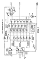
- FIG. 1 is a schematic diagram of a input ranging circuit 10 according to the present invention.
- the input ranging circuit 10 has three modes. Including d.c. volts mode, a.c. volts mode, and ohms mode, which are selected by a mode switch 12a-c.
- the mode switch 12a-c is a ganged switch having three positions corresponding to the three modes.
- An input terminal 11 is coupled to the mode switch 12c and receives an input voltage to be measured.
- the mode switch 12b-c selects between a DC PATH, an AC PATH, and an OHMS PATH according to the d.c. volts mode, a.c. volts mode, and ohms mode respectively.
- the input voltage received at the input terminal 11 is coupled through the DC PATH to one side of an input resistor 14 in a resistor array 16.
- the input resistor 14 is typically a very high resistance value in the range of 1 to 10 MegOhms in order to minimize the loading effects of the electronic instrument on the measurement.
- the other side of the input resistor 14 is coupled to a switch array 18.
- the switch array contains switches a-f coupled to a DIVIDER bus, switches g-1 coupled to a SOURCE bus and switches m-r coupled to a SENSE bus.
- Each of the switches a-r is independently controllable via control signals (not shown) preferably generated by a microprocessor or digital controller.
- Each of the switches a-r typically comprise field effect transistors (FET) or other low leakage electronic switches that are commercially available.
- the resistor array 16 is preferably implemented in a monolithic array in which the material comprising each resistor is deposited on a common substrate. Because the accuracy of the voltage scaling directly depends on the accuracy of the ratiometric tolerances of the resistors in the resistor array 16, the full advantage of the present invention may be realized from utilizing the relatively, tight ratiometric tolerances between each of the resistors that may be obtained in a monolithic array according to ratiometric scaling. It is desirable that the same resistor array 16 be used for all three modes in the input ranging circuit 10 in order to provide enhanced accuracy ranging for d.c. volts, a.c. volts, and resistance.
- the input resistor 14 is coupled to the DIVIDER bus via the switch b.
- the DIVIDER bus in turn is connected via one of the switches c-f to a selected divider resistor among the set of divider resistors 20-26 according to a selected divider ratio.
- Each of the divider resistors 20-26 is connected to ground in d.c. volts mode.
- the set of divider resistors 20-26 typically have values organized by decide values, such as 100 kiloOhms, 10 kiloOhms, and 1 kiloOhms. In order to provide division of the input voltage by decades; such as 10:1, 100:1, and 1000:1 according to a set of divider ratios.
- the ratiometric scaling of the set of divider resistors with the input resistor allows higher accuracy for the set of divider ratios.
- the output voltage DC OUT is developed at the SENSE bus which is selectively connected via one of the switches m-r to the junction of the input resistor and selected divider resistor formed by the DIVIDER bus.
- FIG. 2 provides a simplified schematic diagram of the input ranging circuit 10 configured for d.c. volts mode.
- the input voltage is connected via the input terminal 11 to the input resistor 14 and further to the DIVIDER bus to the selected one of the set of divider resistors 20-26 which are coupled to ground.
- the output voltage DC OUT is developed via the SENSE bus which is coupled to the junction of the input resistor 14 and the selected divider resistor formed by the DIVIDER bus, and thus equals the ratio of the divider resistor value to the input resistor value times the input voltage.
- the input signal is coupled to the input terminal 11 which is coupled via a capacitor 28 to the input resistor 14.
- the other side of the input resistor 14 is coupled via the switch b to the DIVIDER bus.
- the DIVIDER bus in turn is coupled via one of the switches c-f to a selected divider resistor among the set of divider resistors 20-26 according to a selected divider ratio.
- Each of the divider resistors 20-26 is in turn coupled to the junction of feedback resistors 30 and 32.
- the other end of the feedback resistor 30 is coupled to an output of an AC amplifier 34.
- the feedback resistor 32 is coupled to ground.
- An inverting input of the a.c. amplifier 34 is coupled via a switch s to the SENSE bus which is selectively, connected via one of the switches m-r to the junction of the input resistor 14 and the selected divider resistor formed by the DIVIDER bus.
- the output voltage AC OUT is developed at the output of the AC amplifier 34.
- the feedback resistors 30 and 32 set the gain of the AC amplifier 34 and allow a lower value of divider resistance to be used from the set of divider resistors 20-26 than for the divider resistance required for the same divider ratio in the d.c. volts mode.
- the junction of the feedback resistors 30 and 32 is an active node by virtue of the operation of the gain of the AC amplifier 34, thereby reducing the effects of parasitic capacitance (not shown) that appear in shunt across the input resistor 14 and each of the divider resistors 20-26. thereby increasing the useful bandwidth of the input ranging circuit 10 and eliminating the need for adjustments and trimming.
- the feedback resistor 30 has a value of 900 ohms and the feedback resistor 32 has a value of 100 ohms which provides for an amplifier gain of 10, thereby reducing the value of the resistance required for one of the divider resistors 20-26 by a decade and proportionately reducing the effects of the parasitic capacitance on the bandwidth.
- the AC amplifier 34 may be configured for unity gain, operating only as a buffer amplifier for selected divider ranges, by appropriate selection of switches s, t, u, and v, and still achieve some advantage in extended bandwidth.
- the switches s, t, u, and v are preferably part of the same integrated circuit device comprising the switch array 18.
- the switch array 18 is preferably constructed using a custom integrated circuit to save component count and manufacturing cost but may also constructed using commercially available integrated circuits having a number of switches that are coupled together externally.
- FIG. 3 provides a simplified schematic diagram of the input ranging circuit 10 configured for a.c. volts mode.
- the input voltage is coupled to the input 1 and further to the capacitor 28 and the input resistor 14.
- the other side of the input resistor 14 is coupled via the DIVIDER bus to the selected one of the set of divider resistors 20-26, which in turn are coupled to the junction of the feedback resistors 30 and 32.
- the inverting input of the AC amplifier 34 is coupled to the SENSE bus which is coupled to the junction of the input resistor 14 and the selected one of the set of divider resistors 20-26 formed by the DIVIDER bus.
- the output voltage AC OUT is developed at the output of the AC amplifier 34 according to the ratio of the divider resistor value to the input resistor value times the gain of the AC amplifier 34.
- the feedback resistors 30 and 32 are ratiometrically scaled with each other and with the set of divider resistors 20-26 in order to arrive at a more accuracte scale factor for the output voltage AC OUT.
- a resistor Rx (not shown) having an unknown resistance is coupled to the input terminal 11 which couples the resistor Rx via an OHMS PATH to a current source and an OHMS SENSE output.
- the resistor Rx is coupled to receive a programmable current I prog and the voltage drop across the resistor Rx is measured to determine the resistance based on I prog and the voltage drop.
- the resistor Rx preferably has separate source and sense Kelvin connections (not shown) for enhanced accuracy, as is known in the art for resistance measurements.
- a reference resistor 36 is coupled between the supply voltage +V and a noninverting input of an amplifier 38 and further coupled to a current source 40 which produces a reference current I ref to produce a reference voltage V ref .
- a selected one of the set of divider resistors 20-26 is coupled between +V and a transistor 42 via one of switches g-1 and the SOURCE bus.
- An inverting input of the amplifier 38 is coupled via a switch w to the SENSE bus and one of the switches m-r to the transistor 42.
- An output of the amplifier 38 is coupled to a control input of the transistor 42 to control the amount of current I prog flowing through the transistor 42.
- the reference resistor 36 is ratiometrically scaled with the set of divider resistors 20-26 to obtain improved accuracy of I prog .
- FIG. 4 is a simplified schematic diagram of the input ranging circuit 10 in the ohms mode.
- the reference resistor 36, amplifier 38, current source 40, divider resistors 20-26, and transistor 42 comprise a current source that produces a current I prog that is scaled according to the ratio of the reference resistor 14 to the selected one of the set of divider resistors 20-26 times the reference current I ref .
- I prog flows through the resistor Rx via the OHMS PATH to produce a voltage drop that is coupled to the OHMS SENSE output. I prog is thus selected to obtain a scaled voltage level at the OHMS SENSE output in a range that may be readily measured by the electronic instrument.
Landscapes
- Physics & Mathematics (AREA)
- General Physics & Mathematics (AREA)
- Measurement Of Current Or Voltage (AREA)
- Analogue/Digital Conversion (AREA)
Abstract
Description
Claims (9)
- An input ranging circuit, comprising:(a) an input terminal adapted for receiving an input voltage;(b) a mode switch coupled to said input terminal for selecting one of an a.c. volts mode and a d.c. volts mode;(c) a resistor array coupled to said mode switch, said resistor array comprising a plurality of ratiometrically scaled resistances;(d) an a.c. amplifier coupled to said plurality of ratiometrically scaled resistances to produce an a.c. output voltage according to a gain, said gain set according to said plurality of ratiometrically scaled resistances;(e) a switch array coupled to said plurality of ratiometrically scaled resistors and to said a.c. amplifier to obtain a selected scaling of said input signal wherein:(i) in said d.c. volts mode, a d.c. output voltage is scaled from said input voltage according to said ratiometrically scaled resistors, and(ii) in said a.c. volts mode, said a.c. output voltage is scaled from said input voltage according to said ratiometrically scaled resistors and said gain of said a.c. amplifier.
- An input ranging circuit according to claim 1, said mode switch further selecting an ohms mode.
- An input ranging circuit according to claim 2 further comprising a current source, said current source comprising an amplifier coupled to said reference resistor to produce a programmable current scaled according to said ratiometrically scaled resistors wherein in said ohms mode said programmable current is coupled across an unknown resistance at said input terminal.
- An input ranging circuit according to claim 2 wherein said mode switch further selects one of a d.c. path, an a.c. path, and an ohms path from said input terminal according to said d.c. volts mode, said a.c. volts mode, and said ohms mode.
- An input ranging circuit according to claim 1, said resistor array further comprising:(a) an input resistor coupled to said input terminal;(b) a plurality of divider resistors selectively coupled to said input resistor by said switch array; and(c) a plurality of feedback resistors selectively coupled to said a.c. amplifier by said switch array to determine said gain of said a.c. amplifier.
- An input ranging circuit according to claim 1, said switch array further comprising:(a) a divider bus, a source bus, and a sense bus; and(b) a plurality of switches coupled between each of said divider bus, said source bus, and said sense bus and said input resistor and said plurality of divider resistors.
- An input ranging circuit, comprising:(a) an input terminal adapted for receiving an input voltage;(b) a mode switch coupled to said input terminal for selecting one of an a.c. volts mode, a d.c. volts mode, and an ohms mode;(c) a resistor array coupled to said mode switch, said resistor array comprising an input resistor, a reference resistor, a plurality of divider resistors, and a plurality of feedback resistors, said input resistor coupled to said mode switch to receive said input voltage;(d) an a.c. amplifier coupled to said feedback resistors to produce an a.c. output voltage;(e) a current source comprising an amplifier coupled to said reference resistor and said plurality of divider resistors to produce a programmable current;(f) a switch array coupled to said input resistor, said plurality of divider resistors, and said a.c. amplifier, said switch array comprising a divider bus, a source bus, and a sense bus, and a plurality of switches coupled between each of said divider bus, said source bus, and said sense bus and said input resistor and said plurality of divider resistors wherein:(i) in said d.c. volts mode, a d.c. output voltage is developed from said sense bus coupled to a junction of said input resistor and a selected one of said plurality of divider resistors through said divider bus,(ii) in said a.c. volts mode, said a.c. output voltage is developed from said a.c. amplifier coupled to said junction of said input resistor and said selected one of said plurality of divider resistors through said divider bus and said sense bus, and,(iii) in said ohms mode, an ohms sense voltage is developed across an unknown resistor coupled to said input terminal responsive to said programmable current.
- An input ranging circuit according to said claim 7 wherein said mode switch further selects one of a d.c. path, an a.c. path, and an ohms path from said input terminal according to said d.c. volts mode, said a.c. volts mode, and said ohms mode.
- An input ranging circuit according to said claim 7 wherein said input resistor, said reference resistor, said plurality of divider resistors, and said plurality of feedback resistors are ratiometrically scaled.
Applications Claiming Priority (2)
| Application Number | Priority Date | Filing Date | Title |
|---|---|---|---|
| US08/936,482 US6094045A (en) | 1997-09-18 | 1997-09-18 | Input ranging circuit for an electronic instrument |
| US936482 | 1997-09-18 |
Publications (3)
| Publication Number | Publication Date |
|---|---|
| EP0903585A2 true EP0903585A2 (en) | 1999-03-24 |
| EP0903585A3 EP0903585A3 (en) | 2000-04-05 |
| EP0903585B1 EP0903585B1 (en) | 2002-12-11 |
Family
ID=25468707
Family Applications (1)
| Application Number | Title | Priority Date | Filing Date |
|---|---|---|---|
| EP98307331A Expired - Lifetime EP0903585B1 (en) | 1997-09-18 | 1998-09-10 | Input ranging circuit for an electronic instrument |
Country Status (3)
| Country | Link |
|---|---|
| US (1) | US6094045A (en) |
| EP (1) | EP0903585B1 (en) |
| DE (1) | DE69810046T2 (en) |
Cited By (8)
| Publication number | Priority date | Publication date | Assignee | Title |
|---|---|---|---|---|
| EP1158302A3 (en) * | 2000-05-23 | 2003-10-22 | Tektronix, Inc. | Method and apparatus for probing a conductor of an array of closely-spaced conductors |
| CN101354410B (en) * | 2008-08-28 | 2010-12-08 | 骆晓英 | DC potential difference meter using slide wire disc |
| CN101813721B (en) * | 2008-08-28 | 2011-08-10 | 骆晓英 | Pressure measuring instrument |
| CN101813722B (en) * | 2008-08-28 | 2011-09-07 | 骆晓英 | Three-range potential difference meter |
| CN101788590B (en) * | 2008-08-28 | 2011-10-05 | 骆晓英 | Voltage measuring device |
| CN101788587B (en) * | 2008-08-28 | 2011-10-05 | 骆晓英 | Voltage measuring instrument |
| CN101776704B (en) * | 2009-12-30 | 2013-02-27 | 富阳精密仪器厂 | Voltage-measuring device with four measuring panels |
| CN119555979A (en) * | 2025-02-06 | 2025-03-04 | 青岛锐捷智能仪器有限公司 | A multi-level excitation generation system and method for lithium battery impedance measurement |
Families Citing this family (15)
| Publication number | Priority date | Publication date | Assignee | Title |
|---|---|---|---|---|
| US7177707B2 (en) * | 1998-10-09 | 2007-02-13 | Peter Ar-Fu Lam | Variable specification functional blocks integrated circuit system suitable for detecting resistor identifications |
| US6323633B1 (en) * | 1999-10-12 | 2001-11-27 | The United States Of America As Represented By The Secretary Of The Army | Device and method for detection and/or inspection of conductive particles using high-voltage field |
| US6794859B2 (en) * | 2002-11-20 | 2004-09-21 | Sang J. Choi | Automatic multimeter |
| US20050017760A1 (en) * | 2003-07-22 | 2005-01-27 | International Rectifier Corporation | Current sense shunt resistor circuit |
| US7034517B2 (en) * | 2004-03-15 | 2006-04-25 | Fluke Corporation | Multimeter with filtered measurement mode |
| CN101055279B (en) * | 2007-05-29 | 2010-05-26 | 方李 | Portable potentiometer |
| CN101059536B (en) * | 2007-05-29 | 2010-05-26 | 方李 | Two-range potentiometer adopting transposition branch |
| CN101063694B (en) * | 2007-05-29 | 2010-06-02 | 张春雷 | Voltage measurement instrument |
| US8193945B2 (en) * | 2008-01-11 | 2012-06-05 | Lear Corporation | System and method for remote activation using a transmitter switch array |
| TWI361281B (en) * | 2008-04-17 | 2012-04-01 | Cyrustek Co | A measurement unit including an auto switch low-pass filter |
| US8346496B1 (en) * | 2009-08-27 | 2013-01-01 | Wildcat Disocovery Technologies, Inc | Apparatus and method for multi-channel materials assaying |
| CN101769951B (en) * | 2009-12-30 | 2012-10-24 | 富阳精密仪器厂 | Two-measuring-range potential difference meter with four metering panels |
| JP6495110B2 (en) * | 2015-06-15 | 2019-04-03 | 日置電機株式会社 | Resistance measuring device |
| DE202018103787U1 (en) | 2018-07-02 | 2018-09-24 | Johnson Electric Germany GmbH & Co. KG | Electric microswitch |
| US11057002B2 (en) | 2019-06-18 | 2021-07-06 | Analog Devices International Unlimited Company | Amplifier configurable into multiple modes |
Family Cites Families (5)
| Publication number | Priority date | Publication date | Assignee | Title |
|---|---|---|---|---|
| DE3360928D1 (en) * | 1982-07-02 | 1985-11-07 | Thorn Emi Instr | Improvements in or relating to multimeters |
| US5332963A (en) * | 1990-02-15 | 1994-07-26 | John Fluke Mfg. Co., Inc. | High input impedance buffer with low feedback resistance |
| DE4139855A1 (en) * | 1991-12-03 | 1993-06-09 | Kabushiki Kaisha Sanwa Keiki Seisakusho, Akishima, Tokio/Tokyo, Jp | Analogue multimeter for measuring voltage, current and resistance - has autoranging attenuator circuit and indicates selected measurement range |
| US5373410A (en) * | 1992-03-27 | 1994-12-13 | Tandy Corporation | Single string resistive divider network for a digital multimeter |
| US5463315A (en) * | 1993-06-15 | 1995-10-31 | Hewlett-Packard Company | Spike suppression for a tester circuit for integrated circuits |
-
1997
- 1997-09-18 US US08/936,482 patent/US6094045A/en not_active Expired - Lifetime
-
1998
- 1998-09-10 DE DE69810046T patent/DE69810046T2/en not_active Expired - Lifetime
- 1998-09-10 EP EP98307331A patent/EP0903585B1/en not_active Expired - Lifetime
Cited By (8)
| Publication number | Priority date | Publication date | Assignee | Title |
|---|---|---|---|---|
| EP1158302A3 (en) * | 2000-05-23 | 2003-10-22 | Tektronix, Inc. | Method and apparatus for probing a conductor of an array of closely-spaced conductors |
| CN101354410B (en) * | 2008-08-28 | 2010-12-08 | 骆晓英 | DC potential difference meter using slide wire disc |
| CN101813721B (en) * | 2008-08-28 | 2011-08-10 | 骆晓英 | Pressure measuring instrument |
| CN101813722B (en) * | 2008-08-28 | 2011-09-07 | 骆晓英 | Three-range potential difference meter |
| CN101788590B (en) * | 2008-08-28 | 2011-10-05 | 骆晓英 | Voltage measuring device |
| CN101788587B (en) * | 2008-08-28 | 2011-10-05 | 骆晓英 | Voltage measuring instrument |
| CN101776704B (en) * | 2009-12-30 | 2013-02-27 | 富阳精密仪器厂 | Voltage-measuring device with four measuring panels |
| CN119555979A (en) * | 2025-02-06 | 2025-03-04 | 青岛锐捷智能仪器有限公司 | A multi-level excitation generation system and method for lithium battery impedance measurement |
Also Published As
| Publication number | Publication date |
|---|---|
| DE69810046D1 (en) | 2003-01-23 |
| DE69810046T2 (en) | 2003-07-17 |
| US6094045A (en) | 2000-07-25 |
| EP0903585A3 (en) | 2000-04-05 |
| EP0903585B1 (en) | 2002-12-11 |
Similar Documents
| Publication | Publication Date | Title |
|---|---|---|
| US6094045A (en) | Input ranging circuit for an electronic instrument | |
| US6307363B1 (en) | Ultrahigh-frequency high-impedance passive voltage probe | |
| US4857827A (en) | Electronic load for testing transformers | |
| US5621310A (en) | High frequency calibration circuit | |
| US5801525A (en) | Frequency discriminating power sensor | |
| US4897599A (en) | Signal processing device with a level adapter circuit | |
| US4833400A (en) | High frequency multi-range attenuator having a high input impedance | |
| US4206416A (en) | Wideband instrumentation amplifier with high common mode rejection | |
| US6836107B2 (en) | Constant input impedance AC coupling circuit for a current probe system | |
| EP0088561B1 (en) | Capacitor monitoring circuit | |
| JPH04212067A (en) | Dual-path wide-band high-precision data collecting system | |
| US5424677A (en) | Common mode error correction for differential amplifiers | |
| EP0035403A1 (en) | Voltage measuring instrument and preamplifier therefor | |
| EP0544396A1 (en) | Instruments for measuring the frequency and power of a microwave signal | |
| CA2129556C (en) | Impedance synthesizer | |
| CN113691236A (en) | Temperature compensation wideband signal attenuation circuit and control method thereof | |
| JP4216528B2 (en) | Calibration equipment for high-frequency signal measurement equipment | |
| EP0135214A1 (en) | Apparatus for measuring a temperature | |
| US5332963A (en) | High input impedance buffer with low feedback resistance | |
| Tarach et al. | High-accuracy N-port impedance measurement by means of modular digital AC compensators | |
| US3443215A (en) | Impedance measuring bridge with voltage divider providing constant source impedance to bridge | |
| KR101851967B1 (en) | Capacitor-registor bank apparatus for evaluating capacitance bridge | |
| US4599574A (en) | Selectable gain instrumentation amplifier | |
| US6977494B2 (en) | Switchable impedance circuit for current sensing an electricity meter | |
| US20060192571A1 (en) | Source measure circuit |
Legal Events
| Date | Code | Title | Description |
|---|---|---|---|
| PUAI | Public reference made under article 153(3) epc to a published international application that has entered the european phase |
Free format text: ORIGINAL CODE: 0009012 |
|
| AK | Designated contracting states |
Kind code of ref document: A2 Designated state(s): DE FR GB |
|
| AX | Request for extension of the european patent |
Free format text: AL;LT;LV;MK;RO;SI |
|
| PUAL | Search report despatched |
Free format text: ORIGINAL CODE: 0009013 |
|
| AK | Designated contracting states |
Kind code of ref document: A3 Designated state(s): AT BE CH CY DE DK ES FI FR GB GR IE IT LI LU MC NL PT SE |
|
| AX | Request for extension of the european patent |
Free format text: AL;LT;LV;MK;RO;SI |
|
| 17P | Request for examination filed |
Effective date: 20000517 |
|
| 17Q | First examination report despatched |
Effective date: 20000822 |
|
| AKX | Designation fees paid |
Free format text: DE FR GB |
|
| GRAG | Despatch of communication of intention to grant |
Free format text: ORIGINAL CODE: EPIDOS AGRA |
|
| GRAG | Despatch of communication of intention to grant |
Free format text: ORIGINAL CODE: EPIDOS AGRA |
|
| GRAH | Despatch of communication of intention to grant a patent |
Free format text: ORIGINAL CODE: EPIDOS IGRA |
|
| GRAH | Despatch of communication of intention to grant a patent |
Free format text: ORIGINAL CODE: EPIDOS IGRA |
|
| GRAA | (expected) grant |
Free format text: ORIGINAL CODE: 0009210 |
|
| AK | Designated contracting states |
Kind code of ref document: B1 Designated state(s): DE FR GB |
|
| REG | Reference to a national code |
Ref country code: GB Ref legal event code: FG4D |
|
| REF | Corresponds to: |
Ref document number: 69810046 Country of ref document: DE Date of ref document: 20030123 |
|
| ET | Fr: translation filed | ||
| PLBE | No opposition filed within time limit |
Free format text: ORIGINAL CODE: 0009261 |
|
| STAA | Information on the status of an ep patent application or granted ep patent |
Free format text: STATUS: NO OPPOSITION FILED WITHIN TIME LIMIT |
|
| 26N | No opposition filed |
Effective date: 20030912 |
|
| REG | Reference to a national code |
Ref country code: FR Ref legal event code: PLFP Year of fee payment: 19 |
|
| REG | Reference to a national code |
Ref country code: FR Ref legal event code: PLFP Year of fee payment: 20 |
|
| PGFP | Annual fee paid to national office [announced via postgrant information from national office to epo] |
Ref country code: FR Payment date: 20170925 Year of fee payment: 20 Ref country code: GB Payment date: 20170927 Year of fee payment: 20 |
|
| PGFP | Annual fee paid to national office [announced via postgrant information from national office to epo] |
Ref country code: DE Payment date: 20170927 Year of fee payment: 20 |
|
| REG | Reference to a national code |
Ref country code: DE Ref legal event code: R071 Ref document number: 69810046 Country of ref document: DE |
|
| REG | Reference to a national code |
Ref country code: GB Ref legal event code: PE20 Expiry date: 20180909 |
|
| PG25 | Lapsed in a contracting state [announced via postgrant information from national office to epo] |
Ref country code: GB Free format text: LAPSE BECAUSE OF EXPIRATION OF PROTECTION Effective date: 20180909 |