EP0903568A2 - Method for manufacturing a pressure measure device equipped with a resonating element - Google Patents
Method for manufacturing a pressure measure device equipped with a resonating element Download PDFInfo
- Publication number
- EP0903568A2 EP0903568A2 EP98203175A EP98203175A EP0903568A2 EP 0903568 A2 EP0903568 A2 EP 0903568A2 EP 98203175 A EP98203175 A EP 98203175A EP 98203175 A EP98203175 A EP 98203175A EP 0903568 A2 EP0903568 A2 EP 0903568A2
- Authority
- EP
- European Patent Office
- Prior art keywords
- layer
- top layer
- protective
- fact
- protective material
- Prior art date
- Legal status (The legal status is an assumption and is not a legal conclusion. Google has not performed a legal analysis and makes no representation as to the accuracy of the status listed.)
- Withdrawn
Links
Images


Classifications
-
- G—PHYSICS
- G01—MEASURING; TESTING
- G01L—MEASURING FORCE, STRESS, TORQUE, WORK, MECHANICAL POWER, MECHANICAL EFFICIENCY, OR FLUID PRESSURE
- G01L9/00—Measuring steady of quasi-steady pressure of fluid or fluent solid material by electric or magnetic pressure-sensitive elements; Transmitting or indicating the displacement of mechanical pressure-sensitive elements, used to measure the steady or quasi-steady pressure of a fluid or fluent solid material, by electric or magnetic means
- G01L9/0001—Transmitting or indicating the displacement of elastically deformable gauges by electric, electro-mechanical, magnetic or electro-magnetic means
- G01L9/0008—Transmitting or indicating the displacement of elastically deformable gauges by electric, electro-mechanical, magnetic or electro-magnetic means using vibrations
- G01L9/0019—Transmitting or indicating the displacement of elastically deformable gauges by electric, electro-mechanical, magnetic or electro-magnetic means using vibrations of a semiconductive element
Definitions
- the present invention relates to a method for manufacturing a pressure-measuring device equipped with a resonating element.
- the invention relates to a method for manufacturing a pressure-measuring device for measuring absolute, relative or differential pressure.
- the pressure-measuring device that can be manufactured using the procedure as in the invention is, for example, of the type described in Italian patent application No. MI96A002268, filed in the name of the same applicant as the present application, the disclosure of which is incorporated herein for reference.
- pressure-measuring devices can be prepared by suitably machining wafers of semiconductor-based materials.
- silicon micromachining are widely used for manufacturing sensors using silicon as the base material.
- micromachining technologies are very similar to those used for the production of microelectronic circuits. With a single process, it is possible to machine a considerable number of devices that are identical to one another with significant advantages in terms of production costs.
- Micromachining generally comprises technologies such as thin layer deposition (a few microns thick) of semiconductor materials and their derivatives or metal materials, extremely precise photolithographic techniques (resolutions of less than one micron), selective removal of semiconductor material through the action of suitable chemical agents, bonding techniques on separate layers.
- silicon micromachining technologies can be divided into two main categories known as “bulk micromachining” technologies and “surface micromachining” technologies.
- the former refers to the possibility of obtaining monocrystalline structures by machining both sides of a wafer of semiconductor material, whereas the latter refers to machining performed on one side of the wafer only.
- “Surface micromachining” technologies are highly innovative compared to the former and make it possible to manufacture smaller microstructures (one order of magnitude smaller). They also offer the considerable advantage of easier machining and greater potential for integrating the structures produced with microelectronic circuits made in the same chip of semiconductor material.
- the main task of the present invention is therefore to provide a method for manufacturing a pressure-measuring device, based on a resonating element, that is capable to give high performances.
- one object of the present invention is to provide a method for manufacturing a pressure-measuring device that makes it possible to integrate the resonating element of the device with the diaphragm to which the pressure is applied.
- Another object of the present invention is to provide a method for manufacturing a pressure-measuring device, that enables the production in batches of the device.
- Another object of the present invention is to provide a method for manufacturing a pressure-measuring device by which it is possible to produce three-dimensional structures using either technologies for machining on both sides of the wafer or technologies for machining on a single side.
- a further object of the present invention is to provide a method for manufacturing a pressure-measuring device in which the resonating element operates under a high vacuum and is protected from overrange pressure pulses.
- Yet another object of the present invention is to provide a method for manufacturing a pressure-measuring device in which the machining for making the resonating element is performed on one side of the wafer only.
- a further though not the last object of the present invention is to provide a pressure-measuring device that is highly reliable and relatively easy to manufacture at competitive costs.
- a method for manufacturing a pressure-measuring device comprising a diaphragm of semiconductor material having a resonating element fixed thereto, said diaphragm being exposed to the pressure of a process fluid.
- the method of the present invention is characterised by the fact that it comprises the following phases:
- the present invention is a combination of the above described silicon micromachining technologies. This solution is particularly advantageous compared to the prior art, because it allows to perform the most critical machining steps working on a single plane, even when a three-dimensional structure is manufactured.
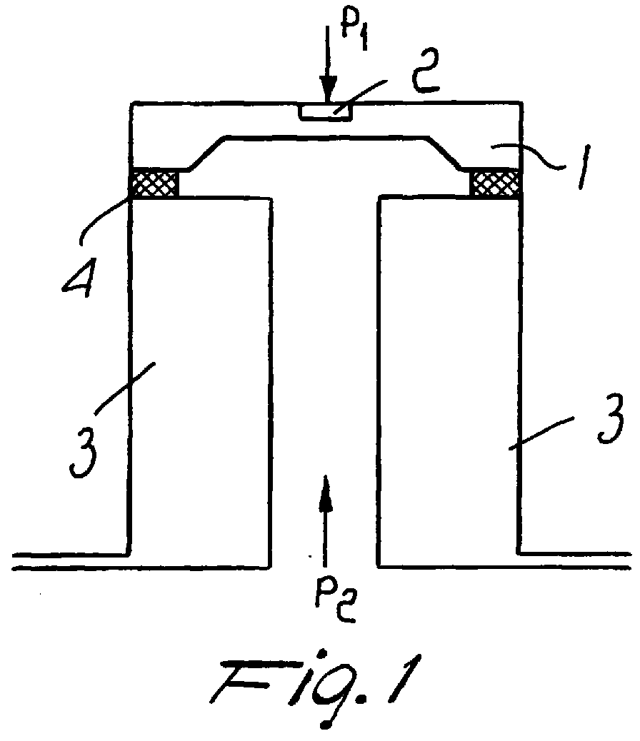
- Figure 1 shows the overall structure of the device to be manufactured using the procedure as in the invention.
- the diaphragm 1, to which the resonating element 2 is fixed in such a way as to form an integral part of the former, is mounted on a suitable support 3 using a substrate 4 of insulating material.
- the diaphragm is in this way exposed to the action of two pressures P1 and P2, the the difference of which has to be measured.
- Figure 2 shows a preferred embodiment of the device manufactured using the method as in the invention.
- the diaphragm 1 is bonded to a layer of semiconductor material 5 in order to protect the resonating element 8 and advantageously allowing it to vibrate in a cavity where a high vacuum is kept.
- Bonding between the diaphragm 1 and the layer 5 generally is carried out interposing a layer of semiconductor material (not shown in figure 2).
- the diaphragm 1 also features a protrusion 7 on the opposite side designed to abut against the support layer of semiconductor material 6 bonded to the diaphragm 1 using a layer of insulating material.
- the support layer 6 is bonded to a further support 3 using a layer of insulating material 4.
- Figure 3 shows a DETF (Double Ended Tuning Fork) resonating structure, seen in plan view, together with excitation and detection elements as in a preferred embodiment.
- DETF Double Ended Tuning Fork
- the resonating element 8 features two parallel arms 9 and 10 that vibrate laterally.
- the resonating element is fixed to the diaphragm 1 using connection portions 11 and 12.
- Said portions 11 e 12 (referred to as detection element) are electrically insulated from the rest of the system using a separating cavity 13. Their function is to detect the frequency signal proportional to the pressure applied to the diaphragm at the ends of the resonating element 8.
- excitation element two other portions of diaphragm 14 and 15 (referred to as excitation element) are made in such a way as to enable the resonating element 8 to be excited.
- the cavity 13 also extends under the resonating element 8 to enable it to vibrate freely.
- Elements 11 and 12 are partially covered by layers 16 and 17 of suitably-shaped metal material to facilitate the transmission of the detection signal to the outside environment.
- elements 14 and 15 of the diaphragm are covered by metal layers 18 and 19 that are used to carry the excitation signal to the sensor.
- Figure 4 shows a plan view of the diaphragm from which the resonating structure and excitation and detection elements are obtained using the procedure as in the present invention.
- Figure 5 shows a view in perspective of the zone of the diaphragm 1 close to the resonating element.
- Figure 6 shows a section view along line VI-VI in Figure 3.
- the method as in the invention can be divided into three main parts:
- the bonding of a protective layer 5 seals the cavity allowing the resonating element 8 to vibrate in high vacuum.
- a multilayer structure of semiconductor material consisting of three layers of semiconductor materials 22, 23 and 24 in (respectively referred as top layer, intermediate layer and bottom layer) can be advantageously used as starting material for the machining process.
- Three-layer semiconductor wafers already available on the market SOI wafers for example can be conveniently used, thus assuring the quality and repeatability of the structure on which machining is commenced.
- phase i) comprises the following steps:
- the machining phase i) is carried out on the surface of the wafer indicated as "A" in Figure 7.
- the step a) comprises:
- the removal of layer 26 can be performed immediately before removing the layer 25.
- step b) comprises:
- step b) can comprises the following steps:
- step c) comprises:
- phase i) The steps comprised in phase i) can be carried out advantageously in different orders such as:
- Phase ii) relates to the machining of the layers 6 in figure 2, which features an opening for making the pressure port 21. Silicon wafers available on the market can be used. Techniques similar to those used in phase iv) described herebelow can be adopted.
- layer 6 can feature a greater number of pressure ports 21 to enable easier flow of the process oil in the zone beneath the diaphragm 1.
- phase iv) comprises:
- This machining of the protective structure 7 can advantageously be performed independently from phase i).
- Phases iii), v) and vi) include bonding processes between different layers, that can be carried out using the same techniques.
- phase v) can be performed to enable the resonator 8 to be housed in a cavity that is kept at high vacuum.
- the machining is carried out on the surface "A" of the top layer 22.
- phase v) can be divided into the following steps:
- Phase iii) can be performed using the technologies described above.
- phase vi) can be implemented using the technologies described above.
- the method according to the invention fully achieves its set objectives in that the method as in the invention makes it possible to manufacture a resonating element on a silicon diaphragm using silicon machining technologies that enable to perform the most critical machining on one side of the wafer only, integrating the excitation and detection elements and the resonating element with the structure itself; the less critical processes are carried out on the other side of the wafer.
- the resonating element can vibrate in a high vacuum and moreover can be protected against considerable pressure pulses during operation.
- SOI wafer allows to create monocrystalline silicon structures and therefore improve the mechanical performance of the resonator compared to structures that use other materials such as polysilicon and quartz.
- the phase for doping the chip is carried out on the whole chip except for the resonating element.
- This choice has three advantages: in the first place it is avoided the occurrence of gradients in the doping profile, in addition it is avoided the occurrence of leakage current due to many electrons on the Si/covering SiO2 interface and, finally, simpler masks can be used.
- phase i), ii), iii), iv), v) and vi) can also be performed following a different order from what set out above, although it has been found that the above is the most logical process phase sequence for obtaining the pressure measuring device object of the invention.
- the dimensions and materials used can be of any kind to suit requirements and the state of technology providing they are compatible with the specific use.
Landscapes
- Physics & Mathematics (AREA)
- General Physics & Mathematics (AREA)
- Measuring Fluid Pressure (AREA)
Abstract
Description
- depositing a layer of protective material 25 (SiO2 for example) on the surface
referred as "A" of the
top layer 22 of the three-layer semiconductor material (Figure 8a); - depositing of a layer of photosensitive material 26 (resist for example) (Figure 8b);
- removing portions 27 in the layer of resist 26 (Figure 8c) using a suitable
photolithographic process. The light radiation used in the photolithographic
process makes the portions 27 sensitive to chemical agents, thus allowing their
removal. The
layer 26 can be used as a mask defining the profile of the resonating element, the excitation element and the detection element; - removing the
unmasked portions 28 in thelayer 25; this removal can be performed using wet etching. Thelayer 25 can be used as a mask for thetop layer 22; - removing the layer 26 (figure 8d);
- removing the
unmasked portions 29 in thelayer 22 until reaching theintermediate layer 23 of the three-layer semiconductor material used (see figure 8e). A dry removal process can be used. Using a dry process allows to create highly anisotropic structures. The structures of the resonatingelement 8, the excitation and the detection elements is thus defined on thetop layer 22; - masking with a layer of protective material 30 (such as resist, for example) the
cavities in the
top layer 22; - removing the layer 25 (for example by chemical etching). This cannot remove
the
intermediate layer 23 thanks to the protective action of thelayer 30. (See figure 8g).
- covering surface "A" of the
top layer 22 with a layer ofprotective material 31; - selectively removing portions of
layer 31 creating a mask defining thereon the path of theelectrical connections - selectively removing portions of the top layer 22 (for example with partially
anisotropic etching). This creates
cavities - removing layers of
protective material 30 and 31 (see Figure 9b); - masking with a layer of protective material 34 (such as resist, for example) the portion of the top layer where the resonator has to be positioned (see figure 10);
- selectively doping the unmasked portions of the
top layer 22. Known ion implantation techniques can advantageously be used for the doping; - selectively removing the protective layer 34 from the surface "A" of the top layer 22 (see figure 11a);
- covering the
top layer 22 with a layer ofmetallic material 36. Sputtering or metal evaporation techniques can be used (see figure 11b). More layers of different metallic materials can be deposited; - masking the portions of
layer 36 matching withseatings - selectively removing the unmasked portions of
layer 36; - removing all the protective material from the top layer 22 (Figure 11c).
- covering the
top layer 22 with a layer of protective material; - selectively removing portions of said layer of protective material using photolithographic techniques to create a mask defining thereon the path of said electrical connections;
- selectively removing the unmasked portions of the top layer creating cavities for the seatings of said electrical connections;
- removing of said protective material;
- masking the portion of the top layer, where said resonator has to positioned, using a layer of protective material;
- selectively doping the unmasked portions of the top layer;
- masking with a layer of protective material the portion of the
top layer 22 not occupied by the seatings of said electrical connections; - depositing metallic material into said seatings; and
- removing said protective material;
- cleaning the
top layer 22; - covering
layer 22 with alayer 37 of protective material creating a mask with openings matching the area where the resonatingelement 8 is located (see figure 12a); - selectively removing the
intermediate layer 23. The removal is limited to the portion of material below the resonatingelement 8. A cavity allowing free vibration of the resonating element is created; - removing the protective layer 37 (see figure 12b);
- rinsing the three layer semiconductor material using solutions based for example on water, alchool or hydrocarbons.
- depositing a layer of protective material on the bottom layer 24 (see figure 7) said three-layer semiconductor material;
- selectively removing said protective material to create a mask defining the contour of said protection structure 7 (see figure 2);
- selectively removing the unmasked portion of the bottom layer of said three-layer
semiconductor material. Chemical etching can be performed because it is
anisotropic and exploits the different sensitivities of the various different
crystalline planes of the
layer 24 to the chemical agent; - removing said protective material.
- depositing a layer 38 (see figure 13) of insulating material on the surface "A" of
the
top layer 22. The deposition is performed on the entire surface of side "A" with the exception of the area of the resonatingelement 8. This can be achieved using masking techniques similar to those previously described. The layer of insulatingmaterial 38 can either be silicon dioxide or vitreous material and can be deposited using the techniques currently available, such as, for example, Plasma Enhanced Chemical Vapour Deposition, Low Temperature Oxidation, Low Pressure Chemical Vapour Deposition, Glass Sputtering, etc. - lapping
layer 38. This can advantageously be performed before the bonding process to increase the layer's planarity; - bonding layers 1 and 5 in figure 2. It is possible to use advantageously thermal anodic processes and catalysing solutions such as, for example, sodium silicate. Alternatively other thermal bonding processes can be used.
Claims (19)
- Method for manufacturing a pressure-measuring device comprising a diaphragm of semiconductor material having a resonating element fixed thereto, said diaphragm being exposed to the pressure of a process fluid, characterised by the fact that it comprises the following phases, whatever the order:i) machining a multilayer semiconductor material to obtain a diaphragm having on the upper side a resonating element, an excitation element and a detection element for measuring the pressure applied to said diaphragm;ii) machining a semiconductor material having one or more layers to obtain a support having a pressure port for the flow of the process fluid;iii) making a bond between the lower side of said diaphragm and the upper side of said support.
- Method as in claim 1 further comprising the following phase:iv) machining the lower part of the diaphragm to obtain a protective structure against overrange pressure pulses.
- Method as in one or more of the previous claims characterized by the fact that the multilayer semiconductor material used in phase i) is a three-layer semiconductor material having a top layer, an intermediate layer and a bottom layer.
- Method as in claim 3, characterized by the fact that the resonating element, the excitation element and related connections to the pad contacts and the detection elements and related connections to the pad contacts are created on the top layer of the three-layer semiconductor material.
- Method as in claim 3, characterized by the fact that the bottom layer is machined to obtain a protective structure against overrange pressure pulses.
- Method as in claim 4, characterized by the fact that the phase i) comprises the following steps:a) machining the top layer to selectively remove portions of said top layer and define thereon the structures of the resonating element, the excitation element and the detection element;b) creating metallized portions on said top layer in order to provide electrical connections to said excitation element and detection element; andc) selectively removing portions of the intermediate layer to create a cavity in said intermediate layer allowing free vibration of the resonating element.
- Method as in claim 6, characterised by the fact that said step a) comprises:depositing a layer of protective material on the surface of top layer;depositing a layer of photosensitive material over said layer of protective material;selectively remove portions of said photosensitive material using photolithografic techniques to create a mask defining the profile of the resonating element, excitation element and the detection element;selectively remove the unmasked portions of said protective layer.removing said mask of photosensitive material;removing portions of said top layer not masked by said protective layer creating openings reaching said intermediate layer;masking with a layer of protective material the portion of the top layer where the resonator has to be positioned; andremoving said layer of protective material on the surface of the top layer.
- Method as in claim 7, characterized by the fact that the removal of said mask of photosensitive material is carried out after making the openings in said top layer.
- Method as in claim 6, characterised by the fact that said step b) comprises:covering the top layer with a layer of protective material;selectively removing portions of said layer of protective material using photolithographic techniques to create a mask defining thereon the path of said electrical connections;selectively removing the unmasked portions of the top layer creating cavities for the seatings of said electrical connections;removing of said protective material;masking the portion of the top layer, where said resonator has to positioned, using a layer of protective material;selectively doping the unmasked portions of the top layer;removing said protective layer from the surface of the top layer;covering the top layer with one or more layers of metallic material;masking the portion of said layer of metallic material matching the seatings of said electrical connections;removing the unmasked portions of said layer of metallic material; andremoving the protective material.
- Method as in claim 6, characterised by the fact that said step b) comprises:covering the top layer with a layer of protective material;selectively removing portions of said layer of protective material using photolithographic techniques to create a mask defining thereon the path of said electrical connections;selectively removing the unmasked portions of the top layer creating cavities for the seatings of said electrical connections;removing said protective material;masking the portion of the top layer, where said resonator has to positioned, using a layer of protective material;selectively doping the unmasked portions of the top layer;masking with a layer of protective material the portion of the top layer not occupied by the seatings of said electrical connections;depositing metallic material into said seatings; andremoving said protective material;
- Method as in claim 6, characterised by the fact that said step c) comprises:cleaning the top layer of the three-layer material;covering the top layer with a layer of protective material creating a mask with openings matching the area where the resonating element is positioned;selectively removing the intermediate layer of said three-layer semiconductor material creating a cavity in said intermediate layer allowing free vibration of the resonating element.removing said protective material; andrinsing said three-layer semiconductor material using cleaning solutions.
- Method as in one or more of the claims from 6 to 11, characterised by the fact that the phase i) comprises the steps described in claim 6 with the following order:step a), step b) and step c).
- Method as in one or more of the claims from 6 to 11, characterized by the fact that said phase i) comprises the steps described in claim 6 in the following order:step a), step c) and step b).
- Method as in claim 5, characterized by the fact that the machining of the bottom layer comprises:depositing a layer of protective material on the bottom layer of said three-layer semiconductor material;selectively removing said protective material to create a mask defining the contour of said protection structure; andselectively removing the unmasked portion of the bottom layer of said three-layer semiconductor material; andremoving said protective material.
- Method as in one or more of the previous claims, further comprising the following phase:v) making a bond on the lower side of said support and a further support.
- Method as in one or more of the previous claims, further comprising the following phase:vi) making a bond between the upper side of said diaphragm and a protective layer.
- Method as in claim 16 characterized by the fact that said phase vi) comprises:depositing an insulating layer on the portion of the top layer not comprising the resonating element;lapping said insulating layer ;bonding said insulating layer and said protective layer.
- Method as claims 16 or 17 characterized by the fact that said bond of a protective layer seals the cavity in the intermediate layer of said three-layer semiconductor material allowing free vibration of the resonating element in high vacuum.
- Pressure measuring device obtained according to a method as in one or more of the previous claims.
Applications Claiming Priority (3)
| Application Number | Priority Date | Filing Date | Title |
|---|---|---|---|
| ITMI972121 | 1997-09-18 | ||
| IT97MI002121A IT1295031B1 (en) | 1997-09-18 | 1997-09-18 | PROCEDURE FOR MANUFACTURING A PRESSURE MEASURING DEVICE EQUIPPED WITH A RESONANT ELEMENT |
| US09/186,647 US6207470B1 (en) | 1997-09-18 | 1998-11-06 | Method for manufacturing a pressure-measuring device equipped with a resonating element |
Publications (2)
| Publication Number | Publication Date |
|---|---|
| EP0903568A2 true EP0903568A2 (en) | 1999-03-24 |
| EP0903568A3 EP0903568A3 (en) | 1999-12-01 |
Family
ID=26331540
Family Applications (1)
| Application Number | Title | Priority Date | Filing Date |
|---|---|---|---|
| EP98203175A Withdrawn EP0903568A3 (en) | 1997-09-18 | 1998-09-18 | Method for manufacturing a pressure measure device equipped with a resonating element |
Country Status (3)
| Country | Link |
|---|---|
| US (1) | US6207470B1 (en) |
| EP (1) | EP0903568A3 (en) |
| IT (1) | IT1295031B1 (en) |
Cited By (1)
| Publication number | Priority date | Publication date | Assignee | Title |
|---|---|---|---|---|
| EP2986024A1 (en) * | 2014-08-13 | 2016-02-17 | Samsung Electronics Co., Ltd | Audio sensing device and method of acquiring frequency information |
Families Citing this family (7)
| Publication number | Priority date | Publication date | Assignee | Title |
|---|---|---|---|---|
| US6498086B1 (en) * | 2001-07-26 | 2002-12-24 | Intel Corporation | Use of membrane properties to reduce residual stress in an interlayer region |
| DE102004006197B4 (en) * | 2003-07-04 | 2013-10-17 | Robert Bosch Gmbh | Method for producing a micromechanical pressure sensor |
| JP2006228776A (en) * | 2005-02-15 | 2006-08-31 | Advantest Corp | Charged particle beam exposure apparatus and charged particle beam exposure method |
| US7042230B1 (en) | 2005-02-28 | 2006-05-09 | Alain Izadnegahdar | Multi-parameter sensing system |
| US7069790B1 (en) * | 2005-05-17 | 2006-07-04 | Honeywell International Inc. | Systems and methods for measuring relative thermal expansion coefficient of low thermal coefficient of expansion materials |
| DE102009002990A1 (en) * | 2009-05-11 | 2010-11-18 | Robert Bosch Gmbh | High pressure sensor |
| JP6465097B2 (en) * | 2016-11-21 | 2019-02-06 | 横河電機株式会社 | Vibrating transducer |
Family Cites Families (11)
| Publication number | Priority date | Publication date | Assignee | Title |
|---|---|---|---|---|
| EP0456029B1 (en) * | 1990-05-10 | 1994-12-14 | Yokogawa Electric Corporation | Vibrating type pressure measuring device |
| DE4333099A1 (en) * | 1993-09-29 | 1995-03-30 | Bosch Gmbh Robert | Force sensor and process for producing a force sensor |
| JP3551527B2 (en) * | 1994-04-27 | 2004-08-11 | 株式会社デンソー | Method for manufacturing semiconductor strain-sensitive sensor |
| US5646072A (en) * | 1995-04-03 | 1997-07-08 | Motorola, Inc. | Electronic sensor assembly having metal interconnections isolated from adverse media |
| AU4801297A (en) * | 1996-10-07 | 1998-05-05 | Lucas Novasensor | Silicon at least 5 micron high acute cavity with channel by oxidizing fusion bonding and stop etching |
| IT1287123B1 (en) * | 1996-10-31 | 1998-08-04 | Abb Kent Taylor Spa | DEVICE FOR MEASURING A PRESSURE |
| US6069392A (en) * | 1997-04-11 | 2000-05-30 | California Institute Of Technology | Microbellows actuator |
| US5994161A (en) * | 1997-09-03 | 1999-11-30 | Motorola, Inc. | Temperature coefficient of offset adjusted semiconductor device and method thereof |
| US5945605A (en) * | 1997-11-19 | 1999-08-31 | Sensym, Inc. | Sensor assembly with sensor boss mounted on substrate |
| TW374197B (en) * | 1997-12-11 | 1999-11-11 | Ind Tech Res Inst | Manufacturing process of integrated micro-flow control module |
| JPH11201846A (en) * | 1998-01-12 | 1999-07-30 | Mitsubishi Electric Corp | Semiconductor pressure detector |
-
1997
- 1997-09-18 IT IT97MI002121A patent/IT1295031B1/en active IP Right Grant
-
1998
- 1998-09-18 EP EP98203175A patent/EP0903568A3/en not_active Withdrawn
- 1998-11-06 US US09/186,647 patent/US6207470B1/en not_active Expired - Fee Related
Cited By (3)
| Publication number | Priority date | Publication date | Assignee | Title |
|---|---|---|---|---|
| EP2986024A1 (en) * | 2014-08-13 | 2016-02-17 | Samsung Electronics Co., Ltd | Audio sensing device and method of acquiring frequency information |
| US9479884B2 (en) | 2014-08-13 | 2016-10-25 | Samsung Electronics Co., Ltd. | Audio sensing device and method of acquiring frequency information |
| US10225662B2 (en) | 2014-08-13 | 2019-03-05 | Samsung Electronics Co., Ltd. | Audio sensing device and method of acquiring frequency information |
Also Published As
| Publication number | Publication date |
|---|---|
| EP0903568A3 (en) | 1999-12-01 |
| IT1295031B1 (en) | 1999-04-27 |
| US6207470B1 (en) | 2001-03-27 |
| ITMI972121A1 (en) | 1999-03-18 |
Similar Documents
| Publication | Publication Date | Title |
|---|---|---|
| EP0619471B1 (en) | A method of manufacturing a motion sensor | |
| US5188983A (en) | Polysilicon resonating beam transducers and method of producing the same | |
| US5090254A (en) | Polysilicon resonating beam transducers | |
| US6924165B2 (en) | Methods and systems for buried electrical feedthroughs in a glass-silicon MEMS process | |
| JP3462488B2 (en) | Method of manufacturing diaphragm-based sensor and apparatus configured using the same | |
| US6263735B1 (en) | Acceleration sensor | |
| EP2011132B1 (en) | Capacitive micro- electro- mechanical sensors with single crystal silicon electrodes | |
| EP1155297B1 (en) | Resonant sensor | |
| US5543349A (en) | Method for fabricating a beam pressure sensor employing dielectrically isolated resonant beams | |
| US8443665B2 (en) | Frequency modulated micro gyro | |
| US7198981B2 (en) | Vacuum sealed surface acoustic wave pressure sensor | |
| WO2000055638A1 (en) | Sensor design and process | |
| JPH0832090A (en) | Inertial force sensor and manufacturing method thereof | |
| US6782757B2 (en) | Membrane pressure sensor containing silicon carbide and method of manufacture | |
| EP0903568A2 (en) | Method for manufacturing a pressure measure device equipped with a resonating element | |
| EP1529195A1 (en) | Isolated planar gyroscope with internal radial sensing and actuation | |
| EP1163490B1 (en) | Method of manufacturing a vibrating structure gyroscope | |
| JP2001119040A (en) | Semiconductor amount-of-dynamics sensor and manufacturing method therefor | |
| JP3346379B2 (en) | Angular velocity sensor and manufacturing method thereof | |
| Corman et al. | A low-pressure encapsulated resonant fluid density sensor with feedback control electronics | |
| GB2297618A (en) | Angular velocity sensor and manufacturing process | |
| CN121134673A (en) | A method for manufacturing a MEMS packaging structure |
Legal Events
| Date | Code | Title | Description |
|---|---|---|---|
| PUAI | Public reference made under article 153(3) epc to a published international application that has entered the european phase |
Free format text: ORIGINAL CODE: 0009012 |
|
| AK | Designated contracting states |
Kind code of ref document: A2 Designated state(s): BE DE ES FR GB IT NL |
|
| AX | Request for extension of the european patent |
Free format text: AL;LT;LV;MK;RO;SI |
|
| PUAL | Search report despatched |
Free format text: ORIGINAL CODE: 0009013 |
|
| AK | Designated contracting states |
Kind code of ref document: A3 Designated state(s): AT BE CH CY DE DK ES FI FR GB GR IE IT LI LU MC NL PT SE |
|
| AX | Request for extension of the european patent |
Free format text: AL;LT;LV;MK;RO;SI |
|
| 17P | Request for examination filed |
Effective date: 20000530 |
|
| AKX | Designation fees paid |
Free format text: BE DE ES FR GB IT NL |
|
| 17Q | First examination report despatched |
Effective date: 20020607 |
|
| STAA | Information on the status of an ep patent application or granted ep patent |
Free format text: STATUS: THE APPLICATION IS DEEMED TO BE WITHDRAWN |
|
| 18D | Application deemed to be withdrawn |
Effective date: 20030325 |