EP0902994B1 - Rechargeable battery connector - Google Patents
Rechargeable battery connector Download PDFInfo
- Publication number
- EP0902994B1 EP0902994B1 EP97920906A EP97920906A EP0902994B1 EP 0902994 B1 EP0902994 B1 EP 0902994B1 EP 97920906 A EP97920906 A EP 97920906A EP 97920906 A EP97920906 A EP 97920906A EP 0902994 B1 EP0902994 B1 EP 0902994B1
- Authority
- EP
- European Patent Office
- Prior art keywords
- housing
- connector
- terminal
- contact
- spring
- Prior art date
- Legal status (The legal status is an assumption and is not a legal conclusion. Google has not performed a legal analysis and makes no representation as to the accuracy of the status listed.)
- Expired - Lifetime
Links
- 230000001681 protective effect Effects 0.000 claims abstract description 5
- 230000013011 mating Effects 0.000 claims description 27
- 230000000295 complement effect Effects 0.000 claims description 17
- 230000014759 maintenance of location Effects 0.000 claims description 10
- 238000003780 insertion Methods 0.000 claims description 3
- 230000037431 insertion Effects 0.000 claims description 3
- 230000008878 coupling Effects 0.000 description 3
- 238000010168 coupling process Methods 0.000 description 3
- 238000005859 coupling reaction Methods 0.000 description 3
- 239000002184 metal Substances 0.000 description 3
- 238000005192 partition Methods 0.000 description 3
- 229910000679 solder Inorganic materials 0.000 description 2
- FPWNLURCHDRMHC-UHFFFAOYSA-N 4-chlorobiphenyl Chemical compound C1=CC(Cl)=CC=C1C1=CC=CC=C1 FPWNLURCHDRMHC-UHFFFAOYSA-N 0.000 description 1
- 230000001413 cellular effect Effects 0.000 description 1
- 238000004140 cleaning Methods 0.000 description 1
- 230000006835 compression Effects 0.000 description 1
- 238000007906 compression Methods 0.000 description 1
- 238000010276 construction Methods 0.000 description 1
- 230000000994 depressogenic effect Effects 0.000 description 1
- 238000004519 manufacturing process Methods 0.000 description 1
- 238000000034 method Methods 0.000 description 1
- 238000003825 pressing Methods 0.000 description 1
Images


Classifications
-
- H—ELECTRICITY
- H01—ELECTRIC ELEMENTS
- H01R—ELECTRICALLY-CONDUCTIVE CONNECTIONS; STRUCTURAL ASSOCIATIONS OF A PLURALITY OF MUTUALLY-INSULATED ELECTRICAL CONNECTING ELEMENTS; COUPLING DEVICES; CURRENT COLLECTORS
- H01R13/00—Details of coupling devices of the kinds covered by groups H01R12/70 or H01R24/00 - H01R33/00
- H01R13/02—Contact members
- H01R13/22—Contacts for co-operating by abutting
- H01R13/24—Contacts for co-operating by abutting resilient; resiliently-mounted
- H01R13/2407—Contacts for co-operating by abutting resilient; resiliently-mounted characterized by the resilient means
- H01R13/2428—Contacts for co-operating by abutting resilient; resiliently-mounted characterized by the resilient means using meander springs
-
- H—ELECTRICITY
- H01—ELECTRIC ELEMENTS
- H01M—PROCESSES OR MEANS, e.g. BATTERIES, FOR THE DIRECT CONVERSION OF CHEMICAL ENERGY INTO ELECTRICAL ENERGY
- H01M50/00—Constructional details or processes of manufacture of the non-active parts of electrochemical cells other than fuel cells, e.g. hybrid cells
- H01M50/50—Current conducting connections for cells or batteries
-
- H—ELECTRICITY
- H01—ELECTRIC ELEMENTS
- H01R—ELECTRICALLY-CONDUCTIVE CONNECTIONS; STRUCTURAL ASSOCIATIONS OF A PLURALITY OF MUTUALLY-INSULATED ELECTRICAL CONNECTING ELEMENTS; COUPLING DEVICES; CURRENT COLLECTORS
- H01R12/00—Structural associations of a plurality of mutually-insulated electrical connecting elements, specially adapted for printed circuits, e.g. printed circuit boards [PCB], flat or ribbon cables, or like generally planar structures, e.g. terminal strips, terminal blocks; Coupling devices specially adapted for printed circuits, flat or ribbon cables, or like generally planar structures; Terminals specially adapted for contact with, or insertion into, printed circuits, flat or ribbon cables, or like generally planar structures
- H01R12/70—Coupling devices
- H01R12/71—Coupling devices for rigid printing circuits or like structures
- H01R12/712—Coupling devices for rigid printing circuits or like structures co-operating with the surface of the printed circuit or with a coupling device exclusively provided on the surface of the printed circuit
- H01R12/714—Coupling devices for rigid printing circuits or like structures co-operating with the surface of the printed circuit or with a coupling device exclusively provided on the surface of the printed circuit with contacts abutting directly the printed circuit; Button contacts therefore provided on the printed circuit
-
- H—ELECTRICITY
- H01—ELECTRIC ELEMENTS
- H01R—ELECTRICALLY-CONDUCTIVE CONNECTIONS; STRUCTURAL ASSOCIATIONS OF A PLURALITY OF MUTUALLY-INSULATED ELECTRICAL CONNECTING ELEMENTS; COUPLING DEVICES; CURRENT COLLECTORS
- H01R13/00—Details of coupling devices of the kinds covered by groups H01R12/70 or H01R24/00 - H01R33/00
- H01R13/02—Contact members
- H01R13/22—Contacts for co-operating by abutting
- H01R13/24—Contacts for co-operating by abutting resilient; resiliently-mounted
- H01R13/2442—Contacts for co-operating by abutting resilient; resiliently-mounted with a single cantilevered beam
-
- H—ELECTRICITY
- H01—ELECTRIC ELEMENTS
- H01R—ELECTRICALLY-CONDUCTIVE CONNECTIONS; STRUCTURAL ASSOCIATIONS OF A PLURALITY OF MUTUALLY-INSULATED ELECTRICAL CONNECTING ELEMENTS; COUPLING DEVICES; CURRENT COLLECTORS
- H01R12/00—Structural associations of a plurality of mutually-insulated electrical connecting elements, specially adapted for printed circuits, e.g. printed circuit boards [PCB], flat or ribbon cables, or like generally planar structures, e.g. terminal strips, terminal blocks; Coupling devices specially adapted for printed circuits, flat or ribbon cables, or like generally planar structures; Terminals specially adapted for contact with, or insertion into, printed circuits, flat or ribbon cables, or like generally planar structures
- H01R12/50—Fixed connections
- H01R12/51—Fixed connections for rigid printed circuits or like structures
- H01R12/55—Fixed connections for rigid printed circuits or like structures characterised by the terminals
- H01R12/57—Fixed connections for rigid printed circuits or like structures characterised by the terminals surface mounting terminals
-
- H—ELECTRICITY
- H01—ELECTRIC ELEMENTS
- H01R—ELECTRICALLY-CONDUCTIVE CONNECTIONS; STRUCTURAL ASSOCIATIONS OF A PLURALITY OF MUTUALLY-INSULATED ELECTRICAL CONNECTING ELEMENTS; COUPLING DEVICES; CURRENT COLLECTORS
- H01R12/00—Structural associations of a plurality of mutually-insulated electrical connecting elements, specially adapted for printed circuits, e.g. printed circuit boards [PCB], flat or ribbon cables, or like generally planar structures, e.g. terminal strips, terminal blocks; Coupling devices specially adapted for printed circuits, flat or ribbon cables, or like generally planar structures; Terminals specially adapted for contact with, or insertion into, printed circuits, flat or ribbon cables, or like generally planar structures
- H01R12/70—Coupling devices
- H01R12/71—Coupling devices for rigid printing circuits or like structures
- H01R12/712—Coupling devices for rigid printing circuits or like structures co-operating with the surface of the printed circuit or with a coupling device exclusively provided on the surface of the printed circuit
- H01R12/716—Coupling device provided on the PCB
-
- Y—GENERAL TAGGING OF NEW TECHNOLOGICAL DEVELOPMENTS; GENERAL TAGGING OF CROSS-SECTIONAL TECHNOLOGIES SPANNING OVER SEVERAL SECTIONS OF THE IPC; TECHNICAL SUBJECTS COVERED BY FORMER USPC CROSS-REFERENCE ART COLLECTIONS [XRACs] AND DIGESTS
- Y02—TECHNOLOGIES OR APPLICATIONS FOR MITIGATION OR ADAPTATION AGAINST CLIMATE CHANGE
- Y02E—REDUCTION OF GREENHOUSE GAS [GHG] EMISSIONS, RELATED TO ENERGY GENERATION, TRANSMISSION OR DISTRIBUTION
- Y02E60/00—Enabling technologies; Technologies with a potential or indirect contribution to GHG emissions mitigation
- Y02E60/10—Energy storage using batteries
Definitions
- This invention relates to an electrical connector mountable on a printed circuit board and having spring contacts for resiliently contacting a device, in particular a removable rechargeable battery.
- an electrical connector comprising a housing having a cavity extending therethrough from a mounting face to a mating face, and a terminal mounted in the cavity, the terminal having a connection portion, a contact portion for contacting a complementary contact, and a supple spring portion extending between the contact and connection portions, the terminal contact portion protruding beyond the mating face, wherein the contact portion is resiliently pivotly attached to the spring portion at one end, and attached to a free end portion at an opposed end, the opposed ends positioned proximate opposed end walls in the housing cavity, wherein upon biasing of the contact in the housing, the free end portion is resiliently biasable against the corresponding cavity end wall for positioning the contact portion in a direction transverse to the direction of spring biasing of the terminal.
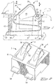
- an electrical connector 2 for connection to a device 1 comprises a pair of terminals 4 mounted in an insulative housing 6.
- the connector 2 is mounted in a device such as a cellular phone, having a casing 15 and a printed circuit board 3.
- the housing 6 extends from a mounting face 8 to a mating face 10, and has terminal receiving cavities 12 extending in a mating direction D for receiving the terminals 4 therein.
- the connector 2 is mountable on the printed circuit board (not shown) where the mounting face 8 is adjacent the printed circuit board, and the mating face 10 facing a complementary connector 3 for mating with the connector 2.
- the complementary connector may be planar contact pads 7 of a rechargeable replaceable battery or other power supply that forms the device 1.
- the free end portion 22 is further provided with a convex abutment surface 48 that abuts an end-wall 50 of the cavity 12 when the contact portion 20 is depressed into the housing.
- the U-bend 24 of the spring portion 18 abuts the opposed end-wall 52 of the cavity 12 such that the contact is guided in a direction transverse to the direction D during depression thereof.
- the contact point 38 moves in a pivoting motion about the U-bend 24, thereby enabling some transverse movement of the contact during coupling.
- the latter provides a wiping action that advantageously removes dirt or oxides on the contact surfaces, which is particularly useful for mating in the direction D.
Landscapes
- Chemical & Material Sciences (AREA)
- Chemical Kinetics & Catalysis (AREA)
- Electrochemistry (AREA)
- General Chemical & Material Sciences (AREA)
- Coupling Device And Connection With Printed Circuit (AREA)
Abstract
Description
- This invention relates to an electrical connector mountable on a printed circuit board and having spring contacts for resiliently contacting a device, in particular a removable rechargeable battery.
- Portable phones and other portable apparatus with rechargeable batteries typically comprise resilient electrical contacts that protrude beyond a mating face of the housing within which they are mounted, and biasable into the housing when the battery device is placed thereon. Due to the relatively large tolerances and frequent coupling and uncoupling of such contacts, they are provided with long spring arms and a great flexibility to absorb large tolerances in positioning, and to ensure operation within the elastic range of the contact. As the spring contacts protrude beyond the mating face quite substantially, external objects may get caught under the contact leading to damage thereof.
- In US-A-5378160 an electrical connector is disclosed comprising a housing having a cavity extending therethrough from a mounting face to a mating face, and a terminal mounted in a cavity, the terminal having a connection portion, a contact portion for contacting a complementary contact, and a supple spring portion extending between the contact and connection portion, the terminal contact portion protruding beyond the mating face.
- A connector system is disclosed in EP-A-0590517 where a base portion of a terminal is secured in a through cavity by interference fit of a barbed portion within the cavity. A resilient contact spring is affixed to the base portion outside the cavity and spans a partition wall. On the other side of the partition wall, a free end portion of the terminal is biased against a surface of the partition wall wall during mating of the connector in order to position the terminal in a direction transverse to the direction of spring biasing of the terminal.
- Due to the supple spring and large travel, it is typical that the contact point travels not only in the direction of mating, but transversely thereto. The transverse movement requires larger contact pads on the portable apparatus. It would be desirable to increase the accuracy of the contact positioning to enable provision of smaller contact pads and to ensure reliable contact.
- In view of the large tolerances in positioning of the complementary contacts, the contact forces of the mating contacts vary significantly. A reasonable minimum force is however desired to ensure reliable electrical contact even if some dirt is present on the contact surfaces. It would be helpful to combine such minimum contact force with a certain wiping action upon mating of the contacts to assist in cleaning the contact surfaces.
- It is also a continuous requirement to provide a cost effective electrical connector for mounting on a printed circuit board. It is further desirable if the connector is as compact as possible, in particular a connector that occupies little space on a circuit board.
- It is an object of this invention to provide an improved electrical connector having supple resilient contacts for connection to contact pads of a complementary device such as a rechargeable battery.
- Objects of this invention have been achieved by providing the connector according to
claim 1. Disclosed herein is an electrical connector comprising a housing having a cavity extending therethrough from a mounting face to a mating face, and a terminal mounted in the cavity, the terminal having a connection portion, a contact portion for contacting a complementary contact, and a supple spring portion extending between the contact and connection portions, the terminal contact portion protruding beyond the mating face, wherein the contact portion is resiliently pivotly attached to the spring portion at one end, and attached to a free end portion at an opposed end, the opposed ends positioned proximate opposed end walls in the housing cavity, wherein upon biasing of the contact in the housing, the free end portion is resiliently biasable against the corresponding cavity end wall for positioning the contact portion in a direction transverse to the direction of spring biasing of the terminal. Also disclosed is an electrical connector for mounting on a PCB, comprising a housing having a cavity extending therethrough from a mounting face to a mating face, and a terminal mounted in the cavity, the terminal having a connection portion, a contact portion for contacting a complementary contact, and a supple spring portion extending between the contact and connection portions, the terminal contact portion protruding beyond the mating face, wherein the terminal connection portion comprises PCB surface mount pads or legs positioned below the housing and attached to the spring section, the connection portion being substantially fully positioned below the housing for minimal use of PCB surface area. Advantageously, a supple, reliable and cost effective spring contact is provided. - Provision of connector walls to guide the transverse movement of the contact point, enables accurate positioning of the contact whilst allowing large spring deflection in the mating direction.
- Provision of locating members at a free end of the contact, for pre-stressing the contact in the uncoupled state, ensures provision of an acceptable minimum contact force, that in combination with the wiping action ensures a good electrical contact with complementary pads.
- Provision of surface mount contact pads or legs below the connector housing, leads to less usage of surface area on the printed circuit board due to provision of the pads below the housing. In addition, the U-shaped bend provides some resilience that reduces local stresses on the solder connection in one embodiment. The latter thus ensures a more secure attachment of the connector to a printed circuit board. In another embodiment, a plurality of spaced apart PCB legs bent orthogonally from the contact base ensure a robust attachment to a PCB.
- Further advantageous features of the invention are described in the claims or will be apparent from following description and the drawings.
- Embodiments of this invention will now be described by way of example, with reference to the accompanying drawings, whereby;
- Figure 1 is a cross-sectional view through a connector according to this invention;
- Figures 2, 3 and 4 are isometric views in different directions of a connector according to this invention;
- Figure 5 is an exploded view of a connector according to this invention;
- Figure 6 is an isometric view of a contact of the connector;
- Figure 7 is a cross-sectional view similar to that of Figure 1 but of a second embodiment;
- Figures 8 and 9 are isometric views of the second embodiment, from a top face and a bottom face respectively; and
- Figure 10 is an isometric view of one of the contacts of the second embodiment.
-
- Referring to Figures 1 and 3, an
electrical connector 2 for connection to a device 1 (partly shown), comprises a pair ofterminals 4 mounted in aninsulative housing 6. Theconnector 2 is mounted in a device such as a cellular phone, having a casing 15 and a printedcircuit board 3. Thehousing 6 extends from amounting face 8 to amating face 10, and has terminal receivingcavities 12 extending in a mating direction D for receiving theterminals 4 therein. Theconnector 2 is mountable on the printed circuit board (not shown) where themounting face 8 is adjacent the printed circuit board, and themating face 10 facing acomplementary connector 3 for mating with theconnector 2. The complementary connector may beplanar contact pads 7 of a rechargeable replaceable battery or other power supply that forms thedevice 1. - Referring to Figures 1 and 6, the
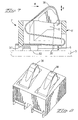
terminal 4 comprises a PCB mounting orconnection portion 14, ahousing retention portion 16, aspring portion 18, acontact portion 20 and afree end portion 22. Theterminal 4 is stamped and formed as a unitary part from sheet metal. - The
spring portion 18 has a generally S-shape comprising two substantially U-shapedbends planar portions contact portion 20 to theattachment portion 16. - The
attachment portion 16 comprisesretention tabs 34 upstanding in the mating direction D of the connector and receivable incomplementary cavities 36 in thehousing 6 in an interference fit. Theretention tabs 34 can be provided with barbs or other such retention features for securely lodging the tabs in thecavity 36, thereby securing the terminals to the housing. Thehousing cavity 12 and retention features 36,34 are adapted in such a manner that theterminal 4 can be inserted into the housing from themounting side 8. The latter enables rapid automated assembly of the terminals to the housing by "stitching" theterminals 4 into thecavities 12 in a single movement, in other words by simply pressing theterminals 4 in the spring compression direction D whereby theretention tabs 34 engage thehousing cavities 36. - The
contact portion 20 is provided with an arcuate shape and acentral embossment 38 forming a contact surface for contacting a complementary pad. - The
free end portion 22 of the contact is provided withpre-stressing engagement members 40 in the shape of a wing (or wings) extending laterally beyond theedges 42 of the free end portion, thewings 40 being engageable with complementary pre-stressingengagement members 44 of the housing in the shape of shoulders recessed into sidewalls of thecavities 12. Upon stitching of theterminal 4 into thecavity 12, thewings 40 engage theshoulders 44 thereby pre-stressing thespring portion 18 of the contact. A minimal spring force is thus provided even if the complementary contact pads only slightly displace thecontact 38 in the direction D. In this embodiment, thecomplementary device 1 is coupled to theconnector 2 by movement thereover in the direction M substantially parallel to theconnector mating face 10. The connector construction would also enable mating in the direction of biasing D of the contact. - The
terminal 4 is further provided withprotection plates 46 that cover a substantial area below thecontact portion 20 that extends beyond themating face 10 in the uncoupled state.Protective plates 46 are provided on either side of the contact and prevent external objects from hooking under thearcuate contact portion 20, thereby preventing damage thereto. Theprotective plates 46 can be integrally provided and bent from thefree end portion 22. - The
free end portion 22 is further provided with aconvex abutment surface 48 that abuts an end-wall 50 of thecavity 12 when thecontact portion 20 is depressed into the housing. The U-bend 24 of thespring portion 18 abuts the opposed end-wall 52 of thecavity 12 such that the contact is guided in a direction transverse to the direction D during depression thereof. Thecontact point 38 moves in a pivoting motion about the U-bend 24, thereby enabling some transverse movement of the contact during coupling. The latter provides a wiping action that advantageously removes dirt or oxides on the contact surfaces, which is particularly useful for mating in the direction D. - Abutment of the free-
end portion 22 against the cavity end-wall 50 ensures that thecontact 38 is positioned in a determined manner for more accurate positioning with respect to complementary contact pads. The abutment also opposes the biasing and sliding forces in the transverse direction M during coupling of thedevice 1, thereby preventing overstressing of thespring section 18. In other words, during transverse sliding of thedevice 1 over thecontact portion 20, thefree end portion 22 abuts thecavity wall 50 and smoothly guides the contact portion in the contact biasing direction D into thehousing cavity 12. Upon retracting thedevice 1, engagement of thepre-stressing wings 40 in the housingcavity sidewall recesses 47 prevents the terminal from overstress, i.e. by thecontact portion 20 being pulled excessively in the direction M thereby pivotly deforming the spring portion of theU-bend 24. - The
mounting portion 14 of the contact extends from thebase plate 30 of thespring portion 18 through aU-bend 54 to a large surfacemount contact pad 56 that is positioned beneath the housing 6 (when looking in the mating direction). The latter arrangement reduces the usage of surface area of a printed circuit board, and additionally the U-bend provides some resiliency in the contact pad with respect to theretention portion 16 to reduce local stress on the solder connection. A furthersurface mount pad 58, stamped and formed from sheet metal, (see Figure 5) is assembled to thehousing 6 at an opposed end to theterminal contact pads 56 for additional mechanical securing of the connector to a printed circuit board. - Referring to Figures 7-10, the second embodiment 2' will now be described. Only the main differences between the connector second embodiment 2' and the
connector 2 of Figures 1-6 will be described, where identical or very similar features are given the same numbering, and different features with the same function given numbers with a prime. The main difference between theconnectors 2, 2' is in thePCB mounting portion 14,14' of thecontact 4,4'. - The mounting or connection portion 14' of the second embodiment 2' comprises surface mount contact legs 56',57' extending in a plane substantially orthogonal to a mounting portion 16' extending from the planar portion 30' of the spring portion 18'. There are a pair of surface mount contact legs 56',57' spaced apart in the slide mating direction M (see Figure 7), which is substantially parallel to the direction of extension of the spring arm 30'. The surface mount contact legs 56',57' are provided extending from opposed lateral edges 59,61 of the substantially planar mounting portion 16'. The contact legs 56',57' raise the mounting portion 16' from the surface of a printed
circuit board 3 abutting against lowerfree edges 63 of the contact legs, such that a gap (G) is provided between the lower spring arm 30' and the PCB. This enables flexing movement of the spring arm towards the PCB to increase the flexibility of thecontact 38 into the housing cavity 12 (i.e. in the biasing direction D). The four contacts legs 56',57' spaced apart from each other provide a very secure and robust mechanical connection to the PCB, as well as an effective electrical connection. The contact legs of the mounting portion 16' are positioned, as in the previous embodiment, substantially below the housing when looking in the direction D of depression of the spring, such that minimal surface area of thePCB 3 is occupied. - The contacts 4' are also stitched into the
cavity 12 of the housing 6', where a retention stud 36' of the housing 6' plugs into a retention member 34' in the form of a cutout in the contact mounting portion 16' in an interference fit.Latches 37' may also be provided on side walls of the housing (see Figure 9) for engaging in the recess 55' between the spaced apart pair of contact legs 56',57'. The contacts 4' can thus be rapidly and simply assembled to the housing 6' by insertion in a single movement and in one direction. The substantially planar mounting portion 16' may be connected to a carrier strip during the stamping and forming process from sheet metal, the contact being severed from the carrier strip at afree end 65 of the mounting portion 16' opposite and remote from anend 67 to which the spring arm 30' is attached. The lateral surface mount legs 56',57' enable theend 65 to be free for connection to the carrier strip which facilitates manufacturing. Other features of the contact 4' such as: the prestressingwings 40 of thefree end portion 22;contact portion 20; U-shaped bends 24,26 of the spring portion; and cooperation of these parts with the housing 6', are largely the same as the previous embodiment and will therefore not be described further.
Claims (13)
- An electrical connector (2,2') comprising a housing (6) having a cavity (12) extending therethrough from a mounting face (8) to a mating face (10), and a terminal (4,4') mounted in the cavity (12), the terminal having a connection portion (14), a contact portion (20) for contacting a complementary contact, and a supple spring portion (18) extending between the contact and connection portions, the terminal contact portion protruding beyond the mating face (10), characterized in that the contact portion (20) is resiliently pivotly attached to the spring portion at one end (24), and attached to a free end portion (22) at an opposed end, the opposed ends positioned proximate opposed end walls (50,52) in the housing cavity (12), wherein upon biasing of the contact portion (20) in the housing, the free end portion is resiliently biasable against the corresponding cavity end wall (50) for positioning the contact portion in a direction transverse to the direction (D) of spring biasing of the terminal.
- The connector of claim 1 wherein the end (24) of the spring portion to which the contact portion is resiliently pivotly attached, abuts the corresponding housing cavity end wall (52) during biasing of the contact portion into the housing cavity (12).
- The connector of claim 1 or 2 wherein the terminal connection portion (14,14') comprises PCB surface mount pads or legs (56,56',57') positioned below the housing (6) and attached to the spring section (18), the connection portion being substantially fully positioned below the housing for minimal use of PCB surface area.
- The connector of any one of claims 1-3 wherein the terminal connection portion (14) comprises PCB surface mount pads (56) positioned below the housing (6) by attachment to the spring section (18) through a U-bend (54).
- The connector of any one of claims 1-3 wherein the terminal connection portion (14') comprises a base extending from an arm (30') of the spring portion (18), and PCB legs (56',57') extending substantially orthogonally from lateral edges (59,61) of the base for surface mount connection to a PCB (3).
- The connector of claim 5 wherein there are a pair of PCB legs (56',57') separated by a recess (55') arranged in the direction of extension of the spring arm (30'), on either edge (59,61).
- The connector of any one of claims 1-6 wherein at least one protective plate (46) is provided below the contact portion to prevent external objects from insertion between the protruding contact portion and connector mating face.
- The connector of claim 7 wherein the protective plate (46) is integrally formed and bent from the contact portion 20.
- The connector of any one of the preceding claims wherein a free end portion (22) at a free end of the contact portion (20) is provided with a pre-stress member (40) engaging a complementary pre-stress member (44) of the housing for pre-stressing the terminal in the uncoupled state.
- The connector of claim 9 wherein the contact pre-stress member (40) is a lateral wing extension (40) that abuts a housing shoulder (44) forming the complementary pre-stress member.
- The connector of any one of the preceding claims wherein the terminal is assembled into the housing cavity (12) from the mounting face in direction (D) of spring biasing of the terminal.
- The connector of claim 11 wherein the terminal comprises a retention tab (34) extending in the terminal spring biasing direction (D) and arranged at one end of the spring portion (18) proximate the connection portion, for insertion into a cavity (36) of the housing in an interference fit.
- The connector of claim 11 wherein the housing is provided with latch members (36',37') that grip onto the terminal mounting portion (14') during assembly, for securing the terminal thereto.
Priority Applications (1)
| Application Number | Priority Date | Filing Date | Title |
|---|---|---|---|
| EP97920906A EP0902994B1 (en) | 1996-05-31 | 1997-05-27 | Rechargeable battery connector |
Applications Claiming Priority (6)
| Application Number | Priority Date | Filing Date | Title |
|---|---|---|---|
| GBGB9611337.8A GB9611337D0 (en) | 1996-05-31 | 1996-05-31 | Rechargable battery connector |
| GB9611337 | 1996-05-31 | ||
| EP96119704 | 1996-12-09 | ||
| EP96119704 | 1996-12-09 | ||
| PCT/IB1997/000593 WO1997045900A1 (en) | 1996-05-31 | 1997-05-27 | Rechargeable battery connector |
| EP97920906A EP0902994B1 (en) | 1996-05-31 | 1997-05-27 | Rechargeable battery connector |
Publications (2)
| Publication Number | Publication Date |
|---|---|
| EP0902994A1 EP0902994A1 (en) | 1999-03-24 |
| EP0902994B1 true EP0902994B1 (en) | 2001-11-28 |
Family
ID=26142353
Family Applications (1)
| Application Number | Title | Priority Date | Filing Date |
|---|---|---|---|
| EP97920906A Expired - Lifetime EP0902994B1 (en) | 1996-05-31 | 1997-05-27 | Rechargeable battery connector |
Country Status (5)
| Country | Link |
|---|---|
| EP (1) | EP0902994B1 (en) |
| JP (1) | JP3923532B2 (en) |
| AU (1) | AU2710897A (en) |
| DE (1) | DE69708625T2 (en) |
| WO (1) | WO1997045900A1 (en) |
Cited By (5)
| Publication number | Priority date | Publication date | Assignee | Title |
|---|---|---|---|---|
| DE10318524B4 (en) * | 2002-05-08 | 2006-06-08 | Tyco Electronics Nederland B.V. | Electrical connector with an abutment surface for a contact spring |
| WO2013020948A1 (en) | 2011-08-09 | 2013-02-14 | Tyco Electronics Amp Gmbh | Electric contact spring, electric spring contact device as well as electric contact zone |
| TWI456821B (en) * | 2009-05-22 | 2014-10-11 | Chi Mei Comm Systems Inc | Battery connector, battery receiving structure and battery |
| US9203172B2 (en) | 2013-02-05 | 2015-12-01 | Tyco Electronics Japan G.K. | Electrical connector assembly and electrical connector used therefor |
| US11271338B2 (en) | 2019-04-25 | 2022-03-08 | Tyco Electronics Japan G.K. | Electrical connection assembly and electrical apparatus |
Families Citing this family (35)
| Publication number | Priority date | Publication date | Assignee | Title |
|---|---|---|---|---|
| EP0924804B1 (en) * | 1997-12-22 | 2003-03-12 | The Whitaker Corporation | Connector with flexible terminals |
| JPH11250966A (en) * | 1997-12-22 | 1999-09-17 | Whitaker Corp:The | connector |
| GB9804333D0 (en) * | 1998-02-27 | 1998-04-22 | Amp Great Britain | Device-to-board electrical connector |
| US5980335A (en) * | 1998-03-27 | 1999-11-09 | Molex Incorporated | Electrical terminal |
| FR2788780B1 (en) * | 1999-01-27 | 2001-03-30 | Ap Cells Inc | PROCESS FOR THE PREPARATION OF MEMBRANE VESICLES |
| JP3286783B2 (en) * | 1999-02-18 | 2002-05-27 | 日本航空電子工業株式会社 | contact |
| JP2001313129A (en) * | 2000-04-28 | 2001-11-09 | Hirose Electric Co Ltd | Stationary device for mounting connection of portable device and electrical connector therefor |
| DE10027600C1 (en) * | 2000-06-02 | 2001-11-22 | Amphenol Tuchel Elect | Contact for mounting in contact bearer has movable part with protruding curved section joined to intermediate section and to hooked section fitting in guide part opening in loaded state |
| EP1168467B1 (en) * | 2000-06-20 | 2011-10-12 | Nxp B.V. | Power supply device of a portable apparatus capable to use different supply types |
| JP4269493B2 (en) * | 2000-07-10 | 2009-05-27 | パナソニック電工株式会社 | Receptacle for battery-powered equipment |
| JP2002093541A (en) * | 2000-09-19 | 2002-03-29 | Miyazaki Oki Electric Co Ltd | IC socket |
| DE20101938U1 (en) | 2001-02-05 | 2001-06-07 | Tyco Electronics Nederland B.V., Hertogenbosch | Resilient contact element and arrangement for resilient contact |
| GB2390755A (en) * | 2002-07-11 | 2004-01-14 | Itt Mfg Enterprises Inc | Spring terminal |
| CN100454670C (en) * | 2002-07-11 | 2009-01-21 | Itt制造企业公司 | Elastic electrical terminal and method of forming same |
| JP4157760B2 (en) | 2002-12-13 | 2008-10-01 | 任天堂株式会社 | Battery connector |
| JP2004265598A (en) * | 2002-12-16 | 2004-09-24 | Iriso Denshi Kogyo Kk | connector |
| JP4273495B2 (en) * | 2004-03-25 | 2009-06-03 | Smk株式会社 | Socket for mounting electronic parts |
| DE102005021039A1 (en) * | 2005-05-06 | 2006-11-09 | Conti Temic Microelectronic Gmbh | Electronic module e.g. for motor vehicle electronics, uses connection elements fitted out as leaf-springs for circuit board |
| JP4684191B2 (en) * | 2006-09-08 | 2011-05-18 | イリソ電子工業株式会社 | connector |
| DE202008001918U1 (en) * | 2008-02-11 | 2009-06-25 | Weidmüller Interface GmbH & Co. KG | In a housing arranged compression spring contact |
| JP5343779B2 (en) * | 2009-09-15 | 2013-11-13 | 住友電装株式会社 | Terminal fitting |
| CN201639002U (en) * | 2009-12-23 | 2010-11-17 | 富士康(昆山)电脑接插件有限公司 | Electrical connectors and their terminals |
| CN102290650B (en) * | 2010-06-21 | 2012-11-28 | 富士康(昆山)电脑接插件有限公司 | Battery connector and assembling method thereof |
| JP5488844B2 (en) * | 2012-01-17 | 2014-05-14 | Smk株式会社 | Pressure contact type connector |
| JP5896786B2 (en) * | 2012-03-02 | 2016-03-30 | 株式会社ヨコオ | Electrical connector |
| JP6469348B2 (en) * | 2014-02-12 | 2019-02-13 | 宏致電子股▲ふん▼有限公司Aces Electronics Co.,Ltd. | Contact terminal structure and connector |
| DE102014006033A1 (en) * | 2014-02-15 | 2015-08-20 | Johnson Electric Germany GmbH & Co. KG | An electrical microswitch comprising at least one electrical contact and method of manufacturing an electrical microswitch |
| JP6684419B2 (en) * | 2016-03-02 | 2020-04-22 | 北川工業株式会社 | contact |
| EP3440902A1 (en) * | 2016-04-04 | 2019-02-13 | Philips Lighting Holding B.V. | Pcb assembly with fasteners |
| WO2018216751A1 (en) * | 2017-05-25 | 2018-11-29 | 株式会社ティー・ピー・エス | Contact |
| JP6745243B2 (en) * | 2017-05-25 | 2020-08-26 | 株式会社T・P・S・クリエーションズ | contact |
| JP7093624B2 (en) * | 2017-12-14 | 2022-06-30 | 株式会社T・P・S・クリエーションズ | contact |
| TWM602744U (en) * | 2020-01-20 | 2020-10-11 | 唐虞企業股份有限公司 | Forced mechanism and connector constituted of the same |
| JP7304838B2 (en) * | 2020-06-29 | 2023-07-07 | 株式会社エスマークスコーポレーション | contact |
| CN117220063A (en) * | 2023-10-30 | 2023-12-12 | 深圳市信维通信股份有限公司 | A kind of elastic connector and electronic equipment |
Family Cites Families (5)
| Publication number | Priority date | Publication date | Assignee | Title |
|---|---|---|---|---|
| JPH0424612Y2 (en) * | 1988-12-09 | 1992-06-10 | ||
| JPH065332A (en) * | 1992-06-22 | 1994-01-14 | Matsushita Electric Ind Co Ltd | Electronic device connection device |
| US5259769A (en) * | 1992-09-29 | 1993-11-09 | Molex Incorporated | Electrical connector with preloaded spring-like terminal with improved wiping action |
| US5378160A (en) * | 1993-10-01 | 1995-01-03 | Bourns, Inc. | Compliant stacking connector for printed circuit boards |
| ZA949398B (en) * | 1993-12-23 | 1995-08-08 | Motorola Inc | Dual beam contact |
-
1997
- 1997-05-27 JP JP54193697A patent/JP3923532B2/en not_active Expired - Fee Related
- 1997-05-27 DE DE69708625T patent/DE69708625T2/en not_active Expired - Fee Related
- 1997-05-27 AU AU27108/97A patent/AU2710897A/en not_active Abandoned
- 1997-05-27 EP EP97920906A patent/EP0902994B1/en not_active Expired - Lifetime
- 1997-05-27 WO PCT/IB1997/000593 patent/WO1997045900A1/en not_active Ceased
Cited By (8)
| Publication number | Priority date | Publication date | Assignee | Title |
|---|---|---|---|---|
| DE10318524B4 (en) * | 2002-05-08 | 2006-06-08 | Tyco Electronics Nederland B.V. | Electrical connector with an abutment surface for a contact spring |
| TWI456821B (en) * | 2009-05-22 | 2014-10-11 | Chi Mei Comm Systems Inc | Battery connector, battery receiving structure and battery |
| WO2013020948A1 (en) | 2011-08-09 | 2013-02-14 | Tyco Electronics Amp Gmbh | Electric contact spring, electric spring contact device as well as electric contact zone |
| DE102011080645A1 (en) | 2011-08-09 | 2013-02-14 | Tyco Electronics Amp Gmbh | ELECTRIC CONTACT SPRING, ELECTRIC SPRING CONTACT DEVICE AND ELECTRIC CONTACT ZONE |
| US9184529B2 (en) | 2011-08-09 | 2015-11-10 | Tyco Electronics Amp Gmbh | Electric contact spring, electric spring contact device as well as electric contact zone |
| EP3361577A1 (en) | 2011-08-09 | 2018-08-15 | TE Connectivity Germany GmbH | Electric contact zone |
| US9203172B2 (en) | 2013-02-05 | 2015-12-01 | Tyco Electronics Japan G.K. | Electrical connector assembly and electrical connector used therefor |
| US11271338B2 (en) | 2019-04-25 | 2022-03-08 | Tyco Electronics Japan G.K. | Electrical connection assembly and electrical apparatus |
Also Published As
| Publication number | Publication date |
|---|---|
| JP2001502837A (en) | 2001-02-27 |
| DE69708625D1 (en) | 2002-01-10 |
| DE69708625T2 (en) | 2002-08-01 |
| AU2710897A (en) | 1998-01-05 |
| EP0902994A1 (en) | 1999-03-24 |
| WO1997045900A1 (en) | 1997-12-04 |
| JP3923532B2 (en) | 2007-06-06 |
Similar Documents
| Publication | Publication Date | Title |
|---|---|---|
| EP0902994B1 (en) | Rechargeable battery connector | |
| EP0590517B1 (en) | Electrical connector with preloaded spring-like terminal with improved wiping action | |
| EP1846990B1 (en) | Board mounted electrical connector | |
| EP1202401B1 (en) | Battery connector | |
| KR970002440B1 (en) | Electrical connector with overstress protection means between housing and contact | |
| US7115005B2 (en) | Electrical connector having resilient contacts | |
| KR100367071B1 (en) | Cordless phone cradle connector | |
| JPH11250966A (en) | connector | |
| US20070298641A1 (en) | Connector assembly | |
| US5716230A (en) | Surface engageable electrical connector | |
| US20080045086A1 (en) | Electrical connector with improved metal spring | |
| US6368156B1 (en) | Audio jack conveniently and reliably mounted on a circuit board | |
| EP0559057B1 (en) | Electrical connector terminal | |
| US7364434B2 (en) | Electrical connector with improved terminal | |
| CN1204170A (en) | floatable connector | |
| CN1178036A (en) | Portable telephone connection system | |
| US6152757A (en) | Electrical connector | |
| US20030045173A1 (en) | Electrical connector assembly with improved contacts | |
| JPH0635418Y2 (en) | connector | |
| US6419501B1 (en) | Connector for flexible printed circuit board | |
| CA1055583A (en) | Telephone line cord adapter | |
| US6767227B2 (en) | Electrical connector | |
| JPS63119156A (en) | Connector for cell | |
| US7077674B2 (en) | Board attachment type electrical connector | |
| JPH11307194A (en) | Connector |
Legal Events
| Date | Code | Title | Description |
|---|---|---|---|
| PUAI | Public reference made under article 153(3) epc to a published international application that has entered the european phase |
Free format text: ORIGINAL CODE: 0009012 |
|
| 17P | Request for examination filed |
Effective date: 19981006 |
|
| AK | Designated contracting states |
Kind code of ref document: A1 Designated state(s): DE FI FR GB SE |
|
| GRAG | Despatch of communication of intention to grant |
Free format text: ORIGINAL CODE: EPIDOS AGRA |
|
| 17Q | First examination report despatched |
Effective date: 20010212 |
|
| GRAG | Despatch of communication of intention to grant |
Free format text: ORIGINAL CODE: EPIDOS AGRA |
|
| GRAH | Despatch of communication of intention to grant a patent |
Free format text: ORIGINAL CODE: EPIDOS IGRA |
|
| GRAH | Despatch of communication of intention to grant a patent |
Free format text: ORIGINAL CODE: EPIDOS IGRA |
|
| GRAA | (expected) grant |
Free format text: ORIGINAL CODE: 0009210 |
|
| AK | Designated contracting states |
Kind code of ref document: B1 Designated state(s): DE FI FR GB SE |
|
| RIC1 | Information provided on ipc code assigned before grant |
Free format text: 7H 01R 12/22 A, 7H 01R 13/24 B |
|
| REG | Reference to a national code |
Ref country code: GB Ref legal event code: IF02 |
|
| REF | Corresponds to: |
Ref document number: 69708625 Country of ref document: DE Date of ref document: 20020110 |
|
| ET | Fr: translation filed | ||
| PLBE | No opposition filed within time limit |
Free format text: ORIGINAL CODE: 0009261 |
|
| STAA | Information on the status of an ep patent application or granted ep patent |
Free format text: STATUS: NO OPPOSITION FILED WITHIN TIME LIMIT |
|
| 26N | No opposition filed | ||
| PGFP | Annual fee paid to national office [announced via postgrant information from national office to epo] |
Ref country code: SE Payment date: 20090528 Year of fee payment: 13 Ref country code: FR Payment date: 20090518 Year of fee payment: 13 Ref country code: FI Payment date: 20090529 Year of fee payment: 13 Ref country code: DE Payment date: 20090528 Year of fee payment: 13 |
|
| PGFP | Annual fee paid to national office [announced via postgrant information from national office to epo] |
Ref country code: GB Payment date: 20090528 Year of fee payment: 13 |
|
| GBPC | Gb: european patent ceased through non-payment of renewal fee |
Effective date: 20100527 |
|
| PG25 | Lapsed in a contracting state [announced via postgrant information from national office to epo] |
Ref country code: FI Free format text: LAPSE BECAUSE OF NON-PAYMENT OF DUE FEES Effective date: 20100527 |
|
| EUG | Se: european patent has lapsed | ||
| REG | Reference to a national code |
Ref country code: FR Ref legal event code: ST Effective date: 20110131 |
|
| PG25 | Lapsed in a contracting state [announced via postgrant information from national office to epo] |
Ref country code: SE Free format text: LAPSE BECAUSE OF NON-PAYMENT OF DUE FEES Effective date: 20100528 |
|
| PG25 | Lapsed in a contracting state [announced via postgrant information from national office to epo] |
Ref country code: DE Free format text: LAPSE BECAUSE OF NON-PAYMENT OF DUE FEES Effective date: 20101201 |
|
| PG25 | Lapsed in a contracting state [announced via postgrant information from national office to epo] |
Ref country code: FR Free format text: LAPSE BECAUSE OF NON-PAYMENT OF DUE FEES Effective date: 20100531 |
|
| PG25 | Lapsed in a contracting state [announced via postgrant information from national office to epo] |
Ref country code: GB Free format text: LAPSE BECAUSE OF NON-PAYMENT OF DUE FEES Effective date: 20100527 |