EP0902459B1 - An apparatus for fabricating a semiconductor device and a method for fabricating a polysilicon film using the same - Google Patents
An apparatus for fabricating a semiconductor device and a method for fabricating a polysilicon film using the same Download PDFInfo
- Publication number
- EP0902459B1 EP0902459B1 EP19970307010 EP97307010A EP0902459B1 EP 0902459 B1 EP0902459 B1 EP 0902459B1 EP 19970307010 EP19970307010 EP 19970307010 EP 97307010 A EP97307010 A EP 97307010A EP 0902459 B1 EP0902459 B1 EP 0902459B1
- Authority
- EP
- European Patent Office
- Prior art keywords
- chamber
- wafer
- cooling
- reaction chamber
- wafer transfer
- Prior art date
- Legal status (The legal status is an assumption and is not a legal conclusion. Google has not performed a legal analysis and makes no representation as to the accuracy of the status listed.)
- Expired - Lifetime
Links
Images


Classifications
-
- H—ELECTRICITY
- H01—ELECTRIC ELEMENTS
- H01L—SEMICONDUCTOR DEVICES NOT COVERED BY CLASS H10
- H01L21/00—Processes or apparatus adapted for the manufacture or treatment of semiconductor or solid state devices or of parts thereof
- H01L21/67—Apparatus specially adapted for handling semiconductor or electric solid state devices during manufacture or treatment thereof; Apparatus specially adapted for handling wafers during manufacture or treatment of semiconductor or electric solid state devices or components ; Apparatus not specifically provided for elsewhere
- H01L21/67005—Apparatus not specifically provided for elsewhere
- H01L21/67011—Apparatus for manufacture or treatment
- H01L21/67155—Apparatus for manufacturing or treating in a plurality of work-stations
- H01L21/6719—Apparatus for manufacturing or treating in a plurality of work-stations characterized by the construction of the processing chambers, e.g. modular processing chambers
-
- H—ELECTRICITY
- H01—ELECTRIC ELEMENTS
- H01L—SEMICONDUCTOR DEVICES NOT COVERED BY CLASS H10
- H01L21/00—Processes or apparatus adapted for the manufacture or treatment of semiconductor or solid state devices or of parts thereof
- H01L21/67—Apparatus specially adapted for handling semiconductor or electric solid state devices during manufacture or treatment thereof; Apparatus specially adapted for handling wafers during manufacture or treatment of semiconductor or electric solid state devices or components ; Apparatus not specifically provided for elsewhere
- H01L21/67005—Apparatus not specifically provided for elsewhere
- H01L21/67011—Apparatus for manufacture or treatment
- H01L21/67098—Apparatus for thermal treatment
- H01L21/67109—Apparatus for thermal treatment mainly by convection
-
- H—ELECTRICITY
- H01—ELECTRIC ELEMENTS
- H01L—SEMICONDUCTOR DEVICES NOT COVERED BY CLASS H10
- H01L28/00—Passive two-terminal components without a potential-jump or surface barrier for integrated circuits; Details thereof; Multistep manufacturing processes therefor
- H01L28/40—Capacitors
- H01L28/60—Electrodes
- H01L28/82—Electrodes with an enlarged surface, e.g. formed by texturisation
- H01L28/84—Electrodes with an enlarged surface, e.g. formed by texturisation being a rough surface, e.g. using hemispherical grains
Definitions
- a cassette chamber in which a carrier having a wafer is loaded, a reaction chamber in which a processing for fabricating a semiconductor device proceeds, and a wafer cooling chamber after completing the processing are respectively connected to a polyhedral transfer chamber having a robot arm for transferring the wafer to the respective chambers.
- the wafer for forming the polysilicon film is loaded in the cassette chamber 200.
- the robot arm 212 places the wafer on the susceptor 394 in the reaction chamber 220 through the wafer transfer chamber 210. Then, the temperature of the reaction chamber 220 is raised to a certain temperature by the heater 390 in the heating block 392.
Description
- To manufacture a reliable semiconductor device, it is required to keep the temperature of the apparatus for fabricating the semiconductor device uniform and to minimize the contaminant particles.
- Especially, in the case of forming a lower electrode with a hemispherical silicon grain (which is referred to as HSG-Si) to enlarge the electrostatic capacitance of a capacitor in terms of increasing the area of the lower electrode, it is critical to keep the temperature of the reaction chamber uniform and to keep the inside of the reaction chamber clean.
- Typically, to form the lower electrode with the HSG-Si, a crystal growing step for forming crystal grains by migrating the amorphous silicon to the nucleus of crystalline silicon needs to be stable and a speed of silicon surface migration for the growth of the crystal grain needs to be faster than the speed of the amorphous silicon crystallization in lower amorphous silicon. For the amorphous silicon to move toward the nucleus of the crystalline silicon, the amorphous silicon should have a free surface on which the silicon atoms of the surface are not combined to any other atoms. Namely, when the surface is contaminated with other materials, the surface movement of the amorphous silicon atoms gets hard since the amorphous silicon atoms are combined to the atoms of the other materials, thus making any further generation and growth of nucleus impossible. Therefore, to remove the contaminants of the wafer surface transferred to the reaction chamber and to keep the inside of the chamber clean are important factors in a processing.
- An article in Solid State Technology, Vol 37, No. 12, December 1994, pages 45-49 by Katherine Derbyshire describes multichamber processing in which two or more vacuum process chambers are attached to a single wafer handler. A system is described in which a wafer transfer chamber is connected to a cassette chamber for loading a semiconductor wafer, a reaction chamber and a wafer cooling chamber.
- In a general apparatus for fabricating the semiconductor device, a cassette chamber in which a carrier having a wafer is loaded, a reaction chamber in which a processing for fabricating a semiconductor device proceeds, and a wafer cooling chamber after completing the processing are respectively connected to a polyhedral transfer chamber having a robot arm for transferring the wafer to the respective chambers.
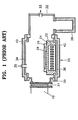
- The structure of the reaction chamber in which the processing for fabricating the device proceeds is described as follows with reference to FIG. 1. A
gate valve 31 which separates awafer transfer chamber 10 and areaction chamber 20 is equipped between thefirst side wall 30 of the reaction chamber and thewafer transfer chamber 10, and agas vent opening 33 is formed on asecond side wall 32 opposite to thefirst side wall 30. A gas injectopening 35 is formed to pass through anupper wall 34 of the reaction chamber and acooling jacket 40 installed on it. Acooling jacket 42 is installed outside of abottom wall 36 of the reaction chamber. Aheating block 24 having aheater 22 and asusceptor 26 for sustaining awafer 28 on theheating block 24 are installed inside of thereaction chamber 20. Also, aturbo pump 38 is connected to thesecond side wall 32 on which thegas vent opening 33 is formed. - In the case of proceeding the processing using the conventional semiconductor device fabricating apparatus shown in FIG. 1, the following problems occur.
- First, the wafer is transferred to the
reaction chamber 20 right after being transferred from the cassette chamber (not shown) to thewafer transfer chamber 10 by the robot arm. The pressure of the cassette chamber at the beginning of the transfer is about 1mtorr (1 torr = 133 Pa). Therefore, air pollution gas of about 1mtorr is transferred from the cassette chamber to the wafer transfer chamber when the wafer is transferred. Therefore, the wafer transfer chamber is contaminated with the air pollution gas though having a low pressure. As a result, thereaction chamber 20 connected to thewafer transfer chamber 10 is also contaminated with the air pollution gas. Therefore, the surface of the wafer is contaminated by the air pollution gas such as moisture and carbon compound during the process of raising the temperature of thewafer 28 in thereaction chamber 20, thus reducing the reliability of the processing. Especially, in the case of forming the lower electrode with the HSG-Si, it is impossible to increase the surface area since the speed of the surface migration of the amorphous silicon is reduced by adsorption of contaminants to the amorphous silicon. - Second, the surface of the
wafer 28 is cleaned to remove an organic material or a native oxide film existing on the surface of the wafer prior to the processing in thereaction chamber 20. Therefore, a certain amount of moisture exists on the surface of thewafer 28 which is loaded in the cassette chamber (not shown) and the moisture is not completely evaporized and removed in the cassette chamber under the pressure of 1mtorr. Therefore, vapor is continuously generated when thewafer 28 is transferred from thewafer transfer chamber 10 to thereaction chamber 20. Especially in a process for forming the HSG-Si, the speed of the surface migration of the amorphous silicon is reduced by the vapor which is continuously generated. Thus, the increase of the surface area is also reduced. - Third, in the case of injecting cooling gas such as argon or helium of 1 to 100 torr to the cooling chamber (not shown), the cooling gas flows into the
wafer transfer chamber 10 connected to the cooling chamber. The cooling gas which has flown into thewafer transfer chamber 10 reflows into thereaction chamber 20, thus acting as a contaminant. Namely, the speed of the surface migration of the amorphous silicon is reduced since the surface of thewafer 28 is contaminated by the cooling gas. - Fourth, as shown in FIG. 1, the reaction chamber includes the
cooling jackets bottom walls gate valve 31 separating thetransfer chamber 10 and thereaction chamber 20, thefirst side wall 30 adjacent to thegate valve 31 and thesecond side wall 32 opposite to thefirst side wall 30 reaches approximately 50°C and higher, since the above three portions have no cooling jackets. Thus, the surface contaminants existing in the chamber walls and the wafer may exude in the gas form. Therefore, a shortcoming is generated in the process implemented in thereaction chamber 20 due to the gas exuded from thegate valve 31, thefirst side wall 30, and thesecond side wall 32. Especially in the case of the processing for forming the HSG-Si, it is impossible to achieve the desired surface increase effect since the exuded gas is adsorbed to the surface of the silicon. - The present invention provides a semiconductor device fabricating apparatus comprising:
- a cassette chamber for loading a semiconductor wafer;
- a wafer transfer chamber having a front portion connected to the cassette chamber;
- a reaction chamber connected to a rear portion of the wafer transfer chamber, the reaction chamber having first to fourth cooling jackets mounted on a first side wall adjacent to the wafer transfer chamber, a second side wall opposite to the first side wall, an upper wall, and a bottom wall, respectively; and
- a wafer cooling chamber connected to a side portion of the wafer transfer chamber.
-
- The present invention also provides a method according to
claim 4. Preferred embodiments are defined in the dependent claims. - Examples of the present invention will now be described in detail with reference to the accompanying drawings, in which:
- FIG. 1 is a sectional view of a reaction chamber of a conventional semiconductor device fabricating apparatus;
- FIG. 2 is a plan view of a semiconductor device fabricating apparatus according to an embodiment of the present invention;
- FIG. 3 is a sectional view of the reaction chamber taken along the line III-III' of FIG. 2;
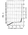
- FIG. 4 is a graph showing the relation between pumping down time and cassette chamber pressure;
- FIGS. 5A to 5E are scanning electron microscope photographs of the surface of a capacitor lower electrode formed by a method for fabricating a polysilicon film according to an embodiment of the present invention and formed in the positions of the wafer shown in FIG. 5F;
- FIGS. 6A and 6B are scanning electron microscope photographs of the surface of the capacitor lower electrode formed by a conventional semiconductor device fabricating apparatus, as a contrast group to the first embodiment;
- FIG. 7A is a scanning electron microscope photograph of the surface of the capacitor lower electrode formed by a further method for fabricating a polysilicon film;
- FIG. 7B is a scanning electron microscope photograph of the surface of the capacitor lower electrode formed by a conventional silicon film fabricating method, as a contrast group to the previous method;
- FIG. 8 is a bar graph showing the value of the maximum capacitance of the capacitor shown in FIGS. 7A and 7B;
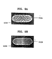
- FIG. 9A is a scanning electron microscope photograph of the surface of the capacitor lower electrode formed by a further polysilicon film fabricating method;
- FIG. 9B is a scanning electron microscope photograph of the surface of the capacitor lower electrode formed by a conventional polysilicon film fabricating method, as a contrast group to the previous method;
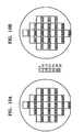
- FIG 10A shows the capacitances of the respective portions of the wafer after forming the capacitor lower electrode by a further polysilicon film fabricating method;
- FIG. 10B shows the capacitance of the capacitor lower electrode formed by the conventional polysilicon film fabricating method, as a contrast group to the previous method; and
- FIG. 11 is a graph showing the reproductivity of the process in the case of forming the capacitor by the previous polysilicon film fabricating method.
-
- Referring to FIG. 2, the semiconductor device fabricating apparatus according to the embodiment of the present invention includes a
cassette chamber 200, which acarrier 202 having awafer 204 is loaded in and separates thecarrier 202 from atmosphere, awafer transfer chamber 210 having arobot arm 212 for transferring thewafer 204 to areaction chamber 220, thereaction chamber 220 in which a processing for fabricating a semiconductor device proceeds, and awafer cooling chamber 230 for cooling the wafer after completing the processing. - Five cooling jackets are installed in the
reaction chamber 220 according to the embodiment of the present invention. They are described in detail with reference to FIG. 3 showing an amplified sectional view of thereaction chamber 220 taken along the line III-III' of FIG. 2. - Referring to FIG. 3, a gate valve 310 for separating the
wafer transfer chamber 210 from thereaction chamber 220 is formed on afirst side wall 300 and afirst cooling jacket 400 and asecond cooling jacket 410 are respectively formed on afirst side wall 300 and asecond side wall 320. A gas inject opening 350 is formed to pass through an upper wall of thereaction chamber 340 and athird cooling jacket 420 formed on the upper end wall of thereaction chamber 340. Afourth cooling jacket 430 is also formed outside of abottom wall 360 of the reaction chamber. Aheating block 392 having aheater 390 inside of thereaction chamber 220 and asusceptor 394 for sustain thewafer 204 on theheating block 392. Aturbo pump 380 is connected to thesecond side wall 320 on which a gas vent opening 330 is formed and afifth cooling jacket 440 is formed on the surface of the gate valve 310. - A refrigerant selected from the group consisting of a cooling water and a mixture of the cooling water and ethylene glycol is preferably used in the first to the
fifth cooling jackets reaction chamber 220 substantially less than 10°C. - In the semiconductor device fabricating apparatus according to the present invention, the cooling jackets are installed on walls other than the upper and bottom walls of the reaction chamber. Therefore, it is possible to prevent gas from being exuded from the chamber walls by supplying the refrigerant to the respective cooling jackets during the processing in the reaction chamber.
- In an embodiment of the method of the present invention, the polysilicon film is fabricated using the reaction chamber shown in FIG. 3. The embodiment is described below.
- First, the wafer for forming the polysilicon film is loaded in the
cassette chamber 200. Continuously, therobot arm 212 places the wafer on thesusceptor 394 in thereaction chamber 220 through thewafer transfer chamber 210. Then, the temperature of thereaction chamber 220 is raised to a certain temperature by theheater 390 in theheating block 392. - Then, the amorphous silicon film is formed to a predetermined thickness on the wafer using the gas selected from the group consisting of silane, disilane, and the gas mixture in which silane and disilane are mixed in the 30:1 to 1:30 ratio as the source gas. The polysilicon film is completed by forming the HSG-Si by performing the thermal treatment on the wafer on which the amorphous silicon film is formed. The polysilicon film is preferably used as a lower electrode of the capacitor.
- When the processing proceeds in the reaction chamber, the problem that gas is exuded from the walls of the cooling chamber is prevented by supplying the refrigerant to the first to
fifth cooling jackets - The characteristic of the present invention is illustrated with reference to the following example 1.
- A wafer on which an insulating layer with a contact hole exposing a source region have been already formed is loaded on a
susceptor 394 in the semiconductor device fabricating apparatus according to an embodiment of the present invention shown in FIG. 3. The capacitor having enlarged surface area is fabricated by forming an amorphous silicon layer to the thickness of 3000Å (10Å = 1nm) by flowing the disilane gas and then, forming the HSG-Si by flowing the disilane gas with a flow rate of 18sccm, on the surface of the amorphous silicon layer controlling the temperature of wafer to 620°C. During the above processing, the temperature of the walls of the wafer cooling chamber is kept to be 10°C by flowing the refrigerant of 9°C into the first to thefifth cooling jackets Reference numerals Reference numerals - To clearly check the prevention effect of the gas exudation of the semiconductor device fabricating apparatus according to the present invention, the lower electrode of the capacitor is also formed in the conventional semiconductor device fabricating apparatus shown in FIG. 1 after controlling the processing condition such as reaction gas and temperature to be equal to that used when forming the electrode in the apparatus according to an embodiment of the present invention, as a contrast group. The scanning electron microscope photographs of the lower electrodes of a contrast group are shown in FIGS. 6A and 6B. FIGS. 6A and 6B respectively show the lower electrode formed in the reaction chamber which is adjacent to the wafer transfer chamber and the lower electrode formed in the reaction chamber which is adjacent to a vent portion. The
reference numerals reference numerals - When the lower electrode of the capacitor is formed using the semiconductor device fabricating apparatus according to the present invention, the temperature of the walls of the reaction chamber, especially, the gate valve 310, the
first wall 300 to which the gate valve 310 is connected, and thesecond wall 320 on which the vent portion is formed can be kept low. Therefore, the problem that the formation of the surface flection degrades as the speed of the surface movement decreases due to the exuded gas is overcome since the gas exudation from the chamber walls is prevented. - The following further examples illustrate the effect of pressure control in the various chambers.
- To examine the relations between the pressure of the cassette chamber and the pressure of the wafer transfer chamber and between the pressure of the cassette chamber and the pressure of the reaction chamber, the pressure between the respective chambers are measured.
a cassette chamber a wafer transfer chamber a reaction chamber initial pressure changed pressure initial pressure changed pressure a contrast 0.1mtorr 0.23µtorr 2.2µtorr 7.3ntorr 20ntorr group an experimental group 0.02mtorr 0.23µtorr 0.23µtorr 7.3ntorr 13ntorr - As noted from the results of the experimental group, in the case of controlling the pressure of the cassette chamber to be 0.02mtorr, even though the gate valves between the cassette chamber and the wafer transfer chamber and between the cassette chamber and the reaction chamber are opened, the pressure in the respective chambers does not increase.
- The lower electrode with the HSG-Si is also formed by depositing the amorphous silicon film by controlling the pressure of the cassette chamber to be 0.05mtorr and flowing the disilane at a flow rate of 18sccm as a source gas and controlling the temperature of the wafer to be 620°C. The photograph of the surface of the lower electrode with the scanning electron microscope is shown in FIG. 7A. The scanning electron microscope photograph of the lower electrode formed by controlling the pressure of the cassette chamber to be 0.1mtorr and controlling the other conditions to be equal to those of the experimental group in Table 1 as a comparing group for comparing with the result of the experimental group is shown in FIG. 7B. The
reference numerals reference numerals - As noted from FIG. 7A, while it is possible to form a uniform HSG-Si on the surface of the lower electrode in the case of controlling the pressure of the cassette chamber to be 0.05mtorr according to the present invention, the degradation of the surface flection is generated as shown from FIG. 7B by the contaminant of the atmosphere and the evaporized vapor from the wafer in the case of controlling the pressure of the cassette chamber to be high as in the conventional technology.
- FIG. 8 is a bar graph showing the value of measuring the maximum capacitance of the capacitor shown in FIGS. 7A and 7B. This result shows the mean value of the maximum capacitance measured from 10 wafers. As noted from the graph, the capacitance of the capacitor of Figure 7A is 65(fF/cell), which is twice that of the capacitor formed by the conventional technology, i.e., 30(fF/cell).
- To examine the relations between the pressure of the cooling chamber and the pressure of the wafer transfer chamber and between the pressure of the cooling chamber and the pressure of the reaction chamber, the pressure between the respective chambers are measured.
a wafer cooling chamber a wafer transfer chamber reaction chamber initial pressure changed pressure initial pressure changed pressure a contrast group 240 mtorr 0.25µtorr 2.3µtorr 7.3ntorr 2.3µtorr an experimental group 1µtorr 0.25µtorr 0.25µtorr 7.3ntorr 15ntorr - As noted from the results of the contrast group, in the case of cooling the wafer in the wafer cooling chamber, the cooling gas raises the pressure of the wafer transfer chamber (0.25µtorr→2.3µtorr) and, in the case of transferring the wafer to the reaction chamber to perform another processing to the wafer in the above state, the cooling gas also raises the pressure of the reaction chamber (7.3ntorr→2.3µtorr). Such an increase of the pressure causes to contaminate the surface of the wafer in the case of raising the temperature of the transferred wafer. Therefore, in the case of cooling the wafer in the wafer cooling chamber under the pressure which is equal to that of the wafer transfer chamber, i.e., 1µtorr without using the cooling gas like in the experimental group, there is little change of the pressure in the wafer transfer chamber and the reaction chamber, thus suppressing the contamination of the reaction chamber.
- The scanning electron microscope photograph of the surface of the lower electrode in which the HSG-Si is formed by depositing the amorphous silicon film by controlling the pressure of the wafer cooling chamber and the wafer transfer chamber to be 1µtorr and flowing the disilane at a flow rate of 18sccm as a source gas and controlling the temperature of the wafer to be 620°C is shown in FIG. 8A. The scanning electron microscope photograph of the lower electrode formed by injecting argon of the pressure of 240mtorr as the cooling gas and controlling the other conditions to be equal to those of the experimental group shown in Table 2 as a comparing group is shown in FIG. 9B. The
reference numerals reference numerals - It is noted from the result of FIG. 9A that a flection is uniformly formed on the surface of the amorphous silicon when the pressure of the wafer cooling chamber and the wafer transfer chamber are equally kept under 1µtorr. It is also noted from the result of FIG. 9B that it is impossible to obtain a desirable surface flection effect due to the reduction of the speed of the surface migration of the amorphous silicon atoms to the crystalline silicon when the wafer is cooled in the wafer cooling chamber using the cooling gas and the pressure of the wafer cooling chamber is higher than 1µtorr.
- The result of measuring the capacitances of the respective portions of the wafer after forming the lower electrode of the capacitor by controlling the pressure of the cassette chamber to be 0.05mtorr and that of the wafer cooling chamber and the wafer transfer chamber to be less than 1µtorr and controlling the other conditions to be equal to those of the example 1 is shown in FIG. 10A. The capacitances of the respective portions of the wafer after forming the lower electrode of the capacitor by a conventional processing condition using the conventional apparatus is shown in FIG. 10B. The numbers in the respective blocks denote the capacitances. It is noted from FIGS. 10A and 10B that the lower electrodes have a uniform capacitance through the whole surface of the wafer when the lower electrode of the capacitor is according to the conditions specified for Figure 10A.
- FIG. 11 is a graph showing the capacitance measured after continuously performing the processings on the five wafers according to the fourth example, showing the result that the capacitance is uniform, namely, the reproduction is high compared with the conventional apparatus and method even though the processings continuously proceed.
- In particular, when the reaction chamber includes the cooling jacket according to the apparatus of the present invention, the reliability to the processing performance is improved since it is possible to prevent gas from being exuded in the reaction chamber.
Claims (10)
- A semiconductor device fabricating apparatus, comprising:a cassette chamber (200) for loading a semiconductor wafer;a wafer transfer chamber (210) having a front portion connected to the cassette chamber (200);a reaction chamber (220) connected to a rear portion of the wafer transfer.chamber (210); and a wafer cooling chamber (230) connected to a side portion of the wafer transfer chamber (210); characterised in that the reaction chamber (220) has first to fourth cooling jackets (400,410,420,430) mounted on a first side wall (300) adjacent to the wafer transfer chamber (210), a second side wall (320) opposite to the first side wall (300), an upper wall (340), and a bottom wall (360), respectively.
- The apparatus of claim 1, further comprising:a gate valve (310) located between the reaction chamber (220) and the wafer transfer chamber (210) for separating the reaction chamber (220) from the wafer transfer chamber (210), the gate valve (310) having a fifth cooling jacket (440).
- The apparatus of claim 2, wherein each of first (400), second (410), third (420), and fifth (440) cooling jackets has a refrigerant selected from the group consisting of cooling water and mixture of the cooling water and ethylene glycol.
- A method of fabricating a polysilicon film in the apparatus according to claim 1, comprising the steps of:loading a wafer for forming a polysilicon film in the cassette chamber;transferring the loaded wafer to the reaction chamber through the wafer transfer chamber;flowing refrigerant into the first to fourth cooling jackets;forming an amorphous silicon film on the wafer by injecting into the reaction chamber gas selected from silane, disilane, and a silane-disilane gas mixture in which the silane: disilane ratio ranges from 30:1 to 1:30;transforming the amorphous silicon film into a polysilicon film on which HSG-Si is formed by thermally treating the wafer having the amorphous silicon film; andtransferring the wafer on which the HSG-Si is formed to the cooling chamber and cooling it.
- The method of claim 4, wherein the temperature of the refrigerant is substantially less than 9°C.
- The method of claim 4, wherein the polysilicon film is a lower electrode of a capacitor.
- The method of claim 4, wherein the pressure of the cassette chamber is adjusted to be less than 6.67x10³ Pa (0.05mtorr).
- The method of claim 4 or 6, wherein the pressure of the cassette chamber is adjusted by pumping down for ten to thirty minutes.
- The method of claim 4, wherein the pressure of the cooling chamber and the wafer transfer chamber is adjusted to be equal.
- The method of claim 9, wherein the pressure of the cooling chamber and the wafer transfer chamber is adjusted to be less than 133x106Pa (1.0µtorr).
Priority Applications (3)
| Application Number | Priority Date | Filing Date | Title |
|---|---|---|---|
| EP04076537A EP1455384A3 (en) | 1997-09-10 | 1997-09-10 | An apparatus for fabricating a semiconductor device and a method for fabricating a polysilicon film using the same |
| EP19970307010 EP0902459B1 (en) | 1997-09-10 | 1997-09-10 | An apparatus for fabricating a semiconductor device and a method for fabricating a polysilicon film using the same |
| DE1997634877 DE69734877T2 (en) | 1997-09-10 | 1997-09-10 | Device for producing a semiconductor device and a method for producing a polysilicon layer using this device |
Applications Claiming Priority (1)
| Application Number | Priority Date | Filing Date | Title |
|---|---|---|---|
| EP19970307010 EP0902459B1 (en) | 1997-09-10 | 1997-09-10 | An apparatus for fabricating a semiconductor device and a method for fabricating a polysilicon film using the same |
Related Child Applications (1)
| Application Number | Title | Priority Date | Filing Date |
|---|---|---|---|
| EP04076537A Division EP1455384A3 (en) | 1997-09-10 | 1997-09-10 | An apparatus for fabricating a semiconductor device and a method for fabricating a polysilicon film using the same |
Publications (2)
| Publication Number | Publication Date |
|---|---|
| EP0902459A1 EP0902459A1 (en) | 1999-03-17 |
| EP0902459B1 true EP0902459B1 (en) | 2005-12-14 |
Family
ID=8229504
Family Applications (2)
| Application Number | Title | Priority Date | Filing Date |
|---|---|---|---|
| EP04076537A Withdrawn EP1455384A3 (en) | 1997-09-10 | 1997-09-10 | An apparatus for fabricating a semiconductor device and a method for fabricating a polysilicon film using the same |
| EP19970307010 Expired - Lifetime EP0902459B1 (en) | 1997-09-10 | 1997-09-10 | An apparatus for fabricating a semiconductor device and a method for fabricating a polysilicon film using the same |
Family Applications Before (1)
| Application Number | Title | Priority Date | Filing Date |
|---|---|---|---|
| EP04076537A Withdrawn EP1455384A3 (en) | 1997-09-10 | 1997-09-10 | An apparatus for fabricating a semiconductor device and a method for fabricating a polysilicon film using the same |
Country Status (2)
| Country | Link |
|---|---|
| EP (2) | EP1455384A3 (en) |
| DE (1) | DE69734877T2 (en) |
Family Cites Families (5)
| Publication number | Priority date | Publication date | Assignee | Title |
|---|---|---|---|---|
| US5254170A (en) * | 1989-08-07 | 1993-10-19 | Asm Vt, Inc. | Enhanced vertical thermal reactor system |
| US5516732A (en) * | 1992-12-04 | 1996-05-14 | Sony Corporation | Wafer processing machine vacuum front end method and apparatus |
| EP0608633B1 (en) * | 1993-01-28 | 1999-03-03 | Applied Materials, Inc. | Method for multilayer CVD processing in a single chamber |
| JP2833545B2 (en) * | 1995-03-06 | 1998-12-09 | 日本電気株式会社 | Method for manufacturing semiconductor device |
| US5663090A (en) * | 1995-06-29 | 1997-09-02 | Micron Technology, Inc. | Method to thermally form hemispherical grain (HSG) silicon to enhance capacitance for application in high density DRAMs |
-
1997
- 1997-09-10 EP EP04076537A patent/EP1455384A3/en not_active Withdrawn
- 1997-09-10 EP EP19970307010 patent/EP0902459B1/en not_active Expired - Lifetime
- 1997-09-10 DE DE1997634877 patent/DE69734877T2/en not_active Expired - Fee Related
Also Published As
| Publication number | Publication date |
|---|---|
| EP1455384A3 (en) | 2004-10-20 |
| DE69734877D1 (en) | 2006-01-19 |
| EP0902459A1 (en) | 1999-03-17 |
| DE69734877T2 (en) | 2006-09-14 |
| EP1455384A2 (en) | 2004-09-08 |
Similar Documents
| Publication | Publication Date | Title |
|---|---|---|
| US6039811A (en) | Apparatus for fabricating polysilicon film for semiconductor device | |
| JP3676983B2 (en) | Semiconductor manufacturing method, substrate processing method, and semiconductor manufacturing apparatus | |
| US5629043A (en) | Silicon nitride film formation method | |
| US4985372A (en) | Method of forming conductive layer including removal of native oxide | |
| US4956204A (en) | Process of forming a film by low pressure chemical vapor deposition | |
| JP2892170B2 (en) | Heat treatment film formation method | |
| KR100299784B1 (en) | A method for forming a textured polysilicon layer, a substrate processing apparatus used to implement this method, and a semiconductor memory device | |
| JP3741518B2 (en) | Method for manufacturing capacitor lower electrode of semiconductor memory device | |
| US6350321B1 (en) | UHV horizontal hot wall cluster CVD/growth design | |
| EP0902459B1 (en) | An apparatus for fabricating a semiconductor device and a method for fabricating a polysilicon film using the same | |
| JP5355514B2 (en) | Semiconductor manufacturing method, substrate processing method, and substrate processing apparatus | |
| JP4669257B2 (en) | Semiconductor manufacturing method, substrate processing method, and substrate processing apparatus | |
| EP0902462B1 (en) | A method for manufacturing a capacitor lower electrode of a semiconductor memory device | |
| JP4240941B2 (en) | Semiconductor device manufacturing method and substrate processing apparatus | |
| KR100331964B1 (en) | Equpiment for for depositing atom layer and method for depositing thereof | |
| JP4456341B2 (en) | Semiconductor device manufacturing method and substrate processing apparatus | |
| US6780250B2 (en) | System and method for integrated oxide removal and processing of a semiconductor wafer | |
| US6194292B1 (en) | Method of fabricating in-situ doped rough polycrystalline silicon using a single wafer reactor | |
| JPH09129626A (en) | Formation of thin film | |
| US6066538A (en) | Methods and apparatus for forming integrated circuit capacitors having composite oxide-nitride-oxide dielectric layers therein | |
| KR19990013845A (en) | Manufacturing Method of Semiconductor Device | |
| JP2002222871A (en) | Method for heat treatment | |
| KR100238205B1 (en) | Fabrication Method for Polysilicon layer having HSG-Si thereon | |
| KR20010018996A (en) | Method for controlling a wafer in a single wafer type apparatus for manufacturing a semiconductor device | |
| JPH10173130A (en) | Capacitive element and method of forming the same |
Legal Events
| Date | Code | Title | Description |
|---|---|---|---|
| PUAI | Public reference made under article 153(3) epc to a published international application that has entered the european phase |
Free format text: ORIGINAL CODE: 0009012 |
|
| 17P | Request for examination filed |
Effective date: 19970917 |
|
| AK | Designated contracting states |
Kind code of ref document: A1 Designated state(s): DE FR GB NL |
|
| AX | Request for extension of the european patent |
Free format text: AL;LT;LV;RO;SI |
|
| AKX | Designation fees paid |
Free format text: DE FR GB NL |
|
| 17Q | First examination report despatched |
Effective date: 20031006 |
|
| GRAP | Despatch of communication of intention to grant a patent |
Free format text: ORIGINAL CODE: EPIDOSNIGR1 |
|
| GRAS | Grant fee paid |
Free format text: ORIGINAL CODE: EPIDOSNIGR3 |
|
| GRAA | (expected) grant |
Free format text: ORIGINAL CODE: 0009210 |
|
| AK | Designated contracting states |
Kind code of ref document: B1 Designated state(s): DE FR GB NL |
|
| REG | Reference to a national code |
Ref country code: GB Ref legal event code: FG4D |
|
| REF | Corresponds to: |
Ref document number: 69734877 Country of ref document: DE Date of ref document: 20060119 Kind code of ref document: P |
|
| PLBE | No opposition filed within time limit |
Free format text: ORIGINAL CODE: 0009261 |
|
| STAA | Information on the status of an ep patent application or granted ep patent |
Free format text: STATUS: NO OPPOSITION FILED WITHIN TIME LIMIT |
|
| 26N | No opposition filed |
Effective date: 20060915 |
|
| EN | Fr: translation not filed | ||
| ET | Fr: translation filed | ||
| REG | Reference to a national code |
Ref country code: FR Ref legal event code: EERR Free format text: CORRECTION DE BOPI 07/05 - BREVETS EUROPEENS DONT LA TRADUCTION N A PAS ETE REMISE A L INPI. IL Y A LIEU DE SUPPRIMER : LA MENTION DE LA NON REMISE. LA REMISE DE LA TRADUCTION EST PUBLIEE DANS LE PRESENT BOPI. |
|
| PGFP | Annual fee paid to national office [announced via postgrant information from national office to epo] |
Ref country code: NL Payment date: 20080903 Year of fee payment: 12 Ref country code: FR Payment date: 20080915 Year of fee payment: 12 |
|
| PGFP | Annual fee paid to national office [announced via postgrant information from national office to epo] |
Ref country code: GB Payment date: 20080910 Year of fee payment: 12 |
|
| PGFP | Annual fee paid to national office [announced via postgrant information from national office to epo] |
Ref country code: DE Payment date: 20080926 Year of fee payment: 12 |
|
| REG | Reference to a national code |
Ref country code: NL Ref legal event code: V1 Effective date: 20100401 |
|
| GBPC | Gb: european patent ceased through non-payment of renewal fee |
Effective date: 20090910 |
|
| REG | Reference to a national code |
Ref country code: FR Ref legal event code: ST Effective date: 20100531 |
|
| PG25 | Lapsed in a contracting state [announced via postgrant information from national office to epo] |
Ref country code: NL Free format text: LAPSE BECAUSE OF NON-PAYMENT OF DUE FEES Effective date: 20100401 Ref country code: FR Free format text: LAPSE BECAUSE OF NON-PAYMENT OF DUE FEES Effective date: 20090930 Ref country code: DE Free format text: LAPSE BECAUSE OF NON-PAYMENT OF DUE FEES Effective date: 20100401 |
|
| PG25 | Lapsed in a contracting state [announced via postgrant information from national office to epo] |
Ref country code: GB Free format text: LAPSE BECAUSE OF NON-PAYMENT OF DUE FEES Effective date: 20090910 |