EP0902297A3 - Adapter devices for testing printed circuit boards - Google Patents
Adapter devices for testing printed circuit boards Download PDFInfo
- Publication number
- EP0902297A3 EP0902297A3 EP98116790A EP98116790A EP0902297A3 EP 0902297 A3 EP0902297 A3 EP 0902297A3 EP 98116790 A EP98116790 A EP 98116790A EP 98116790 A EP98116790 A EP 98116790A EP 0902297 A3 EP0902297 A3 EP 0902297A3
- Authority
- EP
- European Patent Office
- Prior art keywords
- contact
- film
- printed circuit
- test
- point
- Prior art date
- Legal status (The legal status is an assumption and is not a legal conclusion. Google has not performed a legal analysis and makes no representation as to the accuracy of the status listed.)
- Withdrawn
Links
- 239000004020 conductor Substances 0.000 abstract 1
- 239000011810 insulating material Substances 0.000 abstract 1
- 238000007747 plating Methods 0.000 abstract 1
- 239000002356 single layer Substances 0.000 abstract 1
Classifications
-
- H—ELECTRICITY
- H05—ELECTRIC TECHNIQUES NOT OTHERWISE PROVIDED FOR
- H05K—PRINTED CIRCUITS; CASINGS OR CONSTRUCTIONAL DETAILS OF ELECTRIC APPARATUS; MANUFACTURE OF ASSEMBLAGES OF ELECTRICAL COMPONENTS
- H05K3/00—Apparatus or processes for manufacturing printed circuits
- H05K3/36—Assembling printed circuits with other printed circuits
- H05K3/361—Assembling flexible printed circuits with other printed circuits
- H05K3/365—Assembling flexible printed circuits with other printed circuits by abutting, i.e. without alloying process
-
- G—PHYSICS
- G01—MEASURING; TESTING
- G01R—MEASURING ELECTRIC VARIABLES; MEASURING MAGNETIC VARIABLES
- G01R31/00—Arrangements for testing electric properties; Arrangements for locating electric faults; Arrangements for electrical testing characterised by what is being tested not provided for elsewhere
- G01R31/28—Testing of electronic circuits, e.g. by signal tracer
- G01R31/2801—Testing of printed circuits, backplanes, motherboards, hybrid circuits or carriers for multichip packages [MCP]
- G01R31/2806—Apparatus therefor, e.g. test stations, drivers, analysers, conveyors
- G01R31/2808—Holding, conveying or contacting devices, e.g. test adapters, edge connectors, extender boards
-
- G—PHYSICS
- G01—MEASURING; TESTING
- G01R—MEASURING ELECTRIC VARIABLES; MEASURING MAGNETIC VARIABLES
- G01R1/00—Details of instruments or arrangements of the types included in groups G01R5/00 - G01R13/00 and G01R31/00
- G01R1/02—General constructional details
- G01R1/04—Housings; Supporting members; Arrangements of terminals
Landscapes
- Engineering & Computer Science (AREA)
- Microelectronics & Electronic Packaging (AREA)
- Metallurgy (AREA)
- Manufacturing & Machinery (AREA)
- Computer Hardware Design (AREA)
- General Engineering & Computer Science (AREA)
- Physics & Mathematics (AREA)
- General Physics & Mathematics (AREA)
- Testing Of Short-Circuits, Discontinuities, Leakage, Or Incorrect Line Connections (AREA)
Abstract
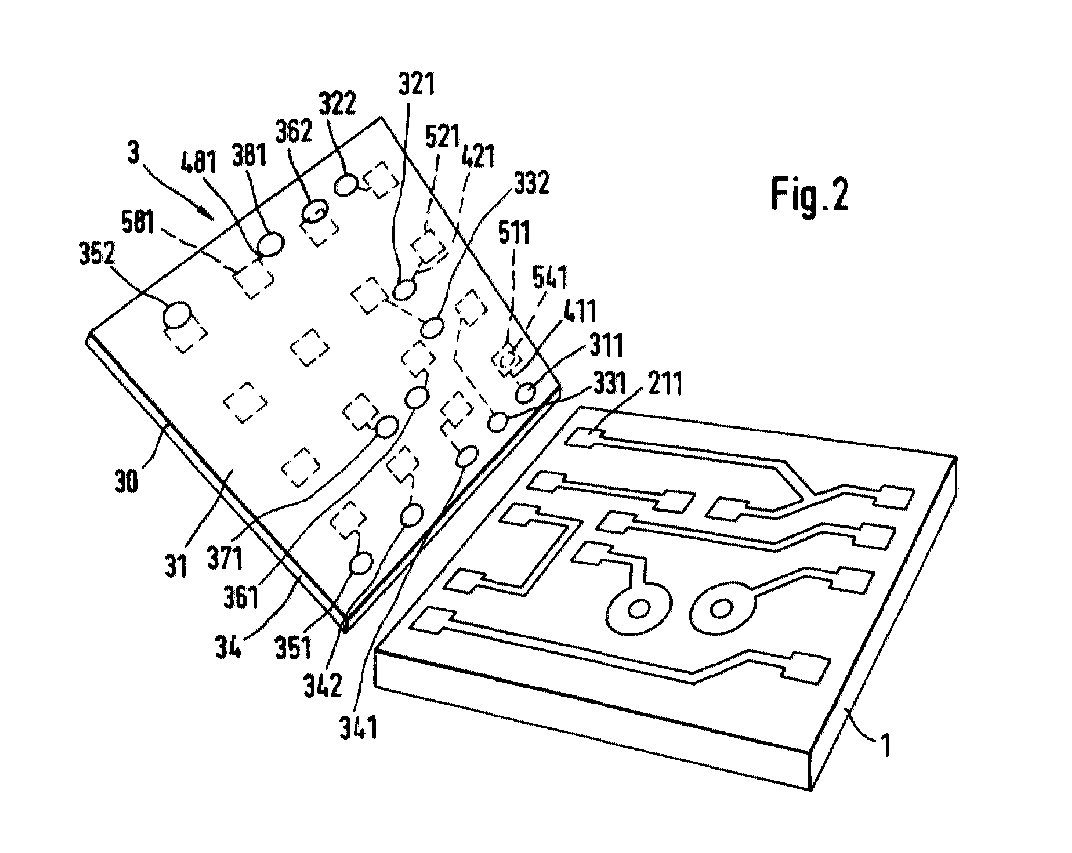
Diese Adapteranordnungen (3, 6) sind zum Testen von auch
großflächigen, Leiterplatten (1) geeignet, deren n
Testpunkte (211 ... 281) nur einen Abstand von etwa 150 µm
haben können. Eine einschichtige flexible Folie (30) aus
Isoliermaterial hat n Kontaktbumps (311 ...381) mit einem
Kontaktierungsteil (3111) und einer Längsachse (3112).
Jeder Kontaktbump führt durch die Folie senkrecht hindurch,
überragt die Vorderseite einstufig und sitzt derart in
einer Bohrung, daß die Längsachse mit deren Mittelachse
zusammenfällt. Während des Testens wird jeder Kontaktbump
mit dem zugehörigen Testpunkt durch flächiges Andrücken der
Folie (30) an die Leiterplatte (1) mechanisch in Berührung
gebracht und dadurch elektrisch kontaktiert. Jeweils ein
Leiterzug (411, 421, 481) verläuft auf der Rückseite der
Folie von einem entsprechenden Kontaktbump zu einem
zugehörigen Kontaktpunkt (511, 521, 581). Jeder
Kontaktpunkt ist mit einer entsprechenden Kontaktnadel
eines Eingangskontaktfelds des Testgeräts mittels dessen
Andrückens an die Rückseite der Folie (30) unter
Zwischenlage einer elektrisch isolierenden, elastisch
federnden Zwischenfolie (34) elektrisch kontaktiert, die
dort, wo eine Kontaktnadel einen Kontaktpunkt zu
kontaktieren hat, eine elektrische Durchkontaktierung
aufweist.

Priority Applications (1)
| Application Number | Priority Date | Filing Date | Title |
|---|---|---|---|
| EP98116790A EP0902297A3 (en) | 1997-09-11 | 1998-09-05 | Adapter devices for testing printed circuit boards |
Applications Claiming Priority (3)
| Application Number | Priority Date | Filing Date | Title |
|---|---|---|---|
| EP97810646 | 1997-09-11 | ||
| EP97810646A EP0902296A1 (en) | 1997-09-11 | 1997-09-11 | Adapter devices for testing printed circuit boards |
| EP98116790A EP0902297A3 (en) | 1997-09-11 | 1998-09-05 | Adapter devices for testing printed circuit boards |
Publications (2)
| Publication Number | Publication Date |
|---|---|
| EP0902297A2 EP0902297A2 (en) | 1999-03-17 |
| EP0902297A3 true EP0902297A3 (en) | 2001-11-28 |
Family
ID=26148060
Family Applications (1)
| Application Number | Title | Priority Date | Filing Date |
|---|---|---|---|
| EP98116790A Withdrawn EP0902297A3 (en) | 1997-09-11 | 1998-09-05 | Adapter devices for testing printed circuit boards |
Country Status (1)
| Country | Link |
|---|---|
| EP (1) | EP0902297A3 (en) |
Families Citing this family (1)
| Publication number | Priority date | Publication date | Assignee | Title |
|---|---|---|---|---|
| US11262398B2 (en) * | 2019-10-31 | 2022-03-01 | Nanya Technology Corporation | Testing fixture and testing assembly |
Citations (4)
| Publication number | Priority date | Publication date | Assignee | Title |
|---|---|---|---|---|
| JPH03237369A (en) * | 1989-12-19 | 1991-10-23 | Nitto Denko Corp | Structure of test head |
| US5228189A (en) * | 1988-11-12 | 1993-07-20 | Mania Gmbh & Co. | Adapter arrangement for electrically connecting flat wire carriers |
| US5252916A (en) * | 1992-01-27 | 1993-10-12 | Everett Charles Technologies, Inc. | Pneumatic test fixture with springless test probes |
| US5399982A (en) * | 1989-11-13 | 1995-03-21 | Mania Gmbh & Co. | Printed circuit board testing device with foil adapter |
-
1998
- 1998-09-05 EP EP98116790A patent/EP0902297A3/en not_active Withdrawn
Patent Citations (4)
| Publication number | Priority date | Publication date | Assignee | Title |
|---|---|---|---|---|
| US5228189A (en) * | 1988-11-12 | 1993-07-20 | Mania Gmbh & Co. | Adapter arrangement for electrically connecting flat wire carriers |
| US5399982A (en) * | 1989-11-13 | 1995-03-21 | Mania Gmbh & Co. | Printed circuit board testing device with foil adapter |
| JPH03237369A (en) * | 1989-12-19 | 1991-10-23 | Nitto Denko Corp | Structure of test head |
| US5252916A (en) * | 1992-01-27 | 1993-10-12 | Everett Charles Technologies, Inc. | Pneumatic test fixture with springless test probes |
Non-Patent Citations (1)
| Title |
|---|
| PATENT ABSTRACTS OF JAPAN vol. 016, no. 019 (P - 1300) 17 January 1992 (1992-01-17) * |
Also Published As
| Publication number | Publication date |
|---|---|
| EP0902297A2 (en) | 1999-03-17 |
Similar Documents
| Publication | Publication Date | Title |
|---|---|---|
| DE10125345B4 (en) | Test contact system with planarization mechanism | |
| DE3812654C2 (en) | ||
| EP0453716B1 (en) | Connector assembly for chip testing | |
| DE202005021386U1 (en) | Probe with a sensor with membrane suspension | |
| DE2344239B2 (en) | CONTACT DEVICE FOR CONNECTING A PRINTED CIRCUIT TO A TESTING DEVICE | |
| US4496903A (en) | Circuit board test fixture | |
| EP0838688A3 (en) | Device and procedure for testing printed circuit boards | |
| DE4324692A1 (en) | Piezoelectric force sensor | |
| EP0838685A3 (en) | Probe card with needle-like probes resiliently supported by rigid substrate and process for fabricating thereof | |
| DE3701310A1 (en) | Contact-making device for making contact with surface-mounted integrated circuits | |
| US5798655A (en) | Contact probe unit including needle members urged by a resilient material block | |
| DE2640613A1 (en) | METHOD AND DEVICE FOR CONTACTING CIRCUIT COMPONENTS IN A LAYERED CIRCUIT | |
| EP0875767A3 (en) | Device and procedure for testing naked circuit boards | |
| DE10043193B4 (en) | Tester for semiconductor substrates | |
| EP1940207A3 (en) | Electric device with a carrier element with a minimum of one special connecting surface and a component mounted on the surface | |
| EP0902297A3 (en) | Adapter devices for testing printed circuit boards | |
| EP0818684A3 (en) | Test system for printed circuits | |
| DE69024292T2 (en) | Interface card for an arrangement to be tested and connections of electronic test cards in semiconductor test systems | |
| DE102004034357A1 (en) | Test cards carrier element | |
| EP0877259A3 (en) | Apparatus for testing an electric circuit board comprising contact points and conductor lines | |
| EP4591071A1 (en) | Method and device for making electrical contact with electronic components | |
| JP2600745Y2 (en) | Jig for integrated circuit inspection equipment | |
| JPS6058831B2 (en) | Characteristic inspection jig for electronic components | |
| EP0406764B1 (en) | Adapter for testing integrated circuits mounted on a film | |
| JPS58155374A (en) | Tester for printed circuit board |
Legal Events
| Date | Code | Title | Description |
|---|---|---|---|
| PUAI | Public reference made under article 153(3) epc to a published international application that has entered the european phase |
Free format text: ORIGINAL CODE: 0009012 |
|
| AK | Designated contracting states |
Kind code of ref document: A2 Designated state(s): AT BE CH CY DE DK ES FI FR GB GR IE IT LI LU MC NL PT SE |
|
| AX | Request for extension of the european patent |
Free format text: AL;LT;LV;MK;RO;SI |
|
| PUAL | Search report despatched |
Free format text: ORIGINAL CODE: 0009013 |
|
| AK | Designated contracting states |
Kind code of ref document: A3 Designated state(s): AT BE CH CY DE DK ES FI FR GB GR IE IT LI LU MC NL PT SE |
|
| AX | Request for extension of the european patent |
Free format text: AL;LT;LV;MK;RO;SI |
|
| AKX | Designation fees paid | ||
| REG | Reference to a national code |
Ref country code: DE Ref legal event code: 8566 |
|
| 19U | Interruption of proceedings before grant |
Effective date: 20020401 |
|
| 19W | Proceedings resumed before grant after interruption of proceedings |
Effective date: 20100401 |
|
| RAP1 | Party data changed (applicant data changed or rights of an application transferred) |
Owner name: WUERTH ELEKTRONIK SCHOPFHEIM GMBH & CO. KG |
|
| STAA | Information on the status of an ep patent application or granted ep patent |
Free format text: STATUS: THE APPLICATION IS DEEMED TO BE WITHDRAWN |
|
| 18D | Application deemed to be withdrawn |
Effective date: 20020529 |