EP0901873A2 - Liquid cristal display for laser marker - Google Patents
Liquid cristal display for laser marker Download PDFInfo
- Publication number
- EP0901873A2 EP0901873A2 EP98120295A EP98120295A EP0901873A2 EP 0901873 A2 EP0901873 A2 EP 0901873A2 EP 98120295 A EP98120295 A EP 98120295A EP 98120295 A EP98120295 A EP 98120295A EP 0901873 A2 EP0901873 A2 EP 0901873A2
- Authority
- EP
- European Patent Office
- Prior art keywords
- liquid crystal
- time
- electrodes
- predetermined
- marking
- Prior art date
- Legal status (The legal status is an assumption and is not a legal conclusion. Google has not performed a legal analysis and makes no representation as to the accuracy of the status listed.)
- Withdrawn
Links
Images


Classifications
-
- B—PERFORMING OPERATIONS; TRANSPORTING
- B23—MACHINE TOOLS; METAL-WORKING NOT OTHERWISE PROVIDED FOR
- B23K—SOLDERING OR UNSOLDERING; WELDING; CLADDING OR PLATING BY SOLDERING OR WELDING; CUTTING BY APPLYING HEAT LOCALLY, e.g. FLAME CUTTING; WORKING BY LASER BEAM
- B23K26/00—Working by laser beam, e.g. welding, cutting or boring
-
- G—PHYSICS
- G06—COMPUTING; CALCULATING OR COUNTING
- G06K—GRAPHICAL DATA READING; PRESENTATION OF DATA; RECORD CARRIERS; HANDLING RECORD CARRIERS
- G06K15/00—Arrangements for producing a permanent visual presentation of the output data, e.g. computer output printers
- G06K15/02—Arrangements for producing a permanent visual presentation of the output data, e.g. computer output printers using printers
- G06K15/12—Arrangements for producing a permanent visual presentation of the output data, e.g. computer output printers using printers by photographic printing, e.g. by laser printers
- G06K15/1238—Arrangements for producing a permanent visual presentation of the output data, e.g. computer output printers using printers by photographic printing, e.g. by laser printers simultaneously exposing more than one point
- G06K15/1257—Arrangements for producing a permanent visual presentation of the output data, e.g. computer output printers using printers by photographic printing, e.g. by laser printers simultaneously exposing more than one point on more than one main scanning line
-
- B—PERFORMING OPERATIONS; TRANSPORTING
- B23—MACHINE TOOLS; METAL-WORKING NOT OTHERWISE PROVIDED FOR
- B23K—SOLDERING OR UNSOLDERING; WELDING; CLADDING OR PLATING BY SOLDERING OR WELDING; CUTTING BY APPLYING HEAT LOCALLY, e.g. FLAME CUTTING; WORKING BY LASER BEAM
- B23K26/00—Working by laser beam, e.g. welding, cutting or boring
- B23K26/02—Positioning or observing the workpiece, e.g. with respect to the point of impact; Aligning, aiming or focusing the laser beam
- B23K26/06—Shaping the laser beam, e.g. by masks or multi-focusing
- B23K26/064—Shaping the laser beam, e.g. by masks or multi-focusing by means of optical elements, e.g. lenses, mirrors or prisms
- B23K26/066—Shaping the laser beam, e.g. by masks or multi-focusing by means of optical elements, e.g. lenses, mirrors or prisms by using masks
-
- G—PHYSICS
- G06—COMPUTING; CALCULATING OR COUNTING
- G06K—GRAPHICAL DATA READING; PRESENTATION OF DATA; RECORD CARRIERS; HANDLING RECORD CARRIERS
- G06K15/00—Arrangements for producing a permanent visual presentation of the output data, e.g. computer output printers
- G06K15/02—Arrangements for producing a permanent visual presentation of the output data, e.g. computer output printers using printers
- G06K15/12—Arrangements for producing a permanent visual presentation of the output data, e.g. computer output printers using printers by photographic printing, e.g. by laser printers
- G06K15/1204—Arrangements for producing a permanent visual presentation of the output data, e.g. computer output printers using printers by photographic printing, e.g. by laser printers involving the fast moving of an optical beam in the main scanning direction
-
- G—PHYSICS
- G06—COMPUTING; CALCULATING OR COUNTING
- G06K—GRAPHICAL DATA READING; PRESENTATION OF DATA; RECORD CARRIERS; HANDLING RECORD CARRIERS
- G06K15/00—Arrangements for producing a permanent visual presentation of the output data, e.g. computer output printers
- G06K15/02—Arrangements for producing a permanent visual presentation of the output data, e.g. computer output printers using printers
- G06K15/12—Arrangements for producing a permanent visual presentation of the output data, e.g. computer output printers using printers by photographic printing, e.g. by laser printers
- G06K15/1238—Arrangements for producing a permanent visual presentation of the output data, e.g. computer output printers using printers by photographic printing, e.g. by laser printers simultaneously exposing more than one point
- G06K15/1242—Arrangements for producing a permanent visual presentation of the output data, e.g. computer output printers using printers by photographic printing, e.g. by laser printers simultaneously exposing more than one point on one main scanning line
- G06K15/1252—Arrangements for producing a permanent visual presentation of the output data, e.g. computer output printers using printers by photographic printing, e.g. by laser printers simultaneously exposing more than one point on one main scanning line using an array of light modulators, e.g. a linear array
Definitions
- the present invention relates to systems for displaying a pattern on a liquid crystal for a laser marker and more particularly, to a system for performing predetermined control over switching of display to attain high speed marking.
- the above display switching operation is not instantaneously carried out and requires a time of about 60 msec. Accordingly, during this display switching time, the liquid crystal is put in its non-display state and the marking is not performed, hence this time period becomes a wasteful time in operation.
- such switching of the display screen is generally continually done and pattern marking operation is often continuously done. In this case, since the above switching time is required whenever the pattern is changed, such switching time is accumulated for each pattern change to reach a lot of loss time when viewed from the entire operation, which hinders realization of high-speed marking.
- An invention for realizing high-speed marking is disclosed, for example, in Japanese Patent Application Laid-Open Publication No. 2-268988, in which the display surface of a liquid crystal mask for a laser marker is divided into 2 upper and lower sections so that, when scanning for the upper half is completed and then scanning starts for the lower half, rewriting is carried out for a marking pattern of the upper half.
- the liquid crystal switching time is roughly divided into a time necessary for extinguishing the pattern being displayed and a time necessary for activating a new display pattern. Between these times, the displayed-pattern extinguishment time, which depends on the composition material, structure, etc. of the liquid crystal mask, cannot be easily shortened.
- a second object of the present invention is to attain high-speed marking while maintaining the marking quality.
- row and column electrodes are provided for each of pixels of a liquid crystal.
- the row and column electrodes are grounded and then predetermined effective voltages (root-mean-square voltages) are applied to the row and column electrodes to perform switching of display of a liquid crystal display screen.
- effective voltages which are larger than the predetermined effective voltages are applied to the electrodes only for a predetermined period of time after starting application of the voltages to the electrodes.
- the predetermined effective voltages are applied to the electrodes after passage of the predetermined period of time.
- the effective voltage to be applied to the liquid crystal is set at a high level only for the predetermined period of time after starting application of the voltage and is set at such a level as to provide a predetermined transmission factor after the passage of the predetermined period of time, a liquid crystal activation response time can be shortened.
- Fig. 1 conceptionally shows an arrangement of a laser marker.
- a laser oscillator 1 oscillates to issue a scanning laser beam (such as a YAG (yttrium aluminum garnet) laser beam), which oscillated laser beam is irradiated on a reflective surface 2a of a deflector 2.
- a scanning laser beam such as a YAG (yttrium aluminum garnet) laser beam
- a laser beam reflected by the reflective surface 2a is illuminated or irradiated on a reflective surface 3a of a deflector 3 made in the form of a polygon mirror through a lens 4.
- the laser beam reflected from the reflective surface 3a is illuminated or irradiated on a liquid crystal display screen 10 of a high polymer compound type liquid crystal mask 6 via a lens 5.
- the reflective surface 2a of the deflector 2 is rotated in a direction shown by an arrow AA by a motor 8, and the reflective surface 3a of the deflector 3 is rotated in a direction shown by an arrow BB by a motor 9. Accordingly, when the drive control of the motor 9 causes rotation of the reflective surface 3a in the arrow BB direction, the laser beam main-scans the liquid crystal display screen 10 of the liquid crystal mask 6 in a direction shown by an arrow X; while, when the drive control of the motor 8 causes rotation of the reflective surface 2a in the arrow AA direction, the laser beam sub-scans the liquid crystal display screen 10 of the liquid crystal mask 6 in a direction shown by an arrow Y. The manner the laser beam scans the liquid crystal display screen 10 is shown by arrows in Fig. 2.
- a controller 7 controls the driving operations of the above motors 8 and 9, controls the laser oscillation of the laser oscillator 1, and outputs a signal for driving the pixels of the liquid crystal display screen 10 of the liquid crystal mask 6.
- the controller 7 on the basis of information on a marking pattern entered through a predetermined input means, outputs a signal for driving associated ones of the pixels of the liquid crystal display screen 10 of the liquid crystal mask 6 corresponding to the pattern. In response to this, the associated pixels on the liquid crystal display screen 10 of the liquid crystal mask 6 are driven. Then the control of the driving operations of the motors 8 and 9 as well as the control of the operation of the laser oscillator 1 cause a laser beam to be scanned so that the laser beam transmits only the driven pixels and passes through a predetermined optical system (not shown), whereby a character, figure, etc. corresponding to a shape (the shape of the marking pattern) of the driven pixels are marked, e.g., on a surface of such a work 13 as shown in Fig. 3.
- a pattern 14 to be marked is divided into a plurality of marking patterns of blocks A to L so that the system of the present embodiment performs sequential marking operation over the respective marking patterns of the blocks. Accordingly, it is necessary to sequentially switch the pixel to be driven on the liquid crystal display screen 10 on a block basis of the blocks A to L.
- the entire liquid crystal display screen is switched at a time.
- the liquid crystal switching time is roughly divided into a time necessary for extinguishing the pattern being displayed and a time necessary for activating a new display pattern. Between these times, the displayed-pattern extinguishing time, which depends on the composition material, structure, etc. of the liquid crystal mask, cannot be easily shortened.
- the effective voltage is defined as the following equation (1).
- Vrms (1/T 0 T V 2 (t)dt) 1/2
- V(t) denotes an applied voltage waveform
- T denotes a period of the applied voltage waveform
- Vrms denotes the effective voltage (root-mean-square voltage).
- the liquid crystal activation response time can be shortened.
- the display activation time can be shortened.
- the conditions so far used can be used as they are while preventing the marking quality from being deteriorated and therefore there can be fabricated a laser marker which has a short marking time.
- such a command is issued from the controller 7 that, as shown in Fig. 5, the effective voltage to be applied from the controller 7 to the mask 6 is set at a high level (V1) for a short time (T1) after starting the display and then reduced to a predetermined level (V2) after passage of the predetermined time (T1) (more concretely, at the timing when the transmission pixels exhibit sufficient transmission factor before the shutter pixels exhibit their transmission property).
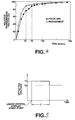
- Fig. 4 shows a response characteristic in a display start mode when such control is carried out. Illustrated data were measured at an environmental temperature of 20°C and the liquid crystal driving voltage V2 was 11 Vrms. Measurement was conducted for comparison between the case where the driving voltage in the liquid crystal display activation mode is 11 Vrms that is the same as the set value V2 and the case where the driving voltage is set to have the voltage V1 of 12.1 Vrms, which is 10% greater than V2, for 40 msec. and thereafter to have the voltage V2 of 11 Vrms.
- an effective voltage to be applied to the liquid crystal is set to be high for a predetermined time after starting the display and reduced to a predetermined level after passage of the predetermined time; display of transmission pixels can be activated with the high effective voltage and the display activation time can be shortened.
- the conditions so far used can be used as they are while preventing the marking quality from being deteriorated and the marking time can be shortened to a large extent.
Abstract
Description
- The present invention relates to systems for displaying a pattern on a liquid crystal for a laser marker and more particularly, to a system for performing predetermined control over switching of display to attain high speed marking.
- For a technique for applying liquid crystal made from so-called high polymer compound to a mask for a laser marker, the applicant of the present application has already filed patent applications (Japanese Patent Application No. 2-268988, etc.).
- In such a high polymer compound type liquid crystal, when it is desired to switch the display screen of the liquid crystal, i.e., a marking pattern, this is attained, for the purpose of preventing from an after-image at the time of the switching of display, by performing such non-display processing that grounds row and column electrodes provided for the respective pixels of the liquid crystal and then by applying predetermined voltages to the row and column electrodes. In this case, ones of the pixels subjected to no application of such voltages are put in their laser-beam scattering state while the other pixels subjected to the application of the voltages are put in their laser-beam transmission state.
- However, the above display switching operation is not instantaneously carried out and requires a time of about 60 msec. Accordingly, during this display switching time, the liquid crystal is put in its non-display state and the marking is not performed, hence this time period becomes a wasteful time in operation. In addition, such switching of the display screen is generally continually done and pattern marking operation is often continuously done. In this case, since the above switching time is required whenever the pattern is changed, such switching time is accumulated for each pattern change to reach a lot of loss time when viewed from the entire operation, which hinders realization of high-speed marking.
- An invention for realizing high-speed marking is disclosed, for example, in Japanese Patent Application Laid-Open Publication No. 2-268988, in which the display surface of a liquid crystal mask for a laser marker is divided into 2 upper and lower sections so that, when scanning for the upper half is completed and then scanning starts for the lower half, rewriting is carried out for a marking pattern of the upper half.
- When analyzed, the liquid crystal switching time is roughly divided into a time necessary for extinguishing the pattern being displayed and a time necessary for activating a new display pattern. Between these times, the displayed-pattern extinguishment time, which depends on the composition material, structure, etc. of the liquid crystal mask, cannot be easily shortened.
- For this reason, for the purpose of realizing high-speed marking, when the marking operation is started before the liquid crystal display appears, irregularities take place in the marking on a workpiece. Accordingly, there has been a limit in realizing higher-speed marking while maintaining the marking quality.
- In view of such circumstances as mentioned above, it is a first object of the present invention to realize high-speed marking for a laser marker with use of, in particular, a high polymer compound type liquid crystal while preventing generation of an after-image.
- A second object of the present invention is to attain high-speed marking while maintaining the marking quality.
- These objects are solved by a liquid crystal display according to claim 1.
- In a liquid crystal display for a laser marker, row and column electrodes are provided for each of pixels of a liquid crystal. The row and column electrodes are grounded and then predetermined effective voltages (root-mean-square voltages) are applied to the row and column electrodes to perform switching of display of a liquid crystal display screen.
- In accordance with the present invention, effective voltages which are larger than the predetermined effective voltages are applied to the electrodes only for a predetermined period of time after starting application of the voltages to the electrodes. The predetermined effective voltages are applied to the electrodes after passage of the predetermined period of time.
- With such an arrangement, since the effective voltage to be applied to the liquid crystal is set at a high level only for the predetermined period of time after starting application of the voltage and is set at such a level as to provide a predetermined transmission factor after the passage of the predetermined period of time, a liquid crystal activation response time can be shortened.
- Fig. 1 shows an arrangement of a liquid crystal display screen switching system for a laser marker in accordance with an embodiment of the present invention;
- Fig. 2 is a diagram for explaining how a laser beam scans a liquid crystal display screen shown in Fig. 1;
- Fig. 3 shows an example for a pattern marked through the system of Fig. 1;
- Fig. 4 is a graph showing a difference in the response characteristic between a liquid crystal in a preferred embodiment of the present invention and a prior art liquid crystal; and
- Fig. 5 is a graph showing a relationship between the time and execution voltage in the preferred embodiment of the present invention.
-
- Fig. 1 conceptionally shows an arrangement of a laser marker.
- In the drawing, a laser oscillator 1 oscillates to issue a scanning laser beam (such as a YAG (yttrium aluminum garnet) laser beam), which oscillated laser beam is irradiated on a
reflective surface 2a of a deflector 2. A laser beam reflected by thereflective surface 2a is illuminated or irradiated on a reflective surface 3a of adeflector 3 made in the form of a polygon mirror through alens 4. The laser beam reflected from the reflective surface 3a is illuminated or irradiated on a liquidcrystal display screen 10 of a high polymer compound typeliquid crystal mask 6 via alens 5. - The
reflective surface 2a of the deflector 2 is rotated in a direction shown by an arrow AA by a motor 8, and the reflective surface 3a of thedeflector 3 is rotated in a direction shown by an arrow BB by a motor 9. Accordingly, when the drive control of the motor 9 causes rotation of the reflective surface 3a in the arrow BB direction, the laser beam main-scans the liquidcrystal display screen 10 of theliquid crystal mask 6 in a direction shown by an arrow X; while, when the drive control of the motor 8 causes rotation of thereflective surface 2a in the arrow AA direction, the laser beam sub-scans the liquidcrystal display screen 10 of theliquid crystal mask 6 in a direction shown by an arrow Y. The manner the laser beam scans the liquidcrystal display screen 10 is shown by arrows in Fig. 2. - A
controller 7 controls the driving operations of the above motors 8 and 9, controls the laser oscillation of the laser oscillator 1, and outputs a signal for driving the pixels of the liquidcrystal display screen 10 of theliquid crystal mask 6. - The
controller 7, on the basis of information on a marking pattern entered through a predetermined input means, outputs a signal for driving associated ones of the pixels of the liquidcrystal display screen 10 of theliquid crystal mask 6 corresponding to the pattern. In response to this, the associated pixels on the liquidcrystal display screen 10 of theliquid crystal mask 6 are driven. Then the control of the driving operations of the motors 8 and 9 as well as the control of the operation of the laser oscillator 1 cause a laser beam to be scanned so that the laser beam transmits only the driven pixels and passes through a predetermined optical system (not shown), whereby a character, figure, etc. corresponding to a shape (the shape of the marking pattern) of the driven pixels are marked, e.g., on a surface of such awork 13 as shown in Fig. 3. - More specifically, as shown in Fig. 3, a
pattern 14 to be marked is divided into a plurality of marking patterns of blocks A to L so that the system of the present embodiment performs sequential marking operation over the respective marking patterns of the blocks. Accordingly, it is necessary to sequentially switch the pixel to be driven on the liquidcrystal display screen 10 on a block basis of the blocks A to L. - In the preferred embodiment, the entire liquid crystal display screen is switched at a time.
- When analyzed, the liquid crystal switching time is roughly divided into a time necessary for extinguishing the pattern being displayed and a time necessary for activating a new display pattern. Between these times, the displayed-pattern extinguishing time, which depends on the composition material, structure, etc. of the liquid crystal mask, cannot be easily shortened.
- Thus, for the purpose of removing the above difficulty, it is necessary to shorten the liquid crystal display activation time. For example, as described in a book entitled "Liquid Crystal Applications", written by Okano and Kobayashi, p85, published by Baifuukan, 1985; transmission factor for liquid crystal is determined by an effective voltage value applied thereto.
- The effective voltage is defined as the following equation (1).
- Hence, when the effective voltage applied to the pixels of the liquid crystal is set at a high level for a short time after display is started while set at such a level as to provide a predetermined transmission factor after passage of a predetermined time, the liquid crystal activation response time can be shortened.
- When it is desired to drive the liquid crystal mask by a multiplex method, since the voltage is applied also to pixels acting as shutters, continuous application of a high effective voltage undesirably results in that the shutter pixels starts exhibiting its transmission property. Since the transmission factor is 0% at the time of starting display and a change in the transmission factor of the shutter pixels requires a time, even application of a high effective voltage will not lead to the fact that the shutters start exhibiting transmission property, whereby the display activation time of the transmission pixels can be made short. And since the effective voltage is decreased to a predetermined level after passage of the predetermined time (more concretely, at the time of exhibiting ), the shutter pixels cannot transmit light therethrough.
- Meanwhile, since display of the transmission pixels is activated with the high effective voltage, the display activation time can be shortened. When the aforementioned invention is applied to a transmission type liquid crystal mask for blocking a laser beam, the conditions so far used can be used as they are while preventing the marking quality from being deteriorated and therefore there can be fabricated a laser marker which has a short marking time.
- More specifically, such a command is issued from the
controller 7 that, as shown in Fig. 5, the effective voltage to be applied from thecontroller 7 to themask 6 is set at a high level (V1) for a short time (T1) after starting the display and then reduced to a predetermined level (V2) after passage of the predetermined time (T1) (more concretely, at the timing when the transmission pixels exhibit sufficient transmission factor before the shutter pixels exhibit their transmission property). - Fig. 4 shows a response characteristic in a display start mode when such control is carried out. Illustrated data were measured at an environmental temperature of 20°C and the liquid crystal driving voltage V2 was 11 Vrms. Measurement was conducted for comparison between the case where the driving voltage in the liquid crystal display activation mode is 11 Vrms that is the same as the set value V2 and the case where the driving voltage is set to have the voltage V1 of 12.1 Vrms, which is 10% greater than V2, for 40 msec. and thereafter to have the voltage V2 of 11 Vrms.
- It will be seen from Fig. 4 that the display activation time is reduced. Our analysis has showed that the time necessary for the transmission factor to change from 0% to 90% is 35 msec. in the case of the application of the present second embodiment, while it is required 70 msec. in the prior art. As a result, even when marking speed was made high, there can be obtained such an effect that no irregularity takes place on the marking surface of a workpiece to be processed.
- In accordance with the present invention, since an effective voltage to be applied to the liquid crystal is set to be high for a predetermined time after starting the display and reduced to a predetermined level after passage of the predetermined time; display of transmission pixels can be activated with the high effective voltage and the display activation time can be shortened. Thus, the conditions so far used can be used as they are while preventing the marking quality from being deteriorated and the marking time can be shortened to a large extent.
Claims (1)
- A liquid crystal display for a laser marker in which row and column electrodes are provided for each of pixels of a liquid crystal, the row and column electrodes are grounded and then predetermined effective voltages are applied to the row and column electrodes to perform switching of display of a liquid crystal display screen,
wherein effective voltages larger than the predetermined effective voltages are applied to the electrodes only for a predetermined period of time after starting application of the voltages to the electrodes and the predetermined effective voltages are applied to the electrodes after passage of the predetermined period of time.
Applications Claiming Priority (7)
| Application Number | Priority Date | Filing Date | Title |
|---|---|---|---|
| JP326073/92 | 1992-11-11 | ||
| JP32607392 | 1992-11-11 | ||
| JP4326073A JP2811138B2 (en) | 1992-11-11 | 1992-11-11 | Laser marking device and laser marking method |
| JP31734392A JP3195449B2 (en) | 1992-11-26 | 1992-11-26 | Liquid crystal display switching device in laser marker |
| JP317343/92 | 1992-11-26 | ||
| JP31734392 | 1992-11-26 | ||
| EP93924802A EP0742071B1 (en) | 1992-11-11 | 1993-11-10 | Liquid crystal display for laser marker |
Related Parent Applications (1)
| Application Number | Title | Priority Date | Filing Date |
|---|---|---|---|
| EP93924802A Division EP0742071B1 (en) | 1992-11-11 | 1993-11-10 | Liquid crystal display for laser marker |
Publications (2)
| Publication Number | Publication Date |
|---|---|
| EP0901873A2 true EP0901873A2 (en) | 1999-03-17 |
| EP0901873A3 EP0901873A3 (en) | 1999-07-28 |
Family
ID=26568994
Family Applications (2)
| Application Number | Title | Priority Date | Filing Date |
|---|---|---|---|
| EP93924802A Expired - Lifetime EP0742071B1 (en) | 1992-11-11 | 1993-11-10 | Liquid crystal display for laser marker |
| EP98120295A Withdrawn EP0901873A3 (en) | 1992-11-11 | 1993-11-10 | Liquid cristal display for laser marker |
Family Applications Before (1)
| Application Number | Title | Priority Date | Filing Date |
|---|---|---|---|
| EP93924802A Expired - Lifetime EP0742071B1 (en) | 1992-11-11 | 1993-11-10 | Liquid crystal display for laser marker |
Country Status (5)
| Country | Link |
|---|---|
| US (1) | US5726673A (en) |
| EP (2) | EP0742071B1 (en) |
| KR (1) | KR950703427A (en) |
| DE (1) | DE69326704T2 (en) |
| WO (1) | WO1994011147A1 (en) |
Families Citing this family (5)
| Publication number | Priority date | Publication date | Assignee | Title |
|---|---|---|---|---|
| JP3263516B2 (en) * | 1994-02-08 | 2002-03-04 | 株式会社小松製作所 | Liquid crystal mask marker image display method |
| JP3265553B2 (en) * | 1994-08-19 | 2002-03-11 | 株式会社小松製作所 | Laser marking method |
| JP2860765B2 (en) * | 1995-03-07 | 1999-02-24 | 株式会社小松製作所 | Control device for laser marking device |
| JPH09277069A (en) * | 1996-04-12 | 1997-10-28 | Komatsu Ltd | Liquid crystal mask, liquid crystal laser marker and marking method using it |
| US20050162380A1 (en) * | 2004-01-28 | 2005-07-28 | Jim Paikattu | Laser sensitive screen |
Citations (1)
| Publication number | Priority date | Publication date | Assignee | Title |
|---|---|---|---|---|
| EP0125692A1 (en) * | 1983-05-16 | 1984-11-21 | Nec Corporation | Laser machining apparatus |
Family Cites Families (7)
| Publication number | Priority date | Publication date | Assignee | Title |
|---|---|---|---|---|
| JPS59121391A (en) * | 1982-12-28 | 1984-07-13 | シチズン時計株式会社 | Liquid crystal display |
| US4778260A (en) * | 1985-04-22 | 1988-10-18 | Canon Kabushiki Kaisha | Method and apparatus for driving optical modulation device |
| JP2633954B2 (en) * | 1989-04-10 | 1997-07-23 | 株式会社日立製作所 | Liquid crystal marking method and device |
| JPH0825044B2 (en) * | 1989-06-15 | 1996-03-13 | 株式会社小松製作所 | Laser printer |
| DE69030537T2 (en) * | 1989-07-20 | 1997-12-04 | Sanyo Electric Co | Liquid crystal projector |
| US5432461A (en) * | 1991-06-28 | 1995-07-11 | Photon Dynamics, Inc. | Method of testing active matrix liquid crystal display substrates |
| US5363117A (en) * | 1991-09-04 | 1994-11-08 | Sony Corporation | Laser-addressed liquid crystal display |
-
1993
- 1993-11-10 WO PCT/JP1993/001637 patent/WO1994011147A1/en active IP Right Grant
- 1993-11-10 DE DE69326704T patent/DE69326704T2/en not_active Expired - Fee Related
- 1993-11-10 EP EP93924802A patent/EP0742071B1/en not_active Expired - Lifetime
- 1993-11-10 EP EP98120295A patent/EP0901873A3/en not_active Withdrawn
- 1993-11-10 US US08/432,186 patent/US5726673A/en not_active Expired - Fee Related
- 1993-11-10 KR KR1019950701444A patent/KR950703427A/en not_active Application Discontinuation
Patent Citations (1)
| Publication number | Priority date | Publication date | Assignee | Title |
|---|---|---|---|---|
| EP0125692A1 (en) * | 1983-05-16 | 1984-11-21 | Nec Corporation | Laser machining apparatus |
Non-Patent Citations (1)
| Title |
|---|
| PATENT ABSTRACTS OF JAPAN vol. 015, no. 025 (M-1071), 21 January 1991 & JP 02 268988 A (HITACHI LTD), 2 November 1990 * |
Also Published As
| Publication number | Publication date |
|---|---|
| EP0742071A4 (en) | 1996-09-19 |
| US5726673A (en) | 1998-03-10 |
| KR950703427A (en) | 1995-09-20 |
| DE69326704D1 (en) | 1999-11-11 |
| EP0901873A3 (en) | 1999-07-28 |
| WO1994011147A1 (en) | 1994-05-26 |
| DE69326704T2 (en) | 2000-06-08 |
| EP0742071B1 (en) | 1999-10-06 |
| EP0742071A1 (en) | 1996-11-13 |
Similar Documents
| Publication | Publication Date | Title |
|---|---|---|
| JP2701183B2 (en) | Liquid crystal mask laser marker | |
| US5198843A (en) | Optical marking system having marking mode selecting function | |
| US5703709A (en) | Method and device for color laser marking | |
| EP0901873A2 (en) | Liquid cristal display for laser marker | |
| EP0872302B1 (en) | Controller of laser marking machine | |
| EP0540346B1 (en) | Electrooptical display apparatus and driver | |
| JP3265553B2 (en) | Laser marking method | |
| US6160603A (en) | Liquid crystal mask, liquid crystal laser marker, and marking method using the same | |
| JP2633954B2 (en) | Liquid crystal marking method and device | |
| JP3673742B2 (en) | Bright spot defect correcting method and apparatus for liquid crystal display device | |
| US5734145A (en) | Laser marking method using laser heated liquid crystal mask | |
| JP2811138B2 (en) | Laser marking device and laser marking method | |
| JP3195449B2 (en) | Liquid crystal display switching device in laser marker | |
| JPH0318491A (en) | Laser printing device | |
| US5760370A (en) | Image display method for liquid crystal mask laser marker | |
| JPH0839283A (en) | Laser beam irradiating device and its method | |
| JPH0732168A (en) | Pulse control printing system and device therefor | |
| JPS61261791A (en) | Projection type screen display unit | |
| JPH03219210A (en) | Liquid crystal display device | |
| JPH07112285A (en) | Laser beam mask marker | |
| JPH07199214A (en) | Display device | |
| JPH06234237A (en) | Laser marking device | |
| KR19990065523A (en) | How to drive a bistable twisted nematic cell |
Legal Events
| Date | Code | Title | Description |
|---|---|---|---|
| PUAI | Public reference made under article 153(3) epc to a published international application that has entered the european phase |
Free format text: ORIGINAL CODE: 0009012 |
|
| 17P | Request for examination filed |
Effective date: 19981027 |
|
| AC | Divisional application: reference to earlier application |
Ref document number: 742071 Country of ref document: EP |
|
| AK | Designated contracting states |
Kind code of ref document: A2 Designated state(s): DE FR GB |
|
| PUAL | Search report despatched |
Free format text: ORIGINAL CODE: 0009013 |
|
| AK | Designated contracting states |
Kind code of ref document: A3 Designated state(s): DE FR GB |
|
| STAA | Information on the status of an ep patent application or granted ep patent |
Free format text: STATUS: THE APPLICATION IS DEEMED TO BE WITHDRAWN |
|
| 18D | Application deemed to be withdrawn |
Effective date: 20000129 |