EP0901149B1 - Source d'électrons à émission d'électrons secondaires pour implanteur d'ions - Google Patents
Source d'électrons à émission d'électrons secondaires pour implanteur d'ions Download PDFInfo
- Publication number
- EP0901149B1 EP0901149B1 EP98307168A EP98307168A EP0901149B1 EP 0901149 B1 EP0901149 B1 EP 0901149B1 EP 98307168 A EP98307168 A EP 98307168A EP 98307168 A EP98307168 A EP 98307168A EP 0901149 B1 EP0901149 B1 EP 0901149B1
- Authority
- EP
- European Patent Office
- Prior art keywords
- target
- chamber
- electron
- electrons
- electron shower
- Prior art date
- Legal status (The legal status is an assumption and is not a legal conclusion. Google has not performed a legal analysis and makes no representation as to the accuracy of the status listed.)
- Expired - Lifetime
Links
- OKTJSMMVPCPJKN-UHFFFAOYSA-N Carbon Chemical compound [C] OKTJSMMVPCPJKN-UHFFFAOYSA-N 0.000 claims description 26
- 229910002804 graphite Inorganic materials 0.000 claims description 26
- 239000010439 graphite Substances 0.000 claims description 26
- 238000010884 ion-beam technique Methods 0.000 claims description 20
- 238000005468 ion implantation Methods 0.000 claims description 7
- 238000011144 upstream manufacturing Methods 0.000 claims description 7
- 239000000463 material Substances 0.000 claims description 6
- 230000003116 impacting effect Effects 0.000 claims description 5
- 229910044991 metal oxide Inorganic materials 0.000 claims 1
- 150000004706 metal oxides Chemical class 0.000 claims 1
- 235000012431 wafers Nutrition 0.000 description 30
- 239000007789 gas Substances 0.000 description 21
- 150000002500 ions Chemical class 0.000 description 19
- 238000000605 extraction Methods 0.000 description 12
- XAGFODPZIPBFFR-UHFFFAOYSA-N aluminium Chemical compound [Al] XAGFODPZIPBFFR-UHFFFAOYSA-N 0.000 description 11
- 229910052782 aluminium Inorganic materials 0.000 description 11
- XKRFYHLGVUSROY-UHFFFAOYSA-N Argon Chemical compound [Ar] XKRFYHLGVUSROY-UHFFFAOYSA-N 0.000 description 6
- 239000011261 inert gas Substances 0.000 description 6
- 238000002347 injection Methods 0.000 description 6
- 239000007924 injection Substances 0.000 description 6
- 230000005684 electric field Effects 0.000 description 5
- 239000011248 coating agent Substances 0.000 description 4
- 238000000576 coating method Methods 0.000 description 4
- XLYOFNOQVPJJNP-UHFFFAOYSA-N water Substances O XLYOFNOQVPJJNP-UHFFFAOYSA-N 0.000 description 4
- 230000002411 adverse Effects 0.000 description 3
- 238000004458 analytical method Methods 0.000 description 3
- 229910052786 argon Inorganic materials 0.000 description 3
- 230000000694 effects Effects 0.000 description 3
- 230000007246 mechanism Effects 0.000 description 3
- 230000003647 oxidation Effects 0.000 description 3
- 238000007254 oxidation reaction Methods 0.000 description 3
- 229910052724 xenon Inorganic materials 0.000 description 3
- FHNFHKCVQCLJFQ-UHFFFAOYSA-N xenon atom Chemical compound [Xe] FHNFHKCVQCLJFQ-UHFFFAOYSA-N 0.000 description 3
- 238000006424 Flood reaction Methods 0.000 description 2
- VYPSYNLAJGMNEJ-UHFFFAOYSA-N Silicium dioxide Chemical compound O=[Si]=O VYPSYNLAJGMNEJ-UHFFFAOYSA-N 0.000 description 2
- 230000001133 acceleration Effects 0.000 description 2
- 230000003247 decreasing effect Effects 0.000 description 2
- 239000002019 doping agent Substances 0.000 description 2
- 239000000284 extract Substances 0.000 description 2
- 239000012530 fluid Substances 0.000 description 2
- 238000002513 implantation Methods 0.000 description 2
- TWNQGVIAIRXVLR-UHFFFAOYSA-N oxo(oxoalumanyloxy)alumane Chemical compound O=[Al]O[Al]=O TWNQGVIAIRXVLR-UHFFFAOYSA-N 0.000 description 2
- 239000004065 semiconductor Substances 0.000 description 2
- XUIMIQQOPSSXEZ-UHFFFAOYSA-N Silicon Chemical compound [Si] XUIMIQQOPSSXEZ-UHFFFAOYSA-N 0.000 description 1
- 238000009825 accumulation Methods 0.000 description 1
- 230000015572 biosynthetic process Effects 0.000 description 1
- 230000005591 charge neutralization Effects 0.000 description 1
- 230000001143 conditioned effect Effects 0.000 description 1
- 230000003750 conditioning effect Effects 0.000 description 1
- 239000004020 conductor Substances 0.000 description 1
- 238000011109 contamination Methods 0.000 description 1
- 239000002826 coolant Substances 0.000 description 1
- 239000000498 cooling water Substances 0.000 description 1
- 230000001627 detrimental effect Effects 0.000 description 1
- 238000010586 diagram Methods 0.000 description 1
- 238000009826 distribution Methods 0.000 description 1
- 238000005516 engineering process Methods 0.000 description 1
- 239000012535 impurity Substances 0.000 description 1
- 239000012212 insulator Substances 0.000 description 1
- 238000011031 large-scale manufacturing process Methods 0.000 description 1
- 238000012423 maintenance Methods 0.000 description 1
- 238000000034 method Methods 0.000 description 1
- 238000012986 modification Methods 0.000 description 1
- 230000004048 modification Effects 0.000 description 1
- 230000010355 oscillation Effects 0.000 description 1
- 229920002120 photoresistant polymer Polymers 0.000 description 1
- 230000008569 process Effects 0.000 description 1
- 230000008707 rearrangement Effects 0.000 description 1
- 238000009419 refurbishment Methods 0.000 description 1
- 239000010703 silicon Substances 0.000 description 1
- 235000012239 silicon dioxide Nutrition 0.000 description 1
- 239000000377 silicon dioxide Substances 0.000 description 1
- 229910052814 silicon oxide Inorganic materials 0.000 description 1
- 239000000243 solution Substances 0.000 description 1
- 238000006467 substitution reaction Methods 0.000 description 1
- 229910052715 tantalum Inorganic materials 0.000 description 1
- GUVRBAGPIYLISA-UHFFFAOYSA-N tantalum atom Chemical compound [Ta] GUVRBAGPIYLISA-UHFFFAOYSA-N 0.000 description 1
- WFKWXMTUELFFGS-UHFFFAOYSA-N tungsten Chemical compound [W] WFKWXMTUELFFGS-UHFFFAOYSA-N 0.000 description 1
- 229910052721 tungsten Inorganic materials 0.000 description 1
- 239000010937 tungsten Substances 0.000 description 1
Images


Classifications
-
- H—ELECTRICITY
- H01—ELECTRIC ELEMENTS
- H01L—SEMICONDUCTOR DEVICES NOT COVERED BY CLASS H10
- H01L21/00—Processes or apparatus adapted for the manufacture or treatment of semiconductor or solid state devices or of parts thereof
- H01L21/02—Manufacture or treatment of semiconductor devices or of parts thereof
- H01L21/04—Manufacture or treatment of semiconductor devices or of parts thereof the devices having potential barriers, e.g. a PN junction, depletion layer or carrier concentration layer
- H01L21/18—Manufacture or treatment of semiconductor devices or of parts thereof the devices having potential barriers, e.g. a PN junction, depletion layer or carrier concentration layer the devices having semiconductor bodies comprising elements of Group IV of the Periodic Table or AIIIBV compounds with or without impurities, e.g. doping materials
- H01L21/26—Bombardment with radiation
-
- H—ELECTRICITY
- H01—ELECTRIC ELEMENTS
- H01J—ELECTRIC DISCHARGE TUBES OR DISCHARGE LAMPS
- H01J37/00—Discharge tubes with provision for introducing objects or material to be exposed to the discharge, e.g. for the purpose of examination or processing thereof
- H01J37/02—Details
- H01J37/026—Means for avoiding or neutralising unwanted electrical charges on tube components
-
- H—ELECTRICITY
- H01—ELECTRIC ELEMENTS
- H01J—ELECTRIC DISCHARGE TUBES OR DISCHARGE LAMPS
- H01J2237/00—Discharge tubes exposing object to beam, e.g. for analysis treatment, etching, imaging
- H01J2237/30—Electron or ion beam tubes for processing objects
- H01J2237/317—Processing objects on a microscale
- H01J2237/31701—Ion implantation
Definitions
- the present invention relates generally to the field of ion implanters, and more specifically to an improved electron shower or flood in an ion implanter.
- a typical ion implanter comprises three sections or subsystems: (i) a terminal for outputting an ion beam, (ii) a beamline for directing and conditioning the beam output by the terminal, and (iii) an end station which contains a semiconductor wafer to be implanted by the conditioned ion beam.
- the terminal includes a source from which a beam of positively charged ions is extracted.
- the beamline components adjust the energy level and focus of the extracted positively charged ion beam on its way toward the wafer to be implanted.
- a problem encountered in the use of such an ion implanter is that of wafer charging. As the positively charged ion beam continues to impact the wafer, the surface of the wafer may accumulate an undesirable excessive positive charge. Resulting electric fields at the wafer surface can damage microcircuitry on the wafer. The problem of accumulated surface charge becomes more pronounced as implanted circuit elements become smaller, because smaller circuit elements are more susceptible to damage caused by the resultant electric fields.
- beam blow-up Another problem encountered in the use of such an ion implanter, especially in low energy applications, is a phenomenon referred to as beam "blow-up", which concerns the tendency for like (positively)-charged ions within the beam to mutually repel each other (also known as the space charge effect). Such mutual repulsion causes a beam of otherwise desired shape to diverge away from an intended beamline path. Beam blow-up is particularly problematic in high current, low energy applications because the high density of ions in the beam (high current) exaggerates the force of mutual repulsion of the ions, and the small velocities (low energy) of the ions allows more time for the repulsive force to act upon the ions before they reach the wafer.
- a known solution to both wafer charging and the beam blow-up phenomenon is the use of an electron or plasma shower.
- Such showers may also be referred to as electron or plasma floods.
- Both electron and plasma showers generate low energy electrons and introduce these electrons into the beam.
- Plasma floods generate a plasma in an arc chamber and the ion beam potential extracts low energy plasma and electrons into the beam.
- Electron showers generate secondary (low energy) electrons which are used to enhance the beam to reduce space charge (beam blow-up) tendencies and wafer charging effects.
- a typical electron shower includes a target chamber in which secondary electrons are generated and an extension tube connected downstream of the target chamber.
- secondary electrons infiltrate and partially neutralize the beam.
- the partially neutralized beam passes through the extension tube toward the wafer to be implanted.
- the trapped low energy electrons thereby neutralize the net charge of the beam which in turn reduces the positive charge accumulation on wafer as the ion beam strikes the wafer surface.
- the neutralized beam is also less likely to experience detrimental beam blow-up characteristics.
- Secondary electrons are generated within the target chamber as follows.
- a filament within the target chamber is electrically heated so that it thermionically emits primary high energy electrons into the chamber. These primary electrons strike the inner surface of the target chamber which emits secondary electrons as a result of the impact.
- the target chamber is typically comprised of aluminum due to its high secondary electron yield.
- an inert gas such as argon or xenon is introduced into the target chamber and ionized, by means of collisions between inert gas molecules and the high energy electrons, to produce an ionized plasma.
- the presence of the ionized plasma enhances generation of secondary electrons by increasing the extraction rate of secondary electrons from the inner surface of the target chamber.
- the high energy primary electrons produced by the filament possess too great an energy to be captured within the ion beam, they do not assist in reducing the tendency of beam blow-up as do the secondary electrons.
- primary electrons which reach the surface of the wafer can adversely negatively charge the wafer surface, possibly to the extent of causing damage to the wafer. It is therefore desirable that the primary electrons emitted by the filament become expended through collisions with either the inert gas molecules or the inner surface of the target chamber.
- US 5,399,871 relates to a plasma flood system for use in ion implantation.
- a plasma and low energy electron generator includes a filament and emits low energy electrons with a negatively biased electron confinement or guide tube having graphite mesh walls.
- the invention provides an electron shower as set out in claim 1. Some preferred details are set out below.
- a plasma-enhanced electron shower for an ion implantation system including a target provided with a chamber at least partially defined by a replaceable graphite liner.
- a filament assembly attached to the target generates and directs a supply of primary electrons toward a surface provided by the graphite liner.
- the graphite liner is biased to a low negative voltage of up to -10 V (approximately - 6V) to insure that secondary electrons emitted therefrom as a result of impacting primary electrons have a uniform low energy.
- the filament assembly includes a filament for thermionically emitting primary electrons; a biased (-300V) filament electrode comprising first and second portions located on either side of the filament and between which the primary electrons are focused; and a grounded extraction aperture for extracting primary electrons from the filament through the filament electrode portions.
- the extracted primary electrons are thereby focused onto the graphite surface, rather than being directed upstream or downstream of the chamber.
- a gas nozzle is attached to the target for introducing into the chamber a supply of gas molecules to be ionized by the primary electrons. The direction of the nozzle is set with respect to the filament assembly to maximize the ionization rate of the gas molecules.
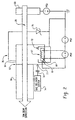
- Figure 1 discloses an ion implanter, generally designated 10, which comprises a terminal 12, a beamline assembly 14 and an end station 16.
- the terminal 12 outputs an ion beam
- the beamline assembly 14 adjusts the focus and energy level of the ion beam and directs it toward a wafer W positioned at the end station 16.
- the terminal 12 includes an ion source 18 having a chamber in which dopant gas from a gas box 20 is injected. Energy is imparted to the ionizable dopant gas to generate positive ions within the source chamber.
- An extraction electrode 22 powered by high voltage supply 24 extracts a beam 26 of positive ions from the source chamber and accelerates the extracted ions toward a mass analysis magnet 28.
- the mass analysis magnet 28 functions to pass only ions of an appropriate charge-to-mass ratio on to the beamline assembly 14. Evacuation of the beam path 29 provided by the mass analysis magnet 28 is provided by vacuum pump 30.
- the beamline assembly 14 comprises a quadrature lens 32, a flag Faraday 34, an electron shower 36, and, optionally, an ion beam acceleration/deceleration electrode (not shown in Figure 1).
- the quadrature lens 32 focuses the ion beam output by the terminal 12 and the flag Faraday 34 measures ion beam characteristics during system set-up.
- the electron shower 36 is further explained below.
- the acceleration/deceleration electrode is used to accelerate or decelerate the focused ion beam to a desired energy level prior to implantation into a wafer at the end station 16. Evacuation of the beam path provided by the beamline assembly 14 is provided by vacuum pump 38.
- the end station 16 includes a disk 40 upon which a plurality of wafers are mounted, a rotary drive mechanism 42 for imparting rotational motion to the disk, and a linear drive mechanism 44 for imparting linear motion to the disk.
- a robotic arm 46 loads wafers onto the disk via a load lock chamber 48. Operation of the system is controlled by an operator control station 50 located at the end of the end station 16.
- FIG. 2 is a schematic of the electron shower 36 which comprises a biased magnetic electron reflector 60 and a target/tube assembly 62.
- the target/tube assembly 62 comprises a target 64 and an extension tube 66, both of which, in the preferred embodiment, are cylindrical in shape.
- the target 64 includes a filament subassembly 67 comprising a filament 68 for thermionically emitting primary electrons, a filament electrode 70 for directing the trajectory of the emitted primary electrons, and an extraction aperture 72.
- a gas delivery system 74 injects a supply of inert gas such as argon or xenon into the interior of the target subassembly 64 by means of valve 76 and gas injection nozzle 77.
- the gas injection nozzle 77 and the filament subassembly 67 are attached to the target 64 at the location of a cutout 78 ( Figure 3).
- the magnetic electron reflector 60 is set to an electrical voltage potential of approximately -2500 volts (V) by a power supply PS1.
- the biased reflector 60 prevents high current ion beams from attracting electrons, thereby preventing beam blow-up.
- the position of the biased reflector away and separate (upstream) from the target/tube assembly 64 ensures that its electric field does not adversely influence primary electron trajectories by urging primary electrons into the extension tube 66 toward the wafer.
- the bias may be eliminated (turned off) to prevent electrons from being stripped from the beam.
- a power supply PS2 of approximately -12V (with respect to the filament electrode 70) supplies the filament 68, and a power supply PS3 of approximately -300V supplies the filament electrode 70.
- the filament is at approximately - 312V with respect to ground potential.
- the extraction aperture 72 is electrically grounded, and a -6V bias voltage is applied to the target 64 by bias (zener) diode 79.
- bias (zener) diode 79 The purposes of these voltage potential differences, the magnitudes of which are made merely for example, is explained further below with respect to Figure 3.
- Figure 3 shows a sectional view of the target/tube assembly 62 of Figure 2.
- the target 64 of the target/tube assembly 62 includes an outer aluminum housing 80 and in inner liner 82 formed of a non-oxidizable (incapable of forming an insulating oxide) material such as graphite and defining a plasma/secondary electron target chamber 84.
- the extension tube 66 of the target/tube assembly also includes an outer aluminum housing 86 and an inner graphite liner 88 attached to the outer housing 86 by means of fasteners such as screws 89.
- the ion beam passes through both the target 64 (arriving through entrance aperture 90 and leaving through exit aperture 92) and the extension tube 66 (arriving through entrance aperture 94 and leaving through exit aperture 96) on its way toward the wafer W to be implanted.
- the target 64 and extension tube 66 are fixedly connected by fasteners such as bolts 98 and collars 99.
- Diode 79 (see Figure 2) applies a bias voltage of -6V to the inner graphite liners 82 and 88 of the target and extension tube, respectively, by means of connecting wire 100.
- the target/tube assembly 62 is attached to a water cooled support 102 which is connected to a mounting plate 104 by means of bolts 106.
- Water inlet 107 permits intake of cooling water to the support 102 (water outlet not shown).
- Insulators 108 electrically isolate the target tube assembly (-6V) from the mounting plate (electrically grounded).
- the mounting plate 104 provides means to install the target/tube assembly into the ion implantation system of Figure 1.
- the filament subassembly 67 generates primary high energy electrons which, upon impact with the inner graphite liner 82 of the target 64, causes emission of secondary lower energy electrons.
- the high energy electrons also indirectly enhance the secondary electron emission rate by ionizing gas which is injected into the chamber 84 by gas injection nozzle 77. Ionization of the gas molecules creates a plasma which increases the secondary electron emission rate of the inner graphite liner 82.
- the filament assembly 67 is shown in greater detail in Figure 4.
- the filament 68 is comprised of a plurality of tungsten segments connected end-to-end and supported by tantalum legs 106 which are fixedly attached to an electrically insulating block 108 by fasteners 110.
- the filament electrode 70 is attached to the insulating block 108 by fasteners 112, and the extraction aperture 72 is attached to the insulating block by fasteners 114.
- Power is provided from PS2 ( Figure 2) to the filament 68 through connectors 112 and 114.
- the negative terminal of PS2 (connector 114) is also connected to the filament electrode 70 by means of conductor 116 and fastener 112.
- Extraction aperture 72 which is constructed from graphite, remains at electrical ground potential.
- the filament 68 emits primary electrons, by means of thermionic emission, which are drawn into the chamber 84 ( Figure 3) by grounded aperture 72. These high energy electrons impact an inner surface 118 of the inner graphite liner 82 of the target 64. Upon impact, the surface 118 of the graphite liner emits secondary electrons having energies much less than the impacting primary electrons. For example, the primary electrons assume energies of up to 312 electron-Volts (eV) when passing through the electrical field provided by the filament electrode (-312V), while most of the emitted secondary electrons only possess energies of less than 20eV.
- eV electron-Volts
- the filament assembly 67 of Figure 4 provides a focusing mechanism for directing the primary electrons thermionically emitted by the filament 68.
- the end-to-end length of the filament (2-3 inches) provides sufficient surface area to create an adequate supply of primary electrons.
- the negatively biased filament electrode 70 comprises portions 70A and 70B which surround the filament 68 and ensure that the filament only experience an electric field in the direction of the extraction aperture 72. Thus, the filament electrode 70 tends to focus the primary electrons toward the center of the electrode so that they are drawn into the chamber 84 through the center of the grounded extraction aperture 72.
- the primary electrons are focused directly at the inner surface 118 of the graphite liner 82 of the chamber 84, and not downstream toward the wafer (through chamber exit aperture 92) or upstream toward the terminal 12 (through chamber entrance aperture 90).
- more primary electrons are directed to the graphite inner surface 118, improving the efficiency of secondary electron generation, and minimizing the adverse effects of primary electrons drifting upstream or downstream of the chamber 84.
- the present embodiment also provides for more uniformity in the energy levels of the generated secondary electrons.
- the use of graphite as a replaceable inner liner of the chamber 84 prevents oxidation of the inner surface 118, which would otherwise occur if the inner surface were constructed from aluminum.
- the energy level of secondary electrons emitted by the graphite surface 118 as a result of the impacting primary high energy electrons does not drift upward due to uncontrolled formation of an oxide coating on the surface.
- the secondary electrons which are emitted from the surface 118 generally assume an energy level consistent with the bias applied to the graphite inner liner, within a secondary electron normal distribution, resulting in better control of the energy levels of the secondary electrons.
- These low energy electrons become thermalized in the plasma created within chamber 84 and are easily captured by the beam potential. The low energy electrons have a low amplitude of oscillation and spend most of their time within the ion beam core.
- Plasma is created in the chamber 84 to increase the secondary electron emission rate by extracting secondary electrons from the surface 118.
- the plasma is created by an inert gas, such as argon or xenon, which is injected into the chamber 84 via the nozzle 77 of Figures 5 and 6 (see also Figures 2 and 3), and ionized by impact with the high energy electrons emitted from filament 68.
- the plasma surrounds the ion beam, creating a sheath between the plasma and the inner surface 118 of the chamber 84 (see Figure 8).
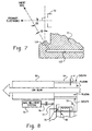
- the nozzle 77 is comprised of aluminum and is attached to the target 64 at the location of cutout 78 ( Figure 3) by means of fasteners installed through holes 119. Curved surface 120 mates with the cylindrical target 64.
- the nozzle includes a fluid inlet 121 and a fluid outlet 122 through which water may be provided and drained, respectively, to provide a cooling medium during operation thereof.
- the gas is provided through passageway 123 and injected into the chamber 84 through inlet 124.
- the inlet 124 has an aspect (length-to-diameter) ratio of greater than 5:1 (approximately 10:1 in the preferred embodiment) and is directed toward the stream of primary electrons which are emitted from the filament 68. As shown in Figure 7, the inlet (124) is pointed slightly forward, at an angle ⁇ of approximately 10 and 30 degrees (preferably 15 to 25 degrees), beyond the grounded extraction aperture 72. Accordingly, the streams of primary electrons and gas molecules are emitted in directions which meet at an angle a of about 60 to 80 degrees (preferably 65 to 75 degrees).
- Such an orientation of the gas inlet (124) with respect to the primary electron extraction aperture (72) insures that the gas molecule stream, which begins to diverge (at approximately 10 degrees) as it exits the inlet 124, maximally intersects the primary electron stream, which is also diverging as it exits aperture 72. Accordingly, the ionization rate of the gas molecules is increased, resulting in an increased plasma density and corresponding increase in secondary electron emission rate.
- the secondary emission rate is also enhanced by the cylindrical surface area of inner surface 118 which is significantly larger than would be provided if the surface 118 were located at the radial location of apertures 90 and 92, instead of radially beyond ( Figure 3). Because the radius of the apertures 90 and 92 is substantially less than the radius of the cylindrical chamber 84, the ends of the cylindrical chamber 84 remain partially closed, serving to maintain plasma pressure (and thus density) as well as prevent the plasma from being conducted upstream. Exit aperture 92 also prevents sputtered material from the wafer W and disk 40 from contaminating the interior of the chamber.
- the increased volume and density of the plasma within the chamber 84 results in a corresponding decreased distance d between the plasma and the inner surface 118 of the chamber ( Figure 8), because a plasma of higher density requires a smaller sheath to shield a given potential.
- the secondary electron emission rate increases with decreasing distance d, per the Child-Langmuir law.
- the secondary electron emission rate also increases with increased plasma density and volume, because increased ionization results in that the primary electrons have a greater chance for collision with a gas molecule.
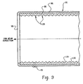
- Figure 9 shows in greater detail the extension tube 66, which is comprised of cylindrical aluminum housing 86 and cylindrical inner liner 88 formed of a non-oxidizable material such as graphite.
- the extension tube 66 shunts the primary high energy electrons generated within the target 64 and prevents these electrons from reaching the surface of the wafer. In this manner, the extension tube 66 prevents an undesirable negative charge from accumulating on the surface of the wafer.
- the inner graphite liner is provided with serrations 126.
- the serrations 126 are formed by alternating adjacent wafer-facing surfaces 128 and target-facing surfaces 130, which face in first and second directions, respectively.
- Photoresist or other material such as silicon or silicon dioxide
- the wafer-facing surfaces become electrically non-conductive.
- the target-facing surfaces remain clean and therefore conductive.
- the conductive target-facing surfaces provide a shunt (low resistance) path to ground for high energy electrons generated in the electron shower.
- the terms "serrated” and “serrations” are used to broadly describe a surface having both wafer-facing surfaces and target-facing surfaces, e.g. , a notched, undulating, or stepped surface.
- the tube is connected to the target 64, it is also biased to -6V by the zener diode 79. Biasing the extension tube 66 at a low negative potential prevents low energy secondary electrons generated by the electron shower from being shunted away from the wafer and keeps them available for wafer charge neutralization, even when the electron shower is first used. The biased tube therefore does not require a period of time before operation stabilizes, as would be required if the tube were not biased.
- the present invention also provides a plasma-enhanced electron shower which is easily refurbished over the course of its useable lifetime.
- the target 64 and the extension tube 66 of the target/tube assembly 62 are both provided with inner graphite liners, 82 and 88, respectively, which may are easily replaced during maintenance operations.
- extension tube 66 may be detached from target 64 by removing bolts 98 and collars 99.
- Filament assembly 67 may be removed from its position within the cutout 78 of target 64.
- the inner liner 82 may be slid out of the aluminum housing 80 in the direction of exit aperture 92. A new liner may then be installed into the aluminum housing 80.
- the inner liner 89 may be slid out of the aluminum housing 86 in the direction of the entrance aperture 94. A new inner liner 89 may then be installed into the aluminum housing 86 and secured into position with screws 89.
- the re-lined extension tube 66 may then be reattached to the re-lined target 64, by means of bolts 98 and collars 99, to complete the target/tube assembly refurbishment process.
Landscapes
- Engineering & Computer Science (AREA)
- Analytical Chemistry (AREA)
- Physics & Mathematics (AREA)
- Chemical & Material Sciences (AREA)
- Health & Medical Sciences (AREA)
- Toxicology (AREA)
- High Energy & Nuclear Physics (AREA)
- Condensed Matter Physics & Semiconductors (AREA)
- General Physics & Mathematics (AREA)
- Manufacturing & Machinery (AREA)
- Computer Hardware Design (AREA)
- Microelectronics & Electronic Packaging (AREA)
- Power Engineering (AREA)
- Physical Vapour Deposition (AREA)
- Electron Sources, Ion Sources (AREA)
Claims (8)
- Dispositif à gerbe d'électrons (62) pour un système d'implantation ionique (10) comportant :caractérisée en ce que :(i) une cible (64) ayant une chambre (84) avec une ouverture d'entrée (90) et une ouverture de sortie (92) à travers lesquelles un faisceau ionique peut passer depuis l'amont de ladite cible vers l'aval de ladite cible,(ii) un ensemble de filament (67) pour générer une alimentation d'électrons primaires à haute énergie et conçu pour diriger lesdits électrons primaires en direction d'une surface (118) de ladite chambre (84) pour provoquer l'émission d'électrons secondaires d'énergie inférieure, et(iii) une source de tension (79) pour générer en tension à appliquer à ladite surface de chambre (118) afin d'établir une polarisation électrique pour celle-ci,ladite surface de chambre est une surface en graphite, munie d'un revêtement intérieur en graphite remplaçable (82).
- Dispositif à gerbe d'électrons (62) selon la revendication 1, dans laquelle ladite chambre (84) a une forme généralement cylindrique, et lesdites ouvertures d'entrée et de sortie (90, 92) sont formées sous forme d'ouvertures partielles dans des extrémités fermées respectives de ladite chambre cylindrique.
- Dispositif à gerbe d'électrons (62) selon la revendication 1, comportant de plus un réflecteur d'électrons (60) positionné en amont de ladite cible (64).
- Dispositif à gerbe d'électrons (62) selon la revendication 3, dans laquelle ledit réflecteur d'électrons (60) est polarisé à une tension négative par une première alimentation en énergie (PS1).
- Dispositif à gerbe d'électrons (62) selon la revendication 1, comportant de plus un tube de prolongement (66) connecté à ladite cible (64) en aval de ladite cible, ledit tube de prolongement (66) comportant une surface intérieure comprenant un matériau ne formant pas un oxyde métallique qui est polarisé électriquement à une tension prédéterminée.
- Dispositif à gerbe d'électrons (62) selon la revendication 5, dans laquelle ladite surface intérieure est constituée d'un revêtement intérieur en graphite remplaçable (88).
- Dispositif à gerbe d'électrons (62) selon la revendication 1, dans laquelle ladite tension appliquée à ladite surface en graphite (118) est suffisamment faible pour amener des électrons secondaires émis depuis celle-ci résultant d'un impact par lesdits électrons primaires, à avoir des énergies essentiellement inférieures à celles desdits électrons primaires d'impact.
- Dispositif à gerbe d'électrons (62) selon la revendication 7, dans laquelle ladite tension appliquée à ladite surface en graphite (118) est fournie par l'intermédiaire d'une diode de polarisation.
Applications Claiming Priority (2)
| Application Number | Priority Date | Filing Date | Title |
|---|---|---|---|
| US924969 | 1997-09-08 | ||
| US08/924,969 US5909031A (en) | 1997-09-08 | 1997-09-08 | Ion implanter electron shower having enhanced secondary electron emission |
Publications (3)
| Publication Number | Publication Date |
|---|---|
| EP0901149A2 EP0901149A2 (fr) | 1999-03-10 |
| EP0901149A3 EP0901149A3 (fr) | 2000-10-18 |
| EP0901149B1 true EP0901149B1 (fr) | 2005-01-05 |
Family
ID=25451002
Family Applications (1)
| Application Number | Title | Priority Date | Filing Date |
|---|---|---|---|
| EP98307168A Expired - Lifetime EP0901149B1 (fr) | 1997-09-08 | 1998-09-04 | Source d'électrons à émission d'électrons secondaires pour implanteur d'ions |
Country Status (6)
| Country | Link |
|---|---|
| US (1) | US5909031A (fr) |
| EP (1) | EP0901149B1 (fr) |
| JP (1) | JP4470126B2 (fr) |
| KR (1) | KR100386875B1 (fr) |
| DE (1) | DE69828469T2 (fr) |
| TW (1) | TW399239B (fr) |
Families Citing this family (12)
| Publication number | Priority date | Publication date | Assignee | Title |
|---|---|---|---|---|
| EP1080482B1 (fr) * | 1998-05-22 | 2002-10-16 | Varian Semiconductor Equipment Associates Inc. | Procede et dispositif d'implantation d'ions de faible energie |
| US6541780B1 (en) * | 1998-07-28 | 2003-04-01 | Varian Semiconductor Equipment Associates, Inc. | Particle beam current monitoring technique |
| JP2000133197A (ja) * | 1998-10-30 | 2000-05-12 | Applied Materials Inc | イオン注入装置 |
| US7378670B2 (en) * | 2001-06-22 | 2008-05-27 | Toyo Tanso Co., Ltd. | Shielding assembly for a semiconductor manufacturing apparatus and method of using the same |
| JP2005527965A (ja) * | 2001-08-28 | 2005-09-15 | ハイニックス セミコンダクター マニュファクチュアリング アメリカ インコーポレイテッド | プラズマチャンバ用チャンバシールド |
| KR100546336B1 (ko) * | 2003-07-03 | 2006-01-26 | 삼성전자주식회사 | 복수의 교점을 가지는 오버레이 키 및 이를 이용한오버레이 측정 방법 |
| KR100598102B1 (ko) * | 2004-05-12 | 2006-07-07 | 삼성전자주식회사 | 이온 주입 설비에 사용되는 이온 발생 장치 |
| US7358508B2 (en) * | 2005-11-10 | 2008-04-15 | Axcelis Technologies, Inc. | Ion implanter with contaminant collecting surface |
| GB2440414B (en) * | 2006-07-12 | 2010-10-27 | Applied Materials Inc | An ion beam guide tube |
| US7629597B2 (en) * | 2006-08-18 | 2009-12-08 | Axcelis Technologies, Inc. | Deposition reduction system for an ion implanter |
| US8330127B2 (en) * | 2008-03-31 | 2012-12-11 | Varian Semiconductor Equipment Associates, Inc. | Flexible ion source |
| CN105097460A (zh) * | 2014-05-09 | 2015-11-25 | 中芯国际集成电路制造(上海)有限公司 | 一种解决离子注入机路径污染的方法 |
Family Cites Families (12)
| Publication number | Priority date | Publication date | Assignee | Title |
|---|---|---|---|---|
| JPS6410563A (en) * | 1987-07-02 | 1989-01-13 | Sumitomo Eaton Nova | Electric charging suppressor of ion implanter |
| US4804837A (en) * | 1988-01-11 | 1989-02-14 | Eaton Corporation | Ion implantation surface charge control method and apparatus |
| JP2805795B2 (ja) * | 1989-02-13 | 1998-09-30 | 富士通株式会社 | イオンビーム照射装置 |
| JPH07120516B2 (ja) * | 1990-07-26 | 1995-12-20 | 株式会社東芝 | 低エネルギ−電子の照射方法および照射装置 |
| US5134299A (en) * | 1991-03-13 | 1992-07-28 | Eaton Corporation | Ion beam implantation method and apparatus for particulate control |
| US5164599A (en) * | 1991-07-19 | 1992-11-17 | Eaton Corporation | Ion beam neutralization means generating diffuse secondary emission electron shower |
| US5466929A (en) * | 1992-02-21 | 1995-11-14 | Hitachi, Ltd. | Apparatus and method for suppressing electrification of sample in charged beam irradiation apparatus |
| US5343047A (en) * | 1992-06-27 | 1994-08-30 | Tokyo Electron Limited | Ion implantation system |
| JP3054302B2 (ja) * | 1992-12-02 | 2000-06-19 | アプライド マテリアルズ インコーポレイテッド | イオン注入中の半導体ウェハにおける帯電を低減するプラズマ放出システム |
| JPH06216060A (ja) * | 1993-01-12 | 1994-08-05 | Tokyo Electron Ltd | 真空処理方法 |
| US5531420A (en) * | 1994-07-01 | 1996-07-02 | Eaton Corporation | Ion beam electron neutralizer |
| US5656092A (en) * | 1995-12-18 | 1997-08-12 | Eaton Corporation | Apparatus for capturing and removing contaminant particles from an interior region of an ion implanter |
-
1997
- 1997-09-08 US US08/924,969 patent/US5909031A/en not_active Expired - Lifetime
-
1998
- 1998-08-19 TW TW087113626A patent/TW399239B/zh not_active IP Right Cessation
- 1998-09-04 DE DE69828469T patent/DE69828469T2/de not_active Expired - Lifetime
- 1998-09-04 EP EP98307168A patent/EP0901149B1/fr not_active Expired - Lifetime
- 1998-09-07 KR KR10-1998-0036755A patent/KR100386875B1/ko not_active IP Right Cessation
- 1998-09-08 JP JP25367798A patent/JP4470126B2/ja not_active Expired - Lifetime
Also Published As
| Publication number | Publication date |
|---|---|
| DE69828469D1 (de) | 2005-02-10 |
| EP0901149A2 (fr) | 1999-03-10 |
| JPH11154484A (ja) | 1999-06-08 |
| US5909031A (en) | 1999-06-01 |
| EP0901149A3 (fr) | 2000-10-18 |
| KR19990029595A (ko) | 1999-04-26 |
| KR100386875B1 (ko) | 2003-08-21 |
| JP4470126B2 (ja) | 2010-06-02 |
| TW399239B (en) | 2000-07-21 |
| DE69828469T2 (de) | 2006-05-18 |
Similar Documents
| Publication | Publication Date | Title |
|---|---|---|
| JP4117507B2 (ja) | イオン注入装置、その内側表面からの汚染物質の除去方法とそのための除去装置 | |
| CA2181076C (fr) | Methode et appareil d'extraction in situ de contaminants provenant d'appareil de neutralisation et d'implantation a faisceaux ioniques | |
| KR100354992B1 (ko) | 이온빔중화방법및장치 | |
| US5903009A (en) | Biased and serrated extension tube for ion implanter electron shower | |
| US5399871A (en) | Plasma flood system for the reduction of charging of wafers during ion implantation | |
| KR101464484B1 (ko) | 이온 비임 임플란터를 위한 플라즈마 전자 플러드 | |
| EP0901149B1 (fr) | Source d'électrons à émission d'électrons secondaires pour implanteur d'ions | |
| KR0152449B1 (ko) | 확산이차 방출전자샤워 | |
| KR100904313B1 (ko) | 이온 빔에 대한 오염 입자 제거 시스템 및 방법 | |
| KR19990078443A (ko) | 이온주입장치 및 방법, 이온 빔 소오스와 가변 슬릿 기구 | |
| JP3758520B2 (ja) | イオンビーム照射装置および関連の方法 | |
| US6501081B1 (en) | Electron flood apparatus for neutralizing charge build up on a substrate during ion implantation | |
| US6359286B1 (en) | Method and apparatus for neutralizing space charge in an ion beam | |
| EP0995214B1 (fr) | Procede et appareil de neutralisation de la charge d'espace dans un faisceau d'ions |
Legal Events
| Date | Code | Title | Description |
|---|---|---|---|
| PUAI | Public reference made under article 153(3) epc to a published international application that has entered the european phase |
Free format text: ORIGINAL CODE: 0009012 |
|
| AK | Designated contracting states |
Kind code of ref document: A2 Designated state(s): DE FR GB IT NL |
|
| AX | Request for extension of the european patent |
Free format text: AL;LT;LV;MK;RO;SI |
|
| 17P | Request for examination filed |
Effective date: 20000502 |
|
| RAP1 | Party data changed (applicant data changed or rights of an application transferred) |
Owner name: AXCELIS TECHNOLOGIES, INC. |
|
| PUAL | Search report despatched |
Free format text: ORIGINAL CODE: 0009013 |
|
| AK | Designated contracting states |
Kind code of ref document: A3 Designated state(s): AT BE CH CY DE DK ES FI FR GB GR IE IT LI LU MC NL PT SE |
|
| AX | Request for extension of the european patent |
Free format text: AL;LT;LV;MK;RO;SI |
|
| AKX | Designation fees paid |
Free format text: DE FR GB IT NL |
|
| 17Q | First examination report despatched |
Effective date: 20030225 |
|
| GRAP | Despatch of communication of intention to grant a patent |
Free format text: ORIGINAL CODE: EPIDOSNIGR1 |
|
| GRAS | Grant fee paid |
Free format text: ORIGINAL CODE: EPIDOSNIGR3 |
|
| GRAA | (expected) grant |
Free format text: ORIGINAL CODE: 0009210 |
|
| AK | Designated contracting states |
Kind code of ref document: B1 Designated state(s): DE FR GB IT NL |
|
| REG | Reference to a national code |
Ref country code: GB Ref legal event code: FG4D |
|
| REF | Corresponds to: |
Ref document number: 69828469 Country of ref document: DE Date of ref document: 20050210 Kind code of ref document: P |
|
| PLBE | No opposition filed within time limit |
Free format text: ORIGINAL CODE: 0009261 |
|
| STAA | Information on the status of an ep patent application or granted ep patent |
Free format text: STATUS: NO OPPOSITION FILED WITHIN TIME LIMIT |
|
| ET | Fr: translation filed | ||
| 26N | No opposition filed |
Effective date: 20051006 |
|
| REG | Reference to a national code |
Ref country code: GB Ref legal event code: FG4D |
|
| PGFP | Annual fee paid to national office [announced via postgrant information from national office to epo] |
Ref country code: NL Payment date: 20070806 Year of fee payment: 10 |
|
| PGFP | Annual fee paid to national office [announced via postgrant information from national office to epo] |
Ref country code: GB Payment date: 20080808 Year of fee payment: 11 |
|
| PG25 | Lapsed in a contracting state [announced via postgrant information from national office to epo] |
Ref country code: NL Free format text: LAPSE BECAUSE OF NON-PAYMENT OF DUE FEES Effective date: 20090401 |
|
| NLV4 | Nl: lapsed or anulled due to non-payment of the annual fee |
Effective date: 20090401 |
|
| GBPC | Gb: european patent ceased through non-payment of renewal fee |
Effective date: 20090904 |
|
| PG25 | Lapsed in a contracting state [announced via postgrant information from national office to epo] |
Ref country code: GB Free format text: LAPSE BECAUSE OF NON-PAYMENT OF DUE FEES Effective date: 20090904 |
|
| PGFP | Annual fee paid to national office [announced via postgrant information from national office to epo] |
Ref country code: DE Payment date: 20100930 Year of fee payment: 13 |
|
| PGFP | Annual fee paid to national office [announced via postgrant information from national office to epo] |
Ref country code: FR Payment date: 20110901 Year of fee payment: 14 |
|
| PGFP | Annual fee paid to national office [announced via postgrant information from national office to epo] |
Ref country code: IT Payment date: 20110922 Year of fee payment: 14 |
|
| REG | Reference to a national code |
Ref country code: FR Ref legal event code: ST Effective date: 20130531 |
|
| PG25 | Lapsed in a contracting state [announced via postgrant information from national office to epo] |
Ref country code: DE Free format text: LAPSE BECAUSE OF NON-PAYMENT OF DUE FEES Effective date: 20130403 |
|
| PG25 | Lapsed in a contracting state [announced via postgrant information from national office to epo] |
Ref country code: IT Free format text: LAPSE BECAUSE OF NON-PAYMENT OF DUE FEES Effective date: 20120904 Ref country code: FR Free format text: LAPSE BECAUSE OF NON-PAYMENT OF DUE FEES Effective date: 20121001 |
|
| REG | Reference to a national code |
Ref country code: DE Ref legal event code: R119 Ref document number: 69828469 Country of ref document: DE Effective date: 20130403 |