EP0897219A2 - Schaltungsanordnung zur Verlustleistungsentlastung von Leistungshalbleiterschaltern in Gleichstromstellern - Google Patents
Schaltungsanordnung zur Verlustleistungsentlastung von Leistungshalbleiterschaltern in Gleichstromstellern Download PDFInfo
- Publication number
- EP0897219A2 EP0897219A2 EP98250202A EP98250202A EP0897219A2 EP 0897219 A2 EP0897219 A2 EP 0897219A2 EP 98250202 A EP98250202 A EP 98250202A EP 98250202 A EP98250202 A EP 98250202A EP 0897219 A2 EP0897219 A2 EP 0897219A2
- Authority
- EP
- European Patent Office
- Prior art keywords
- wiring
- diode
- anode
- power semiconductor
- circuit arrangement
- Prior art date
- Legal status (The legal status is an assumption and is not a legal conclusion. Google has not performed a legal analysis and makes no representation as to the accuracy of the status listed.)
- Granted
Links
Images



Classifications
-
- H—ELECTRICITY
- H03—ELECTRONIC CIRCUITRY
- H03K—PULSE TECHNIQUE
- H03K17/00—Electronic switching or gating, i.e. not by contact-making and –breaking
- H03K17/08—Modifications for protecting switching circuit against overcurrent or overvoltage
- H03K17/081—Modifications for protecting switching circuit against overcurrent or overvoltage without feedback from the output circuit to the control circuit
- H03K17/0814—Modifications for protecting switching circuit against overcurrent or overvoltage without feedback from the output circuit to the control circuit by measures taken in the output circuit
- H03K17/08142—Modifications for protecting switching circuit against overcurrent or overvoltage without feedback from the output circuit to the control circuit by measures taken in the output circuit in field-effect transistor switches
-
- H—ELECTRICITY
- H03—ELECTRONIC CIRCUITRY
- H03K—PULSE TECHNIQUE
- H03K17/00—Electronic switching or gating, i.e. not by contact-making and –breaking
- H03K17/08—Modifications for protecting switching circuit against overcurrent or overvoltage
- H03K17/081—Modifications for protecting switching circuit against overcurrent or overvoltage without feedback from the output circuit to the control circuit
- H03K17/0814—Modifications for protecting switching circuit against overcurrent or overvoltage without feedback from the output circuit to the control circuit by measures taken in the output circuit
- H03K17/08144—Modifications for protecting switching circuit against overcurrent or overvoltage without feedback from the output circuit to the control circuit by measures taken in the output circuit in thyristor switches
-
- H—ELECTRICITY
- H03—ELECTRONIC CIRCUITRY
- H03K—PULSE TECHNIQUE
- H03K17/00—Electronic switching or gating, i.e. not by contact-making and –breaking
- H03K17/08—Modifications for protecting switching circuit against overcurrent or overvoltage
- H03K17/081—Modifications for protecting switching circuit against overcurrent or overvoltage without feedback from the output circuit to the control circuit
- H03K17/0814—Modifications for protecting switching circuit against overcurrent or overvoltage without feedback from the output circuit to the control circuit by measures taken in the output circuit
- H03K17/08146—Modifications for protecting switching circuit against overcurrent or overvoltage without feedback from the output circuit to the control circuit by measures taken in the output circuit in bipolar transistor switches
-
- H—ELECTRICITY
- H03—ELECTRONIC CIRCUITRY
- H03K—PULSE TECHNIQUE
- H03K17/00—Electronic switching or gating, i.e. not by contact-making and –breaking
- H03K17/08—Modifications for protecting switching circuit against overcurrent or overvoltage
- H03K17/081—Modifications for protecting switching circuit against overcurrent or overvoltage without feedback from the output circuit to the control circuit
- H03K17/0814—Modifications for protecting switching circuit against overcurrent or overvoltage without feedback from the output circuit to the control circuit by measures taken in the output circuit
- H03K17/08148—Modifications for protecting switching circuit against overcurrent or overvoltage without feedback from the output circuit to the control circuit by measures taken in the output circuit in composite switches
Definitions
- the invention relates to a circuit arrangement for power loss relief a power semiconductor switch, the one in series with a load in the branch of a DC voltage source lies, with an anti-parallel to the load Free-wheeling diode is arranged, in particular for direct current controllers.
- the energy of both circuit chokes initially cached in a storage capacitor and then fed back into the load. After an expanded for the purpose of shutdown relief Execution is initially in when the load current is switched off commutates an additional wiring capacitor that is reloaded to zero when turned on by its Energy also in the aforementioned storage capacitor is buffered until ultimately the feedback into the load.
- Circuitry can generously measure the amount of switching relief to get voted. This enables the power semiconductor switch high exploitation.
- the circuit chokes Le1 and Le2 relieve the switch-on of the power semiconductor switch Th by jointly limiting the current increase di Th / dt in the power semiconductor switch Th.
- the load current iL initially flows in the freewheeling diode Df in series with the circuit reactors Le1 and Le2 to the load L.
- the rate of rise of the current iTh in the power semiconductor switch Th is through the circuit chokes Be1 and Be2 limited. This ensures that the switch-on losses of the power semiconductor switch Th be significantly reduced when switching on.
- the load current iL When switching off the power semiconductor switch Th to At time t3, the load current iL first commutates into the Path: wiring diode D1 - storage capacitor Csp - wiring diode D2.
- the capacitor voltage uCsp increases on. Since the storage capacitor Csp through the now live Wiring diodes D1 and D2 parallel to the wiring chokes Le1, Le2 is switched, the capacitor voltage occurs uCsp simultaneously on the circuit chokes Be1 and Be2 on. This will reduce the load current during of the time period T4 - t3 from the path wiring diode D1 - storage capacitor Csp - wiring diode De2 on the path wiring choke Le1 - freewheeling diode Df - Wiring choke Le2 commutates.
- the load current iL now flows through the freewheeling diode Df in series with the circuit chokes Be1, Be2.
- the energy of both circuit chokes Le1, Le2 is first in the storage capacitor Csp cached and then fed
- FIG. 1 Around the power semiconductor switch Th during the shutdown process without relieving principle-related losses, is the previously discussed circuit arrangement according to FIG. 1 a wiring capacitor Ca and a wiring diode Db corresponding to FIGS. 3 and 4 have been added.
- the load L can either be at point B (Fig. 3) or Point A (Fig. 4) can be connected.
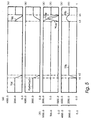
- the mode of operation of the circuit arrangement according to FIG. 4 when switching the power semiconductor switch on and off Th is based on the current and voltage profiles shown in FIG. 6 described in more detail.
- the load current iL initially flows in the freewheeling diode Df in series with the wiring choke Le2 to the load L.
- the wiring capacitor Ca is charged to zero, the wiring choke Le1, which is required anyway, acting as a switching choke.
- the load current iL first commutates via the wiring diode Db into the wiring capacitor Ca.
- the load current iL commutates into the path wiring diode D1 - storage capacitor Csp - wiring diode D2, whereby the storage capacitor Csp is connected in parallel with the wiring reactors Le1, Le2.
- the now increasing capacitor voltage causes a current commutation in the path freewheeling diode Df - wiring choke Le2.
- the load current iL flows into the freewheeling diode Df in series with the wiring choke Le2.
- the energy of both circuit chokes Le1, Le2 is first temporarily stored in the storage capacitor Csp and then fed back into the load L.
- the specified wiring arrangements can not only applied to buck converter according to Fig. 1 or Fig. 3 or Fig. 4 but also for other DC power controllers (Step-up and step-up / step-down converter) and their Derivatives (Cuk, SEPIC and ZETA controllers). Is too the procedure for various controllable power semiconductor switches (e.g. GTO thyristors, IGBT transistors, BJT transistors, MOSFET transistors, etc.) applicable.
Landscapes
- Dc-Dc Converters (AREA)
- Power Conversion In General (AREA)
Abstract
Description
- sie ein Einschaltentlastungsnetzwerk ohne prinzipbedingte Verluste aufweist,
- sie eine Kombination eines Ein- und Abschaltentlastungsnetzwerks ohne prinzipbedingte Verluste aufweist,
- ein möglichst geringer Aufwand an Bauelementen, insbesondere auch eine Rückspeisung der gespeicherten Energie ohne Verwendung zusätzlicher steuerbarer elektronischer Schalter erreicht wird und daß
- keine Einschränkung bezüglich der Höhe des abzuschaltenden Stromes besteht.
- Fig. 1
- eine Schaltungsanordnung zur Einschaltentlastung ohne prinzipbedingte Verluste am Beispiel eines Tiefsetzstellers,
- Fig. 2a
- eine unbeschaltete Freilaufdiode eines Gleichstomstellers nach dem Stande der Technik,
- Fig. 2b
- die Freilaufdiode nach Fig. 2a mit einem Einschaltentlastungsnetzwerk beschaltet,
- Fig. 3
- eine zwecks Abschaltentlastung erweiterte Schaltungsanordnung nach Fig. 1 ohne prinzipbedingte Schaltverluste,
- Fig. 4
- eine Variante zur Abschaltentlastung nach Fig. 3,
- Fig. 5
- die Strom- und Spannungsverläufe beim Ein- und Abschalten des elektronischen Schalters nach Fig. 1,
- Fig. 6
- die Strom- und Spannungsverläufe beim Ein- und Abschalten des elektronischen Schalters nach Fig. 4.
- Ca
- Beschaltungskondensator
- Csp
- Speicherkondensator
- Db, De, D1, D2
- Beschaltungsdioden
- Df
- Freilaufdiode
- Le1, Le2
- Beschaltungsdrosseln
- Th
- Leistungshalbleiterschalter
- iL
- Laststrom durch die Last L
- Ud
- Zwischenkreisgleichspannung
- uL
- Spannungsabfall über der Last L
- iDf
- Stromverlauf an Df
- iD1
- Stromverlauf an D1
- iLe1, iLe2
- Stromverläufe an Le1, Le2
- iCa, uCa
- Strom- und Spannungsverlauf an Ca
- iCsp, uCsp
- Strom- und Spannungsverlauf an Csp
- iTh, uTh
- Strom- und Spannungsverlauf an Th
Claims (10)
- Schaltungsanordnung zur Verlustleistungsentlastung eines Leistungshalbleiterschalters, der in Reihe mit einer Last im Zweig einer Gleichspannungsquelle liegt, wobei antiparallel zur Last eine Freilaufdiode angeordnet ist, insbesondere für Gleichstromsteller, dadurch gekennzeichnet, daß die Kathode der Freilaufdiode (Df) an die Kathode einer ersten Beschaltungsdiode (De) und an eine erste Beschaltungsdrossel (Le2) angeschlossen ist, daß an die Anode der Freilaufdiode (Df) die Anode einer zweiten Beschaltungsdiode (D2) und eine zweite Beschaltungsdrossel (Le1) angeschlossen ist, wobei die Kathode der zweiten Beschaltungsdiode (D2) mit dem anderen Anschluß der ersten Beschaltungsdrossel (Le2) und zusätzlich mit der Last (L) und der Gleichspannungsquelle (Ud) verbunden ist und die Anode der ersten Beschaltungsdiode (De) mit der Kathode einer dritten Beschaltungsdiode (D1) verbunden ist, deren Anode mit dem zweiten Anschluß der zweiten Beschaltungsdrossel (Le1) und mit der Anode des Leistungshalbleiterschalters (Th) verbunden ist und daß ein Speicherkondensator (Csp) zwischen die Anode der zweiten Beschaltungsdiode (D2) und die Kathode der dritten Beschaltungsdiode (D1) gelegt ist.
- Schaltungsanordnung zur Verlustleistungsentlastung eines Leistungshalbleiterschalters, der in Reihe mit einer Last im Zweig einer Gleichspannungsquelle liegt, wobei antiparallel zur Last eine zwecks Einschaltentlastung gemäß Anspruch 1 beschaltete Freilaufdiode liegt, dadurch gekennzeichnet, daß eine vierte Beschaltungsdiode (Db) anodenseitig zwischen dem Verbindungspunkt der Anode des Leistungshalbleiterschalters (Th) mit der zweiten Beschaltungsdrossel (Le1) uns kathodenseitig mit der Anode der dritten Beschaltungsdiode (D1) angeschlossen ist und ein Beschaltungskondensator (Ca) zwischen der Anode der dritten Beschaltungsdiode (D1) und der Kathode des Leistungshalbleiterschalters (Th) angeordnet ist.
- Schaltungsanordnung nach Anspruch 2, dadurch gekennzeichnet, daß die Last (L) an den gemeinsamen Verbindungspunkt von der zweiten Beschaltungsdiode (D2) mit der Freilaufdiode (Df), mit dem Speicherkondensator (Csp) und mit der zweiten Beschaltungsdrossel (Le1) liegt.
- Schaltungsanordnung nach einem der vorhergehenden Ansprüche, dadurch gekennzeichnet, daß der Leistungshalbleiterschalter ein Abschalt- (GTO)- Thyristor ist.
- Schaltungsanordnung nach einem der Ansprüche 1 bis 3, dadurch gekennzeichnet, daß der Leistungshalbleiterschalter als IGBT-Transitorstrecke ausgebildet ist.
- Schaltungsanordnung nach einem der Ansprüche 1 bis 3, dadurch gekennzeichnet, daß der Leistungshalbleiterschalter ein BJT-Transistor ist.
- Schaltungsanordnung nach einem der Ansprüche 1 bis 3, dadurch gekennzeichnet, daß der Leistungshalbleiterschalter ein MOSFET-Leistungstransistor ist.
- Schaltungsanordnung nach einem der vorhergehenden Ansprüche, dadurch gekennzeichnet, daß der Gleichstromsteller als Tiefsetzsteller und seinen Derivaten ausgeführt ist.
- Schaltungsanordnung nach einem der vorhergehenden Ansprüche, dadurch gekennzeichnet, daß der Gleichstromsteller als Hochsetzsteller und seinen Derivaten ausgeführt ist.
- Schaltungsanordnung nach einem der vorhergehenden Ansprüche, gekennzeichnet durch eine Ausführung als Hoch/Tiefsetzsteller und seiner Derivate.
Applications Claiming Priority (2)
| Application Number | Priority Date | Filing Date | Title |
|---|---|---|---|
| DE19735576A DE19735576C1 (de) | 1997-08-09 | 1997-08-09 | Schaltungsanordnung zur Verlustleistungsentlastung von Leistungshalbleiterschaltern in Gleichstromstellern |
| DE19735576 | 1997-08-09 |
Publications (3)
| Publication Number | Publication Date |
|---|---|
| EP0897219A2 true EP0897219A2 (de) | 1999-02-17 |
| EP0897219A3 EP0897219A3 (de) | 2000-05-24 |
| EP0897219B1 EP0897219B1 (de) | 2003-09-10 |
Family
ID=7839189
Family Applications (1)
| Application Number | Title | Priority Date | Filing Date |
|---|---|---|---|
| EP98250202A Expired - Lifetime EP0897219B1 (de) | 1997-08-09 | 1998-06-10 | Schaltungsanordnung zur Verlustleistungsentlastung von Leistungshalbleiterschaltern in Gleichstromstellern |
Country Status (3)
| Country | Link |
|---|---|
| EP (1) | EP0897219B1 (de) |
| DE (2) | DE19735576C1 (de) |
| ES (1) | ES2207791T3 (de) |
Family Cites Families (5)
| Publication number | Priority date | Publication date | Assignee | Title |
|---|---|---|---|---|
| AT300959B (de) * | 1970-06-12 | 1972-08-10 | Elin Union Ag | Schaltung zum Schutz der steuerbaren Ventile eines stromkommutierten Wechselrichters |
| DE2644715C2 (de) * | 1976-10-04 | 1985-02-28 | Andreas Prof. Dr.-Ing.habil. 7000 Stuttgart Boehringer | Einrichtung zur Befreiung elektrischer oder elektronischer Einwegschalter von hoher Verlustleistungsbeanspruchung während des Einschaltens - bei welchem ein, zuvor in einem anderen Schaltungspfad fließender, von Null verschiedener Strom auf den betreffenden Einwegschalter überwechselt - und von überhöhter Sperrspannungsbeanspruchung zum Ende des Ausschaltens |
| DE3120469C2 (de) * | 1981-05-20 | 1983-12-01 | Licentia Patent-Verwaltungs-Gmbh, 6000 Frankfurt | Schaltungsanordnung zur Entlastung elektronischer Zweigpaare von der Verlustenergie beim Ein- und Abschaltvorgang |
| JP2674341B2 (ja) * | 1991-03-27 | 1997-11-12 | 三菱電機株式会社 | 電力変換装置のスナバ回路 |
| DE19611707A1 (de) * | 1996-03-25 | 1997-10-02 | Patent Treuhand Ges Fuer Elektrische Gluehlampen Mbh | Gleichstromsteller |
-
1997
- 1997-08-09 DE DE19735576A patent/DE19735576C1/de not_active Expired - Fee Related
-
1998
- 1998-06-10 ES ES98250202T patent/ES2207791T3/es not_active Expired - Lifetime
- 1998-06-10 DE DE59809545T patent/DE59809545D1/de not_active Expired - Fee Related
- 1998-06-10 EP EP98250202A patent/EP0897219B1/de not_active Expired - Lifetime
Also Published As
| Publication number | Publication date |
|---|---|
| DE19735576C1 (de) | 1999-02-11 |
| EP0897219A3 (de) | 2000-05-24 |
| ES2207791T3 (es) | 2004-06-01 |
| EP0897219B1 (de) | 2003-09-10 |
| DE59809545D1 (de) | 2003-10-16 |
Similar Documents
| Publication | Publication Date | Title |
|---|---|---|
| EP1917712B1 (de) | Pulswiderstand (bremswiderstand) für einen umrichter im höheren spannungs- und leistungsbereich | |
| DE2834512C2 (de) | Umformer mit ausschaltbaren Thyristoren | |
| DE19746112A1 (de) | Stromrichteranordnung | |
| DE102011006769A1 (de) | Leistungsumwandlungsschaltung | |
| WO2003085818A1 (de) | Umrichtersystem, verfahren und umrichter | |
| EP2709257A2 (de) | Stromrichterschaltung und Verfahren zur Steuerung der Stromrichterschaltung | |
| DE69210940T2 (de) | Leistungsumrichter | |
| DE4428675A1 (de) | Schaltungsanordnung zum Schutz eines abschaltbaren Leistungshalbleiter-Schalters vor Überspannungen | |
| DE102014213737A1 (de) | Treiberschaltung und Halbleitervorrichtung, die die Treiberschaltung enthält | |
| EP0645889B1 (de) | Verfahren und Vorrichtung zur Begrenzung der Stromfallgeschwindigkeit beim Ausschalten von Leistungshalbleiterschaltern mit MOS-Steuereingang | |
| DE10020137A1 (de) | Verfahren und Schaltung zur Rückspeisung der in einer Stromrichterbeschaltung anfallenden elektrischen Energie | |
| DE3215589C2 (de) | ||
| EP1931023A1 (de) | Gleichstromversorgungssystem | |
| DE102024108537A1 (de) | Ansteuervorrichtung und leistungswandler | |
| DE102015105889A1 (de) | Schaltmodul und Umrichter mit wenigstens einem Schaltmodul | |
| EP0897219B1 (de) | Schaltungsanordnung zur Verlustleistungsentlastung von Leistungshalbleiterschaltern in Gleichstromstellern | |
| EP0751611A2 (de) | Stromrichterschaltungsanordnung | |
| DE4321988A1 (de) | Schaltungsanordnung für einen Zweipunkt-Wechselrichterschaltpol | |
| DE4042378C2 (de) | ||
| DE4430078A1 (de) | Schaltungsanordnung zur Vermeidung von Schaltverlusten eines Zweigpaares eines selbstgeführten Stromrichters mit eingeprägter Zwischenkreisgleichspannung | |
| DE19527178C1 (de) | Rückspeiseschaltung für eine Entlastungsschaltung für einen Zweipunkt- bzw. Dreipunkt-Ventilzweig | |
| EP0450126B1 (de) | Schutz- und Überwachungseinrichtung für eine Pulswiderstandsanordnung eines Spannungszwischenkreisumrichters | |
| AT390855B (de) | Schaltungsanordnung zur erzeugung einer aus phasenleitern und einem mittelpunktsleiter abgeleiteten stromversorgung fuer fehlerstromschutzschalter | |
| CH682611A5 (de) | Schaltentlastungsnetzwerk für einen Schalter und Verwendung desselben. | |
| DE3120469C2 (de) | Schaltungsanordnung zur Entlastung elektronischer Zweigpaare von der Verlustenergie beim Ein- und Abschaltvorgang |
Legal Events
| Date | Code | Title | Description |
|---|---|---|---|
| PUAI | Public reference made under article 153(3) epc to a published international application that has entered the european phase |
Free format text: ORIGINAL CODE: 0009012 |
|
| AK | Designated contracting states |
Kind code of ref document: A2 Designated state(s): DE ES FR IT |
|
| AX | Request for extension of the european patent |
Free format text: AL;LT;LV;MK;RO;SI |
|
| PUAL | Search report despatched |
Free format text: ORIGINAL CODE: 0009013 |
|
| AK | Designated contracting states |
Kind code of ref document: A3 Designated state(s): AT BE CH CY DE DK ES FI FR GB GR IE IT LI LU MC NL PT SE |
|
| AX | Request for extension of the european patent |
Free format text: AL;LT;LV;MK;RO;SI |
|
| 17P | Request for examination filed |
Effective date: 20000921 |
|
| AKX | Designation fees paid |
Free format text: DE ES FR IT |
|
| RAP1 | Party data changed (applicant data changed or rights of an application transferred) |
Owner name: DAIMLERCHRYSLER RAIL SYSTEMS GMBH |
|
| GRAH | Despatch of communication of intention to grant a patent |
Free format text: ORIGINAL CODE: EPIDOS IGRA |
|
| GRAH | Despatch of communication of intention to grant a patent |
Free format text: ORIGINAL CODE: EPIDOS IGRA |
|
| GRAA | (expected) grant |
Free format text: ORIGINAL CODE: 0009210 |
|
| AK | Designated contracting states |
Kind code of ref document: B1 Designated state(s): DE ES FR IT |
|
| REF | Corresponds to: |
Ref document number: 59809545 Country of ref document: DE Date of ref document: 20031016 Kind code of ref document: P |
|
| RAP2 | Party data changed (patent owner data changed or rights of a patent transferred) |
Owner name: BOMBARDIER TRANSPORTATION GMBH |
|
| REG | Reference to a national code |
Ref country code: ES Ref legal event code: FG2A Ref document number: 2207791 Country of ref document: ES Kind code of ref document: T3 |
|
| PG25 | Lapsed in a contracting state [announced via postgrant information from national office to epo] |
Ref country code: ES Free format text: LAPSE BECAUSE OF NON-PAYMENT OF DUE FEES Effective date: 20040611 |
|
| ET | Fr: translation filed | ||
| PLBE | No opposition filed within time limit |
Free format text: ORIGINAL CODE: 0009261 |
|
| 26N | No opposition filed |
Effective date: 20040614 |
|
| PG25 | Lapsed in a contracting state [announced via postgrant information from national office to epo] |
Ref country code: DE Free format text: LAPSE BECAUSE OF NON-PAYMENT OF DUE FEES Effective date: 20050101 |
|
| PG25 | Lapsed in a contracting state [announced via postgrant information from national office to epo] |
Ref country code: FR Free format text: LAPSE BECAUSE OF NON-PAYMENT OF DUE FEES Effective date: 20050228 |
|
| REG | Reference to a national code |
Ref country code: FR Ref legal event code: ST |
|
| PG25 | Lapsed in a contracting state [announced via postgrant information from national office to epo] |
Ref country code: IT Free format text: LAPSE BECAUSE OF NON-PAYMENT OF DUE FEES Effective date: 20050610 |
|
| REG | Reference to a national code |
Ref country code: ES Ref legal event code: FD2A Effective date: 20040611 |