EP0896417A2 - Circuit arrangement with a switching transistor - Google Patents
Circuit arrangement with a switching transistor Download PDFInfo
- Publication number
- EP0896417A2 EP0896417A2 EP98112685A EP98112685A EP0896417A2 EP 0896417 A2 EP0896417 A2 EP 0896417A2 EP 98112685 A EP98112685 A EP 98112685A EP 98112685 A EP98112685 A EP 98112685A EP 0896417 A2 EP0896417 A2 EP 0896417A2
- Authority
- EP
- European Patent Office
- Prior art keywords
- input
- temperature
- resistance
- circuit arrangement
- resistor
- Prior art date
- Legal status (The legal status is an assumption and is not a legal conclusion. Google has not performed a legal analysis and makes no representation as to the accuracy of the status listed.)
- Granted
Links
Images

Classifications
-
- H—ELECTRICITY
- H02—GENERATION; CONVERSION OR DISTRIBUTION OF ELECTRIC POWER
- H02M—APPARATUS FOR CONVERSION BETWEEN AC AND AC, BETWEEN AC AND DC, OR BETWEEN DC AND DC, AND FOR USE WITH MAINS OR SIMILAR POWER SUPPLY SYSTEMS; CONVERSION OF DC OR AC INPUT POWER INTO SURGE OUTPUT POWER; CONTROL OR REGULATION THEREOF
- H02M3/00—Conversion of dc power input into dc power output
- H02M3/02—Conversion of dc power input into dc power output without intermediate conversion into ac
- H02M3/04—Conversion of dc power input into dc power output without intermediate conversion into ac by static converters
- H02M3/10—Conversion of dc power input into dc power output without intermediate conversion into ac by static converters using discharge tubes with control electrode or semiconductor devices with control electrode
- H02M3/145—Conversion of dc power input into dc power output without intermediate conversion into ac by static converters using discharge tubes with control electrode or semiconductor devices with control electrode using devices of a triode or transistor type requiring continuous application of a control signal
- H02M3/155—Conversion of dc power input into dc power output without intermediate conversion into ac by static converters using discharge tubes with control electrode or semiconductor devices with control electrode using devices of a triode or transistor type requiring continuous application of a control signal using semiconductor devices only
- H02M3/156—Conversion of dc power input into dc power output without intermediate conversion into ac by static converters using discharge tubes with control electrode or semiconductor devices with control electrode using devices of a triode or transistor type requiring continuous application of a control signal using semiconductor devices only with automatic control of output voltage or current, e.g. switching regulators
Abstract
Description
Die Erfindung bezieht sich auf eine Schaltungsanordnung mit einem in einem ersten Schaltungsabschnitt angeordneten Schalttransistor, der über eine ein Steuerglied aufweisende Ansteuereinheit zur Abgabe eines vorgegebenen oder vorgebbaren Ausgangsstroms intermittierend angesteuert wird.The invention relates to a circuit arrangement with one in a first Circuit section arranged switching transistor, which has a control element Control unit for delivering a predetermined or predeterminable output current is controlled intermittently.
Eine Schaltungsanordnung dieser Art ist in der DE-Z "Elektor", 4/93, Seiten 41, 42, 47 und 48 angegeben. Um den Schalttransistor in Form eines Feldeffekttransistors gegen zu hohe Verlustleistung zu schützen, ist ein Widerstand mit negativem Temperaturkoeffizienten, d.h. ein NTC-Widerstand vorgesehen, der mit dem Leistungstransistor in engem thermischem Kontakt steht, um ihn bei zu hoher Verlustleistung abzuschalten. Ein derartiges Abschalten ist in vielen Fällen ungeeignet. Ähnlich wirkt auch ein auf Seite 48 dieser Literaturstelle angegebener Temperatursensor.A circuit arrangement of this type is in DE-Z "Elektor", 4/93, pages 41, 42, 47 and 48 specified. To the switching transistor in the form of a field effect transistor against too high Protecting power loss is a resistor with a negative temperature coefficient, i.e. a NTC resistor provided that is in close thermal contact with the power transistor is to switch it off if the power loss is too high. Such a shutdown is in many Cases unsuitable. A reference given on page 48 of this literature reference has a similar effect Temperature sensor.
Der Erfindung liegt die Aufgabe zugrunde, eine Schaltungsanordnung der eingangs genannten Art bereitzustellen, deren Ausgangsstrom temperaturkompensiert auf einem vorgegebenen Wert gehalten wird. The invention has for its object a circuit arrangement of the aforementioned Provide type whose output current is temperature compensated to a predetermined value is held.
Diese Aufgabe wird mit den im Patentanspruch 1 angegebenen Merkmalen gelöst. Hiernach ist also vorgesehen, daß einem Eingang des Steuerglieds ein von dem Bahnwiderstand des Schalttransistors beeinflußtes Signal zugeführt ist, und daß einem anderen Eingang des Steuerglieds zum Bestimmen des Tastverhältnisses der intermittierenden Ansteuerung ein Steuersignal zugeführt ist, das mit einem dem Temperaturverlauf des Bahnwiderstandes entgegenwirkenden Temperaturverlauf beaufschlagt ist.This object is achieved with the features specified in claim 1. Accordingly, it is provided that an input of the control element is one of the rail resistance of the switching transistor influenced signal is supplied, and that another input of the Control element for determining the duty cycle of the intermittent control Control signal is supplied, which with a the temperature profile of the sheet resistance counteracting temperature profile is applied.
Durch die Zuführung des von dem Bahnwiderstand des Schalttransistors beeinflußten Signals zu dem einen Eingang und dem Steuersignal, das mit einem dem Temperaturverlauf des Bahnwiderstandes entgegenwirkenden Temperaturverlauf beaufschlagt ist, zu dem anderen Eingang des Steuerglieds wird das Ausgangssignal des Steuerglieds temperaturunabhängig und der von der Ansteuereinheit bestimmte Ausgangsstrom zum temperaturunabhängigen Betrieb einer Last auf einem von der Temperatur unbeeinflußten, stabilen Wert gehalten. Eine derartige Schaltung ist z.B. gut geeignet für die Ansteuerung einer Entladungslampe, die lediglich in der Anfangsphase eine erhöhte Anlaufleistung benötigt und danach in den erheblich weniger Leistung erfordernden Brennbetrieb übergeht.By supplying the signal influenced by the path resistance of the switching transistor the one input and the control signal, which with a the temperature curve of the Path resistance counteracting temperature profile is applied to the other Input of the control element, the output signal of the control element becomes independent of temperature and the output current determined by the control unit for temperature-independent operation a load is kept at a stable value which is not influenced by the temperature. Such Circuit is e.g. well suited for the control of a discharge lamp, which is only in the In the initial phase an increased start-up power is required and afterwards in the considerably less Burning operation requiring power passes.
Ist vorgesehen, daß als Steuerglied eine Vergleicherstufe vorgesehen ist, und daß das Steuersignal an dem anderen Eingang durch einen in Abhängigkeit der Temperatur variierten Widerstandswert eines Widerstandsnetzwerks beaufschlagt ist, so wird die Temperaturkompensation mit einfachen Mitteln erzielt.It is provided that a comparator stage is provided as a control element, and that Control signal at the other input by a variable depending on the temperature Resistance value of a resistance network is applied, then the Temperature compensation achieved with simple means.
Dabei bestehen einfache Maßnahmen darin, daß der Bahnwiderstand parallel zu einem ersten Eingangswiderstand an den einen Eingang der Vergleicherstufe angeschlossen ist und daß an dem anderen Eingang ein Spannungsteiler aus einem weiteren Eingangswiderstand und aus einer Widerstandsgruppe mit einem temperaturabhängigen Widerstand angeschlossen ist, wobei der temperaturabhängige Widerstand leicht entsprechend einer geeigneten Kompensationskurve für den Bahnwiderstand gewählt werden kann. Insbesondere kann dabei vorgesehen sein, daß der Bahnwiderstand positiven und der temperaturabhängige Widerstand negativen Temperaturkoeffizienten besitzt und daß der eine Eingang der invertierende und der andere Eingang der nichtinvertierende Eingang der Vergleicherstufe sind. Der positive Temperaturkoeffizient des Bahnwiderstandes wird kompensiert durch den negativen Temperaturkoeffizienten des temperaturabhängigen NTC-Widerstandes. Simple measures consist in the fact that the sheet resistance is parallel to a first Input resistance is connected to one input of the comparator stage and that to the other input a voltage divider from another input resistor and from one Resistor group with a temperature-dependent resistor is connected, the temperature dependent resistance easily according to a suitable compensation curve for the rail resistance can be selected. In particular, it can be provided that the Path resistance positive and the temperature-dependent resistance negative temperature coefficient has and that one input the inverting and the other input the are non-inverting input of the comparator stage. The positive temperature coefficient of the Railway resistance is compensated for by the negative temperature coefficient of the temperature-dependent NTC resistor.
Ein alternativer Aufbau ist dadurch gekennzeichnet, daß der Bahnwiderstand parallel zu einem ersten Eingangswiderstand an den einen Eingang der Vergleicherstufe angeschlossen ist, daß an dem anderen Eingang ein Spannungsteiler aus einem weiteren Eingangswiderstand und aus einer weiteren Widerstandsgruppe angeschlossen ist und daß der Widerstandswert der weiteren Widerstandsgruppe durch unterschiedliche Kombination in Abhängigkeit der Temperatur zugeschalteter und abgetrennter Widerstände variierbar ist. Auch dieser Aufbau ist mit relativ wenig Aufwand verbunden, wobei die Änderung des Bahnwiderstandes mit der Temperatur durch eine gegenläufige Änderung des Widerstandswertes der weiteren Widerstandsgruppe über der Temperatur kompensiert wird. Um dabei die Steuerung der weiteren Widerstandsgruppe entsprechend der den Bahnwiderstand beeinflussenden Umgebungstemperatur genau vorzunehmen, ist vorteilhaft vorgesehen, daß ein Temperaturfühler vorgesehen ist, der eine den Bahnwiderstand beeinflussende Umgebungstemperatur möglichst genau erfaßt, und daß die Kombination der Widerstände in Abhängigkeit des erfaßten Temperatursignals gesteuert wird. Der Temperaturfühler steht dabei in möglichst enger thermischer Beziehung zu dem Bahnwiderstand.An alternative construction is characterized in that the sheet resistance is parallel to one first input resistor is connected to the one input of the comparator stage that at the other input a voltage divider consisting of another input resistor and out another resistance group is connected and that the resistance value of the other Resistance group through different combinations depending on the temperature connected and disconnected resistors is variable. This structure is also relative little effort connected, the change in the sheet resistance with the temperature by an opposite change in the resistance value of the further resistance group the temperature is compensated. To control the further resistance group according to the ambient temperature influencing the sheet resistance to make, it is advantageously provided that a temperature sensor is provided, the one Ambient temperature influencing the rail resistance recorded as precisely as possible, and that the Combination of the resistors is controlled depending on the detected temperature signal. The temperature sensor is in the closest possible thermal relationship to that Railway resistance.
Das Steuersignal an dem anderen Eingang des Steuerglieds wird zur Vorgabe des Ausgangsstroms beispielsweise dadurch in dem von der Last benötigten zeitlichen Verlauf genau bereitstellbar, daß das Steuersignal an dem anderen Eingang des Steuergliedes von einer zentralen Steuerungseinheit bereitgestellt wird.The control signal at the other input of the control element is used to specify the Output current, for example, exactly in the time course required by the load can be provided that the control signal at the other input of the control element from one central control unit is provided.
Eine weitere alternative Ausführungsform besteht darin; daß das Steuersignal in der zentralen Steuerungseinheit mittels eines Programms in Abhängigkeit von den Eigenschaften des Schalttransistors und der Temperatur im Bereich des Bahnwiderstands erzeug wird. Das dem anderen Eingang des Steuerglieds zugeführte Steuersignal wird dabei auf einfache Weise und den jeweiligen Erfordernissen genau angepaßt durch Software erzeugt, wobei die Eigenschaften des jeweiligen Schalttransistors und gewünschtenfalls weitere Eigenschaften der Schaltung mit einfachen Maßnahmen ohne schaltungstechnische Änderungen am Eingang des Steuerglieds berücksichtigt werden können. Auch kann ein jeweiliges gewünschtes Regelverhalten mit der zentralen Steuerungseinheit vorgegeben werden, so daß Eigenarten beim Betreiben der Last in Verbindung mit dem Temperaturverlauf des Bahnwiderstandes ebenfalls berücksichtigt werden können. Another alternative embodiment is; that the control signal in the central Control unit using a program depending on the properties of the switching transistor and the temperature is generated in the area of the sheet resistance. The other Input of the control element supplied control signal is simple and the respective Tailored to requirements by software, the characteristics of the respective switching transistor and, if desired, further properties of the circuit simple measures without changes in circuitry at the input of the control element can be taken into account. A respective desired control behavior can also be achieved with the central control unit can be specified so that peculiarities when operating the load in Connection with the temperature profile of the sheet resistance are also taken into account can.
Die Erfindung wird nachfolgend anhand von Ausführungsbeispielen unter Bezugnahme auf die Zeichnungen näher dargestellt. Es zeigen:
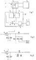
- Fig. 1
- ein Blockschaltbild einer Schaltungsanordnung mit einem Schalttransistor und Temperaturkompensation,
- Fig. 2
- ein erstes Ausführungsbeispiel für die Temperaturkompensation
- Fig. 3
- ein weiteres Ausführungsbeispiel für die Temperaturkompensation und
- Fig. 4
- ein weiteres Ausführungsbeispiel für die Temperaturkompensation.
- Fig. 1
- 2 shows a block diagram of a circuit arrangement with a switching transistor and temperature compensation,
- Fig. 2
- a first embodiment for temperature compensation
- Fig. 3
- another embodiment for temperature compensation and
- Fig. 4
- another embodiment for temperature compensation.
Die in Fig. 1 als Blockschaltbild dargestellte Schaltungsanordnung weist in ihrem oberen, ersten Schaltungsabschnitt einen beispielsweise an eine Autobatterie angeschlossenen DC/DC-Wandler 1 mit einem Schalttransistor 1.1 in Form eines Feldeffekt-Schalttransistors auf. An den DC/DC-Wandler ist eine zu betreibende Last 2, wie z.B. eine Entladungslampe angeschaltet.The circuit arrangement shown as a block diagram in FIG. 1 has in its upper, first one Circuit section connected, for example, to a car battery DC / DC converter 1 with a switching transistor 1.1 in the form of a field-effect switching transistor. A load 2 to be operated is connected to the DC / DC converter, e.g. a discharge lamp switched on.
Der DC/DC-Wandler 1 mit dem Schalttransistor 1.1 wird mit einer darunter dargestellten
Ansteuereinheit 10 mit einer Ansteuerschaltung 3, einem Steuerglied in Form einer
Vergleicherstufe 5, einer Bewertungsschaltung 4 und einer Pegeleinstellstufe 6 intermittierend
angesteuert, um den Ausgangsstrom für die Last 2 nach Bedarf vorzugeben. Der erforderliche
Ausgangsstrom wird mit einem Steuersignal einer zentralen Steuerungseinheit in Form eines
Mikroprozessors bzw. Mikrocontrollers 7 gesteuert.The DC / DC converter 1 with the switching transistor 1.1 is shown with one below
Je nach dem Ausgangsstrom, der der Last 2 bereitgestellt werden muß und z.B. bei eine Lampe
in der anfänglichen Anlaufphase während der ersten 20 sec. eine erheblich höhere Leistung
aufnimmt als in der daran anschließenden stabilen Brennphase, wird mit dem von dem
Mikrocontroller 7 bestimmten Steuersignal eine Schaltschwelle an der Vergleicherstufe 5
vorgegeben. Dazu wird dem einen Eingang a der Vergleicherstufe 5 ein Signal von dem
Schalttransistor 1.1 über die Bewertungsschaltung 4 zugeführt, während dem anderen Eingang
b der Vergleicherstufe 5 das Steuersignal über die Pegeleinstellstufe 6 zugeführt wird. Das
Tastverhältnis des von der Vergleicherstufe 5 ausgegebenen Signals hängt zum einen von dem
z.B. dreieckförmigen oder trapezförmigen Signal an dem einen Eingang a und zum anderen von
dem Pegel des Steuersignals an dem anderen Eingang b ab, und das von der Vergleicherstufe 5
ausgegebene Signal wird über die Ansteuerschaltung 3 dem Gate-Anschluß des Feldeffekt-Schalttransistors
1.1 zugeführt.Depending on the output current that must be provided to load 2 and e.g. at a lamp
in the initial start-up phase during the first 20 sec. a significantly higher performance
records than in the subsequent stable burning phase, is with that of the
Das über die Bewertungsschaltung 4 dem einen Eingang a der Vergleicherstufe 5 zugeführte
Signal hängt von dem Wert des Bahnwiderstandes des Feldeffekt-Schalttransistors 1.1 ab, der
seinerseits temperaturabhängig ist und z.B. bei -50 °C gegenüber Zimmertemperatur um den
Faktor 0,6 niedriger ist, wahrend er bei 130 °C gegenüber Zimmertemperatur um den Faktor 2
größer ist. Je nach Typ beträgt der Bahnwiderstand bei Zimmertemperatur z.B. einige 10mΩ.
Aufgrund der Temperaturabhängigkeit kann der von dem Mikrocontroller 7 über die
Ansteuereinheit 10 bestimmte Ausgangsstrom stark verfälscht sein, so daß z.B. der von der
Autobatterie entnommene Strom an Kabelbaumwiderständen und Übergangswiderständen von
Kontakten einen erheblichen Spannungsabfall bewirkt, so daß die benötigte minimale
Versorgungsspannung für die Schaltungsanordnung unterschritten werden kann. Auch andere
negative Einflüsse auf die ordnungsgemäße Funktion der Schaltungsanordnung können sich
durch die Änderung des Bahnwiderstandes ergeben.That fed via the
Um trotz Temperaturänderungen, die beispielsweise bei einer Lampenansteuerung insbesondere in der Anfangsphase durch eine hohe Verlustleistung auftreten können, einen von der Temperatur unabhängigen, stabilen Ausgangsstrom zu gewährleisten, sind vorliegend Maßnahmen ergriffen, mit denen der Beeinflussung des Ausgangsstroms durch Temperaturänderung entgegengewirkt wird.In order in spite of temperature changes, for example in the case of a lamp control can occur in the initial phase due to high power dissipation, one depending on the temperature Measures are to be taken to ensure an independent, stable output current seized to influence the output current by changing the temperature is counteracted.
In Fig. 2 ist ein erstes Ausführungsbeispiel gezeigt. Das von dem Feldeffekt-Schalttransistor 1.1
abgeleitete, von dem Bahnwiderstand beeinflußte Signal wird dem einen Eingang a in Form des
invertierenden Eingangs der Vergleicherstufe 5 zugeführt und ist über einen Eingangswiderstand
R1 an Masse gelegt. Wird die Bewertungsschaltung 4 als Knoten betrachtet, so liegt, wie aus
den Fig. 1 und 2 ersichtlich ist, der Eingangswiderstand R1 parallel zu dem Bahnwiderstand des
Feldeffekt-Schalttransistors 1.1 gegen Masse. Bei einer Erhöhung des Bahnwiderstandes infolge
Temperaturerhöhung erhöht sich somit auch der an der Parallelschaltung des Bahnwiderstandes
und des Eingangswiderstandes R1 abfallende Spannungspegel, d.h. die Spannung an dem einen
Eingang a. Dieser durch die Temperaturänderung hervorgerufenen Spannungsänderung wird
dadurch entgegengewirkt, daß entsprechend der Änderung des Bahnwiderstandes mit der
Temperatur an dem anderen, nichtinvertierenden Eingang b der Vergleicherstufe 5 die an einem
Widerstandsnetzwerk aus Widerständen R2 bis R6 abfallende Spannung ebenfalls angehoben
wird, indem eine geeignete Kombination von Widerständen R4 bis R6 in Abhängigkeit der
Temperaturänderung geschaltet wird. Dazu ist ein nicht gezeigter Temperaturfühler in möglichst
enger thermischer Verbindung zu dem Bahnwiderstand des Feldeffekt-Schalttransistors 1.1
vorgesehen, der ein Temperatursignal an den Mikrocontroller 7 abgibt. Über jeweils zugeordnete
Ausgänge des Mikrocontrollers 7 wird die Kombination der Widerstände R4 bis R6 gewählt, so
daß sich im Zusammenwirken mit dem Widerstand R3 und dem anderen Eingangswiderstand R2
ein geeigneter Spannungsteilerwert ergibt. Über den Widerstand R3 wird vom Mikrocontroller 7
aus der Sollwert für den Ausgangsstrom vorgegeben.A first exemplary embodiment is shown in FIG. That of the field effect switching transistor 1.1
derived, influenced by the rail resistance signal is the one input a in the form of
inverting input of the comparator stage 5 and is via an input resistor
R1 grounded. If the
Ein weiteres Ausführungsbeispiel für eine Temperaturkompensation des Bahnwiderstandes des
Feldeffekt-Schalttransistors 1.1 ist in Fig. 3 wiedergegeben. Entsprechend dem
Ausführungsbeispiel nach Fig. 2 wird das von dem Feldeffekt-Schalttransistor 1.1 abgeleitete
Signal über die Bewertungsschaltung 4 dem invertierenden einen Eingang a der Vergleicherstufe
5 zugeführt, so daß der Bahnwiderstand auch hierbei parallel gegebenenfalls mit anderen
Schaltungskomponenten zu dem einen Eingangswiderstand R1 Iiegt. Der an dem einen Eingang
a erzeugte Spannungspegel wird demgemäß in der vorstehend beschriebenen Weise durch eine
temperaturabhängige Widerstandsänderung des Bahnwiderstandes beeinflußt. Zur Kompensation
ist an dem anderen, nichtinvertierenden Eingang b der Vergleicherstufe 5 ein Spannungsteiler
aus Widerständen R7, R8, R9 und NTC angeschlossen.Another embodiment for a temperature compensation of the sheet resistance of the
Field-effect switching transistor 1.1 is shown in Fig. 3. According to that
2 is derived from the field-effect switching transistor 1.1
Signal via the
Das Steuersignal des Mikrocontrollers 7 wird über diesen Spannungsteiler dem anderen Eingang
b der Vergleicherstufe 5 zugeführt. Der temperaturabhängige Widerstand NTC ist in möglichst
enger thermischer Nähe zu dem Bahnwiderstand des Feldeffekt-Schalttransistors 1.1 angeordnet
und wird demnach gegenläufig zu dem Bahnwiderstand bei Temperaturerhöhung herabgesetzt
bzw. bei Temperaturerniedrigung vergrößert. Dadurch erhöht sich bei höherer Temperatur auch
der Spannungspegel an dem anderen Eingang b der Vergleicherstufe 5, so daß auch hierbei ein
von der Temperatur unabhängiges Tastverhältnis an dem Ausgang der Vergleicherstufe 5 und
damit ein von einer Temperatur unabhängiger, konstanter Ausgangsstrom erzielt wird. Der
temperaturabhängige Widerstand NTC ist entsprechend dem Temperaturverlauf des Bahnwiderstandes
zur Kompensation geeignet gewählt. The control signal of the
Entsprechend den beschriebenen Ausführungsbeispielen sind auch ähnliche Schaltungen am Eingang der Vergleicherstufe 5 denkbar, mit denen der Änderung des Bahnwiderstandes in Abhängigkeit von der Temperatur entgegengewirkt werden kann, indem der Spannungspegel an dem anderen Eingang b der Vergleicherstufe 5 zur Kompensation der Temperaturdrift des Bahnwiderstandes geeignet in Abhängigkeit der Temperatur beeinflußt wird.In accordance with the exemplary embodiments described, there are also similar circuits at the input the comparator stage 5 conceivable, with which the change in the rail resistance depending of the temperature can be counteracted by the voltage level on the other input b of the comparator stage 5 to compensate for the temperature drift of the Path resistance is influenced depending on the temperature.
Bei einer in Fig. 4 gezeigten weiteren Ausführungsform der Schaltungsanordnung ist an dem
anderen Eingang b des Steuerglieds in Form der Vergleicherstufe 5 unmittelbar oder über ein geeignetes
Filterglied, das zum Beispiel einen Speicherkondensator und einen Widerstand aufweist,
eine zentrale Steuerungseinheit 7 angeschlossen. Mit der zentralen Steuerungseinheit 7 kann das
kompensierende Steuersignal auf einfache Weise mittels eines Programms in Abhängigkeit von
dem Temperaturverlauf des Bahnwiderstandes des Schalttransistors 1.1 für die jeweils vorherrschende
Temperatur erzeugt werden. Die Temperatur wird mittels eines geeigneten Temperaturfühlers
erfaßt, wie in Fig. 4 mit einem Pfeil angedeutet. Mit der zentralen Steuerungseinheit 7 ist
es auch möglich, ein günstiges Regelverhalten für die Ansteuerung der Last 2 jeweils unter Berücksichtigung
der vorliegenden Temperatur einzustellen. Beispielsweise kann zum Ansteuern
einer Endladungslampe das Regelverhalten in der Anlaufphase und während des Brennbetriebs
mit dem Programm geeignet gewählt werden.In a further embodiment of the circuit arrangement shown in FIG
other input b of the control element in the form of comparator stage 5 directly or via a suitable one
Filter element, which has, for example, a storage capacitor and a resistor,
a
Claims (8)
dadurch gekennzeichnet,
characterized,
dadurch gekennzeichnet,
characterized,
dadurch gekennzeichnet,
characterized,
dadurch gekennzeichnet,
characterized,
dadurch gekennzeichnet,
characterized,
dadurch gekennzeichnet,
characterized,
dadurch gekennzeichnet,
characterized,
dadurch gekennzeichnet,
characterized,
Applications Claiming Priority (2)
| Application Number | Priority Date | Filing Date | Title |
|---|---|---|---|
| DE19734410A DE19734410A1 (en) | 1997-08-08 | 1997-08-08 | Circuit arrangement with a switching transistor |
| DE19734410 | 1997-08-08 |
Publications (3)
| Publication Number | Publication Date |
|---|---|
| EP0896417A2 true EP0896417A2 (en) | 1999-02-10 |
| EP0896417A3 EP0896417A3 (en) | 2000-12-20 |
| EP0896417B1 EP0896417B1 (en) | 2002-12-04 |
Family
ID=7838414
Family Applications (1)
| Application Number | Title | Priority Date | Filing Date |
|---|---|---|---|
| EP98112685A Expired - Lifetime EP0896417B1 (en) | 1997-08-08 | 1998-07-09 | Circuit arrangement with a switching transistor |
Country Status (2)
| Country | Link |
|---|---|
| EP (1) | EP0896417B1 (en) |
| DE (2) | DE19734410A1 (en) |
Cited By (3)
| Publication number | Priority date | Publication date | Assignee | Title |
|---|---|---|---|---|
| WO2003017454A1 (en) * | 2001-08-21 | 2003-02-27 | Intersil Americas Inc. | Thermal compensation method and device for circuits with temperature-dependent current sensing elements |
| EP1424766A1 (en) * | 2002-11-29 | 2004-06-02 | STMicroelectronics S.r.l. | Switching voltage regulator |
| USRE42307E1 (en) | 2001-08-21 | 2011-04-26 | Intersil Americas Inc. | Thermally compensated current sensing of intrinsic power converter elements |
Families Citing this family (1)
| Publication number | Priority date | Publication date | Assignee | Title |
|---|---|---|---|---|
| DE102012215338A1 (en) | 2012-08-29 | 2014-03-06 | Robert Bosch Gmbh | Starter for starting combustion engine of vehicle, has switch comprising contact elements that are in contact with switching bridge, and pyroelectric conductor material with electrical resistance in specific range at room temperature |
Citations (3)
| Publication number | Priority date | Publication date | Assignee | Title |
|---|---|---|---|---|
| JPS6489916A (en) * | 1987-09-28 | 1989-04-05 | Mitsubishi Electric Corp | Output protection device |
| EP0464909A1 (en) * | 1990-06-29 | 1992-01-08 | Koninklijke Philips Electronics N.V. | Integrated circuit with co-integrated power supply reduction |
| EP0665629A2 (en) * | 1994-01-28 | 1995-08-02 | Canon Kabushiki Kaisha | Power control device and image forming apparatus utilizing the same |
Family Cites Families (2)
| Publication number | Priority date | Publication date | Assignee | Title |
|---|---|---|---|---|
| US3777187A (en) * | 1972-05-01 | 1973-12-04 | Love Controls Corp | Controller circuit |
| CA1045217A (en) * | 1976-02-10 | 1978-12-26 | Glenn A. Pollitt | Constant impedance mosfet switch |
-
1997
- 1997-08-08 DE DE19734410A patent/DE19734410A1/en not_active Ceased
-
1998
- 1998-07-09 DE DE59806500T patent/DE59806500D1/en not_active Expired - Lifetime
- 1998-07-09 EP EP98112685A patent/EP0896417B1/en not_active Expired - Lifetime
Patent Citations (3)
| Publication number | Priority date | Publication date | Assignee | Title |
|---|---|---|---|---|
| JPS6489916A (en) * | 1987-09-28 | 1989-04-05 | Mitsubishi Electric Corp | Output protection device |
| EP0464909A1 (en) * | 1990-06-29 | 1992-01-08 | Koninklijke Philips Electronics N.V. | Integrated circuit with co-integrated power supply reduction |
| EP0665629A2 (en) * | 1994-01-28 | 1995-08-02 | Canon Kabushiki Kaisha | Power control device and image forming apparatus utilizing the same |
Non-Patent Citations (1)
| Title |
|---|
| PATENT ABSTRACTS OF JAPAN vol. 013, no. 323 (E-791), 21. Juli 1989 (1989-07-21) & JP 01 089916 A (MITSUBISHI ELECTRIC CORP), 5. April 1989 (1989-04-05) * |
Cited By (6)
| Publication number | Priority date | Publication date | Assignee | Title |
|---|---|---|---|---|
| WO2003017454A1 (en) * | 2001-08-21 | 2003-02-27 | Intersil Americas Inc. | Thermal compensation method and device for circuits with temperature-dependent current sensing elements |
| US6687105B2 (en) | 2001-08-21 | 2004-02-03 | Intersil Americas Inc. | Thermal compensation method and device for circuits with temperature-dependent current sensing elements |
| CN100336289C (en) * | 2001-08-21 | 2007-09-05 | 英特赛尔美国股份有限公司 | Thermal compensation method and device for circuits with temperature-dependent current sensing elements |
| USRE42307E1 (en) | 2001-08-21 | 2011-04-26 | Intersil Americas Inc. | Thermally compensated current sensing of intrinsic power converter elements |
| EP1424766A1 (en) * | 2002-11-29 | 2004-06-02 | STMicroelectronics S.r.l. | Switching voltage regulator |
| US6998827B2 (en) | 2002-11-29 | 2006-02-14 | Stmicroelectronics S.R.L. | Switching voltage regulator with negative temperature compensation |
Also Published As
| Publication number | Publication date |
|---|---|
| DE19734410A1 (en) | 1999-02-11 |
| EP0896417B1 (en) | 2002-12-04 |
| DE59806500D1 (en) | 2003-01-16 |
| EP0896417A3 (en) | 2000-12-20 |
Similar Documents
| Publication | Publication Date | Title |
|---|---|---|
| DE102018006054A1 (en) | Device for at least partially discharging an electrical energy store | |
| EP0421516B1 (en) | Power supply arrangement with voltage regulation and current limiting | |
| DE112007001293T5 (en) | Power supply controller | |
| DE102006029190A1 (en) | Overcurrent detection device | |
| EP0762258A2 (en) | Circuit for driving a heating resistor | |
| DE112006002885B4 (en) | Power supply controller | |
| EP0901057B1 (en) | Current regulation circuit | |
| DE4115295C2 (en) | ||
| DE4005813C2 (en) | Device for monitoring the load current of an electronically switched consumer | |
| EP0896417B1 (en) | Circuit arrangement with a switching transistor | |
| DE3118240A1 (en) | INDICATOR | |
| EP0309753A1 (en) | Method for monitoring an inductive load | |
| DE112006002710B4 (en) | PWM signal generator | |
| DE2539117C3 (en) | Method and device for charging an electrical storage heater | |
| DD277562A1 (en) | CIRCUIT FOR CURRENT LIMITATION WITH FOLDBACK BEHAVIOR | |
| DE3519791C2 (en) | ||
| EP1047286B1 (en) | Ballast for discharge lamp in automobile | |
| DE4113258A1 (en) | Analog power control circuitry - has short circuit protection circuit limiting control output signal for each voltage value | |
| EP0164774A1 (en) | Circuit device for controlling the running voltage of high-pressure gas-discharge lamps | |
| DE71366T1 (en) | LAMP OPERATING CIRCUIT. | |
| DE2733006C3 (en) | Temperature monitor | |
| DE1513364A1 (en) | High current regulator with negative resistance | |
| WO2019076608A1 (en) | Circuit arrangement for generating a reference voltage for the power supply of an led arrangement | |
| DE19604042C1 (en) | Open-circuit load detection circuit e.g. for motor vehicle lighting circuit | |
| DE19711364A1 (en) | Voltage stabiliser for voltage supply device of motor vehicle |
Legal Events
| Date | Code | Title | Description |
|---|---|---|---|
| PUAI | Public reference made under article 153(3) epc to a published international application that has entered the european phase |
Free format text: ORIGINAL CODE: 0009012 |
|
| AK | Designated contracting states |
Kind code of ref document: A2 Designated state(s): DE ES FR GB IT |
|
| AX | Request for extension of the european patent |
Free format text: AL;LT;LV;MK;RO;SI |
|
| RTI1 | Title (correction) |
Free format text: CIRCUIT ARRANGEMENT WITH A SWITCHING TRANSISTOR |
|
| PUAL | Search report despatched |
Free format text: ORIGINAL CODE: 0009013 |
|
| AK | Designated contracting states |
Kind code of ref document: A3 Designated state(s): AT BE CH CY DE DK ES FI FR GB GR IE IT LI LU MC NL PT SE |
|
| AX | Request for extension of the european patent |
Free format text: AL;LT;LV;MK;RO;SI |
|
| 17P | Request for examination filed |
Effective date: 20010620 |
|
| AKX | Designation fees paid |
Free format text: DE ES FR GB IT |
|
| GRAG | Despatch of communication of intention to grant |
Free format text: ORIGINAL CODE: EPIDOS AGRA |
|
| GRAG | Despatch of communication of intention to grant |
Free format text: ORIGINAL CODE: EPIDOS AGRA |
|
| GRAH | Despatch of communication of intention to grant a patent |
Free format text: ORIGINAL CODE: EPIDOS IGRA |
|
| 17Q | First examination report despatched |
Effective date: 20020116 |
|
| GRAH | Despatch of communication of intention to grant a patent |
Free format text: ORIGINAL CODE: EPIDOS IGRA |
|
| GRAA | (expected) grant |
Free format text: ORIGINAL CODE: 0009210 |
|
| AK | Designated contracting states |
Kind code of ref document: B1 Designated state(s): DE ES FR GB IT |
|
| PG25 | Lapsed in a contracting state [announced via postgrant information from national office to epo] |
Ref country code: IT Free format text: LAPSE BECAUSE OF FAILURE TO SUBMIT A TRANSLATION OF THE DESCRIPTION OR TO PAY THE FEE WITHIN THE PRESCRIBED TIME-LIMIT;WARNING: LAPSES OF ITALIAN PATENTS WITH EFFECTIVE DATE BEFORE 2007 MAY HAVE OCCURRED AT ANY TIME BEFORE 2007. THE CORRECT EFFECTIVE DATE MAY BE DIFFERENT FROM THE ONE RECORDED. Effective date: 20021204 Ref country code: GB Free format text: LAPSE BECAUSE OF FAILURE TO SUBMIT A TRANSLATION OF THE DESCRIPTION OR TO PAY THE FEE WITHIN THE PRESCRIBED TIME-LIMIT Effective date: 20021204 |
|
| REG | Reference to a national code |
Ref country code: GB Ref legal event code: FG4D Free format text: NOT ENGLISH |
|
| REF | Corresponds to: |
Ref document number: 59806500 Country of ref document: DE Date of ref document: 20030116 |
|
| GBV | Gb: ep patent (uk) treated as always having been void in accordance with gb section 77(7)/1977 [no translation filed] |
Effective date: 20021204 |
|
| PG25 | Lapsed in a contracting state [announced via postgrant information from national office to epo] |
Ref country code: ES Free format text: LAPSE BECAUSE OF FAILURE TO SUBMIT A TRANSLATION OF THE DESCRIPTION OR TO PAY THE FEE WITHIN THE PRESCRIBED TIME-LIMIT Effective date: 20030627 |
|
| ET | Fr: translation filed | ||
| PGFP | Annual fee paid to national office [announced via postgrant information from national office to epo] |
Ref country code: FR Payment date: 20030721 Year of fee payment: 6 |
|
| PLBE | No opposition filed within time limit |
Free format text: ORIGINAL CODE: 0009261 |
|
| STAA | Information on the status of an ep patent application or granted ep patent |
Free format text: STATUS: NO OPPOSITION FILED WITHIN TIME LIMIT |
|
| 26N | No opposition filed |
Effective date: 20030905 |
|
| PG25 | Lapsed in a contracting state [announced via postgrant information from national office to epo] |
Ref country code: FR Free format text: LAPSE BECAUSE OF NON-PAYMENT OF DUE FEES Effective date: 20050331 |
|
| REG | Reference to a national code |
Ref country code: FR Ref legal event code: ST |
|
| PGFP | Annual fee paid to national office [announced via postgrant information from national office to epo] |
Ref country code: DE Payment date: 20170620 Year of fee payment: 20 |
|
| REG | Reference to a national code |
Ref country code: DE Ref legal event code: R071 Ref document number: 59806500 Country of ref document: DE |