EP0896410B1 - Overcurrent detection circuit - Google Patents
Overcurrent detection circuit Download PDFInfo
- Publication number
- EP0896410B1 EP0896410B1 EP98114919A EP98114919A EP0896410B1 EP 0896410 B1 EP0896410 B1 EP 0896410B1 EP 98114919 A EP98114919 A EP 98114919A EP 98114919 A EP98114919 A EP 98114919A EP 0896410 B1 EP0896410 B1 EP 0896410B1
- Authority
- EP
- European Patent Office
- Prior art keywords
- overcurrent
- voltage
- level
- reference value
- circuit
- Prior art date
- Legal status (The legal status is an assumption and is not a legal conclusion. Google has not performed a legal analysis and makes no representation as to the accuracy of the status listed.)
- Expired - Lifetime
Links
Images


Classifications
-
- H—ELECTRICITY
- H02—GENERATION; CONVERSION OR DISTRIBUTION OF ELECTRIC POWER
- H02H—EMERGENCY PROTECTIVE CIRCUIT ARRANGEMENTS
- H02H1/00—Details of emergency protective circuit arrangements
- H02H1/04—Arrangements for preventing response to transient abnormal conditions, e.g. to lightning or to short duration over voltage or oscillations; Damping the influence of dc component by short circuits in ac networks
- H02H1/043—Arrangements for preventing response to transient abnormal conditions, e.g. to lightning or to short duration over voltage or oscillations; Damping the influence of dc component by short circuits in ac networks to inrush currents
-
- H—ELECTRICITY
- H02—GENERATION; CONVERSION OR DISTRIBUTION OF ELECTRIC POWER
- H02H—EMERGENCY PROTECTIVE CIRCUIT ARRANGEMENTS
- H02H3/00—Emergency protective circuit arrangements for automatic disconnection directly responsive to an undesired change from normal electric working condition with or without subsequent reconnection ; integrated protection
- H02H3/08—Emergency protective circuit arrangements for automatic disconnection directly responsive to an undesired change from normal electric working condition with or without subsequent reconnection ; integrated protection responsive to excess current
- H02H3/087—Emergency protective circuit arrangements for automatic disconnection directly responsive to an undesired change from normal electric working condition with or without subsequent reconnection ; integrated protection responsive to excess current for dc applications
Definitions
- the present invention relates to an overcurrent detection circuit according to claim 1.
- an overcurrent detection circuit which comprises a switch means provided between a power supply and a load for switching connection on-off between the power supply and the load.
- This known overcurrent detection circuit further comprises a current detection means for detecting a load current flowing in the load, a reference value output means, which outputs at least a first reference value of a predetermined first level at the ON-time of the switch means and a second reference value of a predetermined second level after passage of a time period.
- the known detection circuit comprises also an overcurrent signal output means, which compares the detected load current with the reference values and outputs an overcurrent signal when the load current reaches or exceeds the second reference value.
- an overcurrent detection circuit which is formed so as to allow constant detection of abnormality depending on the characteristics of a load by comparing the power supply voltage to be fed to a load with a reference voltage thereby detecting an overcurrent.
- the reference voltages are produced depend on the power supply voltage so that, if the power supply voltage is varying, such a variation is reflected within the reference voltages.
- a protection means has been used for protecting the load or electric wires from an overcurrent.
- Postexamined Japanese Patent Publication 8-14598 discloses a protection means, in which two stages of overcurrent detection lines are provided by use of a semiconductor switch with an electric current detection function (intelligent Power Switch) or the like, so that a load such as a lamp in which a rush current may be generated can be protected from an overcurrent.
- a conductor of an electric wire is formed by twisting strands.
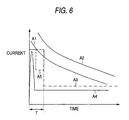
- Fig. 6 shows the heat-aging characteristic of an electric wire.
- the heat-aging characteristic indicates a conduction time taken for heat-aging of coating resin to begin to progress suddenly when a certain value of current is being applied to an electric wire.
- the heat-aging characteristic A1 at the time of one strand short-circuits is shifted to the lower current side than the heat-aging characteristic A2 in the condition of complete coating.
- the detection characteristic has a number of stages such as three-stage detection characteristic A5 shown by broken line in fig. 6.
- the present invention is intended to solve the forgoing problems, and it is an object thereof to provide an overcurrent detection circuit in which an overcurrent of a load in which a rush current may be generated can be detected suitably with a simple circuit configuration.
- an overcurrent detection circuit comprising: a switch means provided between a power supply and a load for switching connection on/off between the power supply and the load; a current detection means for detecting a load current flowing in the load; a reference value output means which outputs a reference value of a predetermined first level at the ON-time of the switch means and reduces the level of the reference value with passage of time from the ON-time so as to converge the level of the reference value to a predetermined second level; and an overcurrent signal output means which compares the detected load current with the reference value and outputs an overcurrent signal when the load current reaches or exceeds the reference value.
- the connection between the power supply and the load when the connection between the power supply and the load is turned on, a load current flowing in the load is detected, and the detected load current is compared with a reference value. If the load current becomes not smaller than the reference value, an overcurrent signal is outputted.
- the reference value is at a predetermined first level at the ON-time of the switch means. The level of the reference value is reduced with passage of time from the ON-time so as to be converged to a predetermined second level. As a result, an overcurrent in the load in which a rush current may be generated is detected suitably.
- the current detection means is constituted by a voltage converting circuit for converting the load current into a voltage of a level proportional to the load current; and the reference value output means is constituted by a reference voltage generating circuit for generating a reference voltage of the second level, and a charge/discharge circuit which outputs a charge voltage charged from the second level to the first level when the switch means is turned off, and which discharges the charged voltage at a predetermined time constant when the switch means is turned on.
- the reference voltage of the second level is generated.
- a charged voltage charged from the second level to the first level is outputted.
- the switch means is turned on, the charged voltage is discharged at a predetermined time constant.
- a voltage of the first level is outputted as the reference value at the ON-time of the switch means.
- the level of the voltage is reduced with passage of time from the ON-time so as to be converged to the second level.
- This reference value and the voltage of the level proportional to the load current are compared with each other, so that an overcurrent is detected properly.
- an overcurrent judgement means for making a judgment as to whether the overcurrent signal is outputted or not
- an overcurrent control means for turning the switch means off when the judgment proves that the overcurrent signal is outputted.
- the switch means is turned off in response to the conclusion that the overcurrent signal is outputted. Accordingly, the state of overcurrent is prevented from continuing.
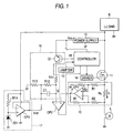
- Fig. 1 is a circuit diagram showing an embodiment of the overcurrent detection circuit according to the present invention.
- This embodiment is applied to a car lamp control circuit for controlling power supply from a battery (power supply) B to a lamp (load) L in a car.
- the lamp control circuit is constituted by an FET 11, a power supply circuit 12, a lamp switch 13, a driving circuit 14, a voltage converting circuit 15, a charge/discharge circuit 16, a reference voltage generating circuit 17, a control portion 18, a comparator OP2, and so on.
- the battery B is a power supply which outputs a constant voltage V B of about DC 12V.
- the power supply circuit 12 uses a not-shown three-terminal regulator so as to output a predetermined voltage V DD (DC 5V in this embodiment).
- the lamp switch 13 is operated from the outside so as to be turned on/off to thereby output an on/off signal which is an instruction to turn on/off the lamp L.
- the on/off signal is supplied to the control portion 18.
- the driving circuit 14 is constituted by a transistor, and so on, so as to apply a gate voltage to the FET 11 to turn the FET 11 on in response to a control signal supplied from the control portion 18.
- the voltage converting circuit 15 is constituted by an operational amplifier OP1, a shunt resistor Rs, and resistors R1, R2, R3 and Rf, and acts to convert a load current I L flowing in the lamp L into a voltage in proportion to the load current I L .
- the FET 11 and the shunt resistor Rs are connected in series between the battery B and the lamp L. More in detail, in the FET 11, the drain is connected to the positive pole of the battery B, the source is connected to one end of the shunt resistor Rs, and the gate is connected to the output terminal of the control portion 18 through the driving circuit 14. The other end of the shunt resistor Rs is grounded through an electric wire W and the lamp L. With such a configuration, electric power is supplied to the lamp L from the battery B through the shunt resistor Rs and the electric wire W when the FET 11 is turned on.
- the shunt resistor Rs is low in resistance and acts to detect the load current I L .
- the resistor R1 is connected at its one end to the one end of the shunt resistor Rs.
- the other end of the resistor R1 is connected to the not-inverted input terminal of the operational amplifier OP1, and, at the same time, grounded through the resistor R3.
- the resistor R2 is connected at its one end to the other end of the shunt resistor Rs.
- the other end of the resistor R2 is connected to the inverted input terminal of the operational amplifier OP1, and, at the same time, connected to the output terminal of the operational amplifier OP1 through the feedback resistor Rf.
- the output terminal (hereinafter referred to as "a point P") of the operational amplifier OP1 is connected to the not-inverted input terminal of the comparator OP2.
- the charge/discharge circuit 16 is constituted by resistors R11, R12 and R13, a capacitor C1 and a transistor Q1.
- the emitter is connected to the output terminal of the power supply circuit 12
- the base is connected to the output terminal of the control portion 18, and the collector is connected to the inverted input terminal (hereinafter referred to as "a point Q") of the comparator OP2 through the resistor R11.
- the output terminal of the comparator OP2 is connected to the input terminal of the control portion 18.
- One end of a parallel circuit constituted by the resistor 12 and the capacitor C1 is connected to the inverted input terminal of the comparator OP2, and the other end of this parallel circuit is connected to one end of the resistor R13.
- the other end of the resistor R13 is grounded.
- the reference voltage generating circuit 17 is constituted by an operational amplifier OP3, a resistor R14 and a Zener diode ZD1 so that the circuit 17 generates a reference voltage V ref (a reference voltage of a second level).
- the power supply terminal of the operational amplifier OP3 is connected to the positive pole of the battery B, and, at the same time, grounded through a series circuit constituted by the resistor R14 and the Zener diode ZD1.
- the output terminal is connected to the junction point between the resistors R12 and R13, the inverting input terminal is connected directly to the output terminal of the operational amplifier OP3, and the not-inverted input terminal is connected to the junction point between the resistor R14 and the Zener diode ZD1.
- the comparator OP2 has a function to act as an overcurrent signal output means. That is, the comparator OP2 compares the voltage V P at the point P which is proportional to the load current I L with the voltage V Q at the point Q as a reference value, and supplies a low-level signal to the control portion 18 when V P ⁇ V Q while it supplies an overcurrent signal of a high level to the control portion 18 when V P ⁇ V Q .
- the control portion 18 is constituted by a CPU, and so on, so as to control the operation of the lamp control circuit.
- the control portion 18 has functions (1) to (4) as follows.
- the shunt resistor Rs By using the shunt resistor Rs, not only the load current I L applied to the lamp L can be detected with high accuracy, but also a sudden change in current can be detected. In addition, if a resistor with low temperature dependency is used as the shunt resistor Rs, it is possible to improve the current detection accuracy against changes in the atmospheric temperature.
- the reference voltage generating circuit 17 is constituted by a so-called voltage follower circuit using an operational amplifier, it is possible to generate a constant reference voltage V ref independently of the current flowing in the resistors R12 and R13.
- This reference voltage V ref is set to a little higher level than the voltage V Pmax obtained by a maximum value I Lmax of the load current in the stationary state.
- the voltage V Q at the point Q at this time takes a value which is determined by the ratio of the resistor R11 to the resistor R12 and the reference voltage V ref .
- the FET 11 When the lamp switch 13 is turned on, the FET 11 is turned on. Accordingly, the lamp L is supplied with the load current I L and therefore turned on, while the transistor Q1 is turned off.
- V P I L ⁇ R S (R f /R 2 )
- R s designates a resistance value of the shunt resistor Rs
- R f designates a resistance value of the feedback resistor Rf
- R 2 designates a resistance value of the resistor R2.
- the resistance value of the resistor R1 is equal to that of the resistor R 2
- the resistance value of the resistor R3 is equal to that of the resistor R f .
- V Q V 0 ⁇ exp(-t/(R 12 C 1 )+V ref
- V 0 designates a voltage across the capacitor C1 charged fully
- R 12 designates a resistance value of the resistor R12
- C 1 designates a capacitance of the capacitor C1
- t designates an elapsed time since the transistor Q1 is turned on, that is, since the FET 11 is turned on.
- Fig. 2 is a graph showing an example of the change in voltage when a head lamp of 65 W is used as the lamp L
- Fig. 3 is a graph showing the change in current in the case of Fig. 2.
- I T designates a current at a level by which coating material of an electric wire of a single strand is aged by heat, that is, this current I T shows a heat-aging characteristic of a single strand.
- I Q designates a current on an overcurrent detection line according to this embodiment.
- V T designates a voltage appearing at the point P when the current I T flows in the shunt resistor Rs.
- an overcurrent detection line I Q larger than the normal load current I L and smaller than the current I T with the heat-aging characteristic of a single strand as shown in Fig. 3, without providing any complicated circuit such as a timer circuit, a multi-stage current detection circuit, or the like. Consequently, an overcurrent in a load such as the lamp L in which a rush current may be generated can be detected with accuracy by a simple-configuration circuit constituted by resistors, capacitors, operational amplifiers, etc.
- the voltage at a point P proportional to the load current I L of a lamp L is compared by a comparator OP2 with the voltage at a point Q as a reference value for overcurrent detection.
- the voltage obtained by adding the voltage charged in a capacitor C1 of a charge/discharge circuit 16 to the reference voltage V ref generated in a reference voltage generating circuit 17 is used as the reference value for overcurrent detection.
- the reference voltage generating circuit 17 is not limited to that shown in this embodiment, but may be configured as shown in Figs. 4 and 5. That is, Fig. 4 is a circuit diagram showing a modification of the reference voltage generating circuit 17.
- the reference voltage generating circuit 17 is constituted by an operational amplifier OP4, resistors R21 to R23, and transistors Q11 and Q12.
- the not-inverted input terminal of the operational amplifier OP4 is connected to its own output terminal through the resistor R21, and connected to the collector of the transistor Q11.
- the inverted input terminal of the reference voltage generating circuit 17 is connected to its own output terminal through the resistor R22, and connected to the collector of the transistor Q12 through the resistor R23.
- this circuit is designed such that the reference voltage V ref is outputted from the output terminal of the operational amplifier OP4.
- V R23 V BE1 - V BE2
- V R23 designates a voltage drop across the resistor R23
- V BE1 designates a base-to-emitter voltage of the transistor Q11
- V BE2 designates a base-to-emitter voltage of the transistor Q12.
- I E designates an emitter current
- I S designates a saturation current
- V BE designates a base-to-emitter voltage
- I C designates a collector current
- V R23 designates a voltage drop across the resistor R23
- I S1 designates a saturation current of the transistor Q11
- I S2 designates a saturation current of the transistor Q12.
- V ref V BE1 + V R21
- V ref V BE1 + (R 22 /R 23 )•V T •ln ⁇ (R 22 •I S2 )/(R 21 •I S1 ) ⁇
- V BE A - C• ⁇ T
- a and C designate constants respectively, and ⁇ T designates a change in temperature.
- Fig. 5 is a circuit diagram showing another modification of the reference voltage generating circuit 17.
- This reference voltage generating circuit 17 is constituted by a transistor Q21, resistors R31 to R33, diodes D1 to D3, and a Zener diode ZD2.
- the resistor R31, the diode D1 in the forward direction, and the Zener diode ZD2 in the reverse direction are connected in series to the output terminal of the power supply circuit 12 (see Fig. 1).
- the anode of the Zener diode ZD2 is grounded.
- the collector is connected to the output terminal of the power supply circuit 12 (see Fig. 1), the base is connected to the junction point between the resistor R31 and the diode D1, and the emitter is connected to the anode of the diode D2.
- the resistors R32 and R33, and the diode D3 in the forward direction are connected in series to the cathode of the diode D2.
- the cathode of the diode D3 is grounded.
- the reference voltage generating circuit 17 is designed so that the reference voltage V ref is outputted from the junction point between the resistors R32 and R33.
- V ref (V ZD +V D1 -V BE -V D2 -V D3 )•R 33 /(R 32 +R 33 ) + V D3
- V ZD designates the Zener voltage of the Zener diode ZD2
- V D1 , V D2 and V D3 designate the forward-direction voltages of the diodes D1, D2 and D3 respectively
- V BE designates the base-to-emitter voltage of the transistor Q21
- R 32 and R 33 designate the resistances of the resistors R32 and R33 respectively.
- a detected load current is compared with the reference value, and when the load current is larger than the reference value, an overcurrent signal is outputted. Accordingly, it is possible to suitably detect an overcurrent in the load in which a rush current may be generated.
- the reference voltage of the second level is generated.
- a charged voltage charged from the second level to the first level is outputted.
- the switch means is turned on, the charged voltage is discharged at a predetermined time constant.
- a voltage of the first level is outputted as the reference value at the ON-time of the switch means.
- the level of the voltage is reduced with passage of time from the ON-time so as to be converged to the second level.
- This reference value and the voltage of the level proportional to the load current are compared with each other, so that an overcurrent is detected properly.
- the switch means is turned off in response to the conclusion that the overcurrent signal is outputted. Accordingly, the state of overcurrent is prevented from continuing.
Description
Claims (4)
- An overcurrent detection circuit comprising:a switch means (11) provided between a power supply (12) and a load (L) for switching connection on/off between said power supply (12) and said load (L);a current detection means (15) for detecting a load current flowing in said load (L);a reference value output means (16, 17) which outputs at least a first reference value of a predetermined first level at the ON-time of said switch means (11) and a second reference value of a predetermined second level after passage of a time period; andan overcurrent signal output means (OP 2) which compares said detected load current with said reference values and outputs an overcurrent signal when said load current reaches or exceeds said second reference value, characterized in thata) said reference value output means (16, 17) is comprised of a single voltage generator circuit (17) having a single reference voltage output (Vef); andb) said reference value output means (16, 17) is formed for continuously reducing the level of said reference value with passage of time from said ON-time so as to converge the level of said reference value to said predetermined second level.
- An overcurrent detection circuit according to Claim1, wherein said current detection means (15) is constituted by a voltage converting circuit for converting said load current into a voltage of a level proportional to said load current; and
wherein said reference value output means (16, 17) is constituted by a reference voltage generating circuit (17) for generating a reference voltage of said second level, and a charge/discharge circuit (16) which outputs a charge voltage charged from said second level to said first level when said switch means (11) is turned off, and which discharges said charged voltage at a predetermined time constant when said switch means (11) is turned on. - An overcurrent detection circuit according to claim 1, further comprising an overcurrent judgement means (12) for making a judgment as to whether said overcurrent signal is outputted or not, and an overcurrent control means (within 18) for turning said switch means (11) off when said judgment proves that said overcurrent signal is outputted.
- An overcurrent detection circuit according to claim 2, further comprising an overcurrent judgement means (18) for making a judgment as to whether said overcurrent signal is outputted or not, and an overcurrent control means (within 18) for turning said switch means (11) off when said judgment proves that said overcurrent signal is outputted.
Applications Claiming Priority (3)
| Application Number | Priority Date | Filing Date | Title |
|---|---|---|---|
| JP215296/97 | 1997-08-08 | ||
| JP21529697A JP3363074B2 (en) | 1997-08-08 | 1997-08-08 | Overcurrent detection circuit |
| JP21529697 | 1997-08-08 |
Publications (3)
| Publication Number | Publication Date |
|---|---|
| EP0896410A2 EP0896410A2 (en) | 1999-02-10 |
| EP0896410A3 EP0896410A3 (en) | 2000-12-27 |
| EP0896410B1 true EP0896410B1 (en) | 2003-11-12 |
Family
ID=16669981
Family Applications (1)
| Application Number | Title | Priority Date | Filing Date |
|---|---|---|---|
| EP98114919A Expired - Lifetime EP0896410B1 (en) | 1997-08-08 | 1998-08-07 | Overcurrent detection circuit |
Country Status (4)
| Country | Link |
|---|---|
| US (1) | US6094092A (en) |
| EP (1) | EP0896410B1 (en) |
| JP (1) | JP3363074B2 (en) |
| DE (1) | DE69819625T2 (en) |
Families Citing this family (15)
| Publication number | Priority date | Publication date | Assignee | Title |
|---|---|---|---|---|
| DE10036983A1 (en) * | 2000-07-29 | 2002-02-14 | Bosch Gmbh Robert | Device for fast short-circuit protection in a power semiconductor |
| TWI245122B (en) * | 2001-06-29 | 2005-12-11 | Winbond Electronics Corp | Temperature measurement method and device with voltage variation compensation |
| US6680642B2 (en) * | 2002-05-23 | 2004-01-20 | Innersea Technology | Analog bipolar current source |
| JP2004080087A (en) * | 2002-08-09 | 2004-03-11 | Renesas Technology Corp | Overcurrent detecting circuit |
| JP4158754B2 (en) * | 2004-09-30 | 2008-10-01 | 日産自動車株式会社 | Overcurrent detection method and detection circuit |
| DE102004056868A1 (en) * | 2004-11-25 | 2006-06-01 | Hella Kgaa Hueck & Co. | Arrangement for detecting sparks and/or short circuits in circuit and interrupting circuit has current sensor and switching arrangement formed by semiconducting circuit |
| US20060228238A1 (en) * | 2005-04-06 | 2006-10-12 | Andrews Gregory C | Coolant pump for x-ray device |
| KR100780938B1 (en) * | 2005-06-03 | 2007-12-03 | 삼성전자주식회사 | Auto trimming bias voltage generator |
| US7675308B1 (en) * | 2008-08-20 | 2010-03-09 | Faraday Technology Corp. | Test circuit and test method for power switch |
| JP2010158109A (en) | 2008-12-26 | 2010-07-15 | Yazaki Corp | Load circuit protection device |
| JP2012032405A (en) * | 2011-11-02 | 2012-02-16 | Chugoku Electric Power Co Inc:The | Overheat diagnosis system and overheat diagnosis program |
| DE102014100830A1 (en) * | 2014-01-24 | 2015-07-30 | Murrelektronik Gmbh | Electrical fuse, decentralized fuse unit and system |
| JP6299740B2 (en) * | 2015-12-25 | 2018-03-28 | アンデン株式会社 | Overcurrent protection circuit |
| KR20170116472A (en) * | 2016-04-11 | 2017-10-19 | 주식회사 엘지화학 | Apparatus and method for protecting MOSFET relay using a voltage detector and signal fuse |
| CN115201554B (en) * | 2022-09-16 | 2023-01-13 | 中车工业研究院(青岛)有限公司 | No-load overcurrent detection circuit and no-load overcurrent detection system |
Family Cites Families (4)
| Publication number | Priority date | Publication date | Assignee | Title |
|---|---|---|---|---|
| JP2999887B2 (en) * | 1992-10-09 | 2000-01-17 | 三菱電機株式会社 | IGBT overcurrent protection circuit and semiconductor integrated circuit device |
| JPH0723525A (en) * | 1993-06-30 | 1995-01-24 | Nec Corp | Overcurrent detecting circuit |
| JP3053065B2 (en) * | 1995-04-05 | 2000-06-19 | 富士電気化学株式会社 | Overcurrent detection circuit |
| JP3384522B2 (en) * | 1996-07-30 | 2003-03-10 | 矢崎総業株式会社 | Switching device |
-
1997
- 1997-08-08 JP JP21529697A patent/JP3363074B2/en not_active Expired - Fee Related
-
1998
- 1998-08-05 US US09/129,609 patent/US6094092A/en not_active Expired - Lifetime
- 1998-08-07 DE DE69819625T patent/DE69819625T2/en not_active Expired - Lifetime
- 1998-08-07 EP EP98114919A patent/EP0896410B1/en not_active Expired - Lifetime
Also Published As
| Publication number | Publication date |
|---|---|
| US6094092A (en) | 2000-07-25 |
| DE69819625T2 (en) | 2004-08-19 |
| JP3363074B2 (en) | 2003-01-07 |
| JPH1151983A (en) | 1999-02-26 |
| EP0896410A2 (en) | 1999-02-10 |
| DE69819625D1 (en) | 2003-12-18 |
| EP0896410A3 (en) | 2000-12-27 |
Similar Documents
| Publication | Publication Date | Title |
|---|---|---|
| EP0896410B1 (en) | Overcurrent detection circuit | |
| US7443645B2 (en) | Overcurrent detecting device | |
| KR100691599B1 (en) | Overcurrent detection method and detection circuit | |
| US8760832B2 (en) | Load circuit protection device | |
| US8450982B2 (en) | Charge control circuit and charge controlling semiconductor integrated circuit | |
| US11031771B2 (en) | Power supply control apparatus | |
| US7061302B2 (en) | Semiconductor integrated circuit device | |
| JPH09224367A (en) | Switching control integrated circuit | |
| EP0793343B1 (en) | Current limitation programmable circuit for smart power actuators | |
| US20100020450A1 (en) | Power supply switching apparatus with severe overload detection | |
| EP0608974B1 (en) | Base current-control circuit of an output transistor | |
| EP0730331A3 (en) | Circuit for limiting switching overvoltages in power semiconductor switches | |
| JP2002017036A (en) | Over-current detection circuit | |
| US20080116859A1 (en) | Dropper type regulator | |
| JP4082547B2 (en) | Power supply control device for light emitting element | |
| US6337587B2 (en) | Circuit arrangement for driving a load by two transistors | |
| JP3713795B2 (en) | Output circuit of control device | |
| JP2000236245A (en) | Unit and method for power supply control | |
| US20050088239A1 (en) | Short-circuit detecting and protecting circuit for integrated circuit | |
| KR20010023993A (en) | Method and device for controlling an integrated power amplifier stage | |
| JPH08106331A (en) | Power source controller | |
| JPS6245486Y2 (en) | ||
| KR960012337B1 (en) | Electric discharge alarm circuit for a car | |
| KR200321222Y1 (en) | A device for preventing overcurrent | |
| KR940006855Y1 (en) | Voltage display circuit in a fire alarm receiver |
Legal Events
| Date | Code | Title | Description |
|---|---|---|---|
| PUAI | Public reference made under article 153(3) epc to a published international application that has entered the european phase |
Free format text: ORIGINAL CODE: 0009012 |
|
| AK | Designated contracting states |
Kind code of ref document: A2 Designated state(s): DE FR GB |
|
| AX | Request for extension of the european patent |
Free format text: AL;LT;LV;MK;RO;SI |
|
| PUAL | Search report despatched |
Free format text: ORIGINAL CODE: 0009013 |
|
| AK | Designated contracting states |
Kind code of ref document: A3 Designated state(s): AT BE CH CY DE DK ES FI FR GB GR IE IT LI LU MC NL PT SE |
|
| AX | Request for extension of the european patent |
Free format text: AL;LT;LV;MK;RO;SI |
|
| 17P | Request for examination filed |
Effective date: 20010206 |
|
| 17Q | First examination report despatched |
Effective date: 20010716 |
|
| AKX | Designation fees paid |
Free format text: DE FR GB |
|
| RAP1 | Party data changed (applicant data changed or rights of an application transferred) |
Owner name: SUMITOMO ELECTRIC INDUSTRIES, LTD. Owner name: AUTONETWORKS TECHNOLOGIES, LTD. Owner name: SUMITOMO WIRING SYSTEMS, LTD. |
|
| GRAH | Despatch of communication of intention to grant a patent |
Free format text: ORIGINAL CODE: EPIDOS IGRA |
|
| RIN1 | Information on inventor provided before grant (corrected) |
Inventor name: UMEDA, YUKIHIKOTOYOTA JIDOSHA KABUSHIKI KAISHA Inventor name: TABATA, YUKINOBUAUTONETWORKS TECHNOLOGIES, LTD. Inventor name: HOSHINO, TAKASHIAUTONETWORKS TECHNOLOGIES, LTD. Inventor name: MIZUNO, FUMIAKIAUTONETWORKS TECHNOLOGIES, LTD. |
|
| GRAS | Grant fee paid |
Free format text: ORIGINAL CODE: EPIDOSNIGR3 |
|
| GRAA | (expected) grant |
Free format text: ORIGINAL CODE: 0009210 |
|
| AK | Designated contracting states |
Kind code of ref document: B1 Designated state(s): DE FR GB |
|
| REG | Reference to a national code |
Ref country code: GB Ref legal event code: FG4D |
|
| REF | Corresponds to: |
Ref document number: 69819625 Country of ref document: DE Date of ref document: 20031218 Kind code of ref document: P |
|
| ET | Fr: translation filed | ||
| PG25 | Lapsed in a contracting state [announced via postgrant information from national office to epo] |
Ref country code: GB Free format text: LAPSE BECAUSE OF NON-PAYMENT OF DUE FEES Effective date: 20040807 |
|
| PLBE | No opposition filed within time limit |
Free format text: ORIGINAL CODE: 0009261 |
|
| STAA | Information on the status of an ep patent application or granted ep patent |
Free format text: STATUS: NO OPPOSITION FILED WITHIN TIME LIMIT |
|
| 26N | No opposition filed |
Effective date: 20040813 |
|
| GBPC | Gb: european patent ceased through non-payment of renewal fee |
Effective date: 20040807 |
|
| PGFP | Annual fee paid to national office [announced via postgrant information from national office to epo] |
Ref country code: DE Payment date: 20120731 Year of fee payment: 15 Ref country code: FR Payment date: 20120823 Year of fee payment: 15 |
|
| PG25 | Lapsed in a contracting state [announced via postgrant information from national office to epo] |
Ref country code: DE Free format text: LAPSE BECAUSE OF NON-PAYMENT OF DUE FEES Effective date: 20140301 |
|
| REG | Reference to a national code |
Ref country code: FR Ref legal event code: ST Effective date: 20140430 |
|
| REG | Reference to a national code |
Ref country code: DE Ref legal event code: R119 Ref document number: 69819625 Country of ref document: DE Effective date: 20140301 |
|
| PG25 | Lapsed in a contracting state [announced via postgrant information from national office to epo] |
Ref country code: FR Free format text: LAPSE BECAUSE OF NON-PAYMENT OF DUE FEES Effective date: 20130902 |