EP0894632B1 - Thermal head and method of its manufacture - Google Patents
Thermal head and method of its manufacture Download PDFInfo
- Publication number
- EP0894632B1 EP0894632B1 EP97949184A EP97949184A EP0894632B1 EP 0894632 B1 EP0894632 B1 EP 0894632B1 EP 97949184 A EP97949184 A EP 97949184A EP 97949184 A EP97949184 A EP 97949184A EP 0894632 B1 EP0894632 B1 EP 0894632B1
- Authority
- EP
- European Patent Office
- Prior art keywords
- thermal head
- layer
- section
- printing
- substrate
- Prior art date
- Legal status (The legal status is an assumption and is not a legal conclusion. Google has not performed a legal analysis and makes no representation as to the accuracy of the status listed.)
- Expired - Lifetime
Links
- 238000004519 manufacturing process Methods 0.000 title claims abstract description 117
- 238000000034 method Methods 0.000 title claims description 45
- 238000007639 printing Methods 0.000 claims abstract description 303
- 239000000758 substrate Substances 0.000 claims abstract description 148
- 229920005989 resin Polymers 0.000 claims abstract description 66
- 239000011347 resin Substances 0.000 claims abstract description 66
- 239000002390 adhesive tape Substances 0.000 claims abstract description 12
- 239000010410 layer Substances 0.000 claims description 590
- 238000005338 heat storage Methods 0.000 claims description 96
- 239000000126 substance Substances 0.000 claims description 40
- 229910052782 aluminium Inorganic materials 0.000 claims description 23
- 229920001721 polyimide Polymers 0.000 claims description 23
- 239000011521 glass Substances 0.000 claims description 22
- 239000004642 Polyimide Substances 0.000 claims description 21
- 239000000853 adhesive Substances 0.000 claims description 21
- PNEYBMLMFCGWSK-UHFFFAOYSA-N aluminium oxide Inorganic materials [O-2].[O-2].[O-2].[Al+3].[Al+3] PNEYBMLMFCGWSK-UHFFFAOYSA-N 0.000 claims description 20
- 229920001971 elastomer Polymers 0.000 claims description 20
- 239000012790 adhesive layer Substances 0.000 claims description 19
- 238000001039 wet etching Methods 0.000 claims description 19
- 229910052751 metal Inorganic materials 0.000 claims description 18
- 239000002184 metal Substances 0.000 claims description 18
- 230000001070 adhesive effect Effects 0.000 claims description 15
- 239000003822 epoxy resin Substances 0.000 claims description 13
- 229920000647 polyepoxide Polymers 0.000 claims description 13
- XAGFODPZIPBFFR-UHFFFAOYSA-N aluminium Chemical compound [Al] XAGFODPZIPBFFR-UHFFFAOYSA-N 0.000 claims description 12
- 229910052802 copper Inorganic materials 0.000 claims description 12
- 229920002050 silicone resin Polymers 0.000 claims description 11
- 229910004205 SiNX Inorganic materials 0.000 claims description 10
- 239000000919 ceramic Substances 0.000 claims description 10
- 229910052742 iron Inorganic materials 0.000 claims description 10
- 239000000203 mixture Substances 0.000 claims description 10
- 239000004925 Acrylic resin Substances 0.000 claims description 9
- 229920000178 Acrylic resin Polymers 0.000 claims description 9
- 238000000227 grinding Methods 0.000 claims description 9
- 229910052750 molybdenum Inorganic materials 0.000 claims description 8
- 229910052759 nickel Inorganic materials 0.000 claims description 8
- 239000000843 powder Substances 0.000 claims description 8
- 238000000151 deposition Methods 0.000 claims description 7
- 239000005388 borosilicate glass Substances 0.000 claims description 6
- 229920001187 thermosetting polymer Polymers 0.000 claims description 6
- 229910052721 tungsten Inorganic materials 0.000 claims description 6
- 239000013464 silicone adhesive Substances 0.000 claims description 5
- 239000004020 conductor Substances 0.000 claims description 3
- 230000003014 reinforcing effect Effects 0.000 claims description 3
- 230000008021 deposition Effects 0.000 claims description 2
- 239000012535 impurity Substances 0.000 claims description 2
- WFKWXMTUELFFGS-UHFFFAOYSA-N tungsten Chemical compound [W] WFKWXMTUELFFGS-UHFFFAOYSA-N 0.000 claims 1
- 239000010937 tungsten Substances 0.000 claims 1
- 238000005530 etching Methods 0.000 abstract description 35
- 238000010438 heat treatment Methods 0.000 abstract description 6
- 238000005299 abrasion Methods 0.000 abstract 2
- 230000005855 radiation Effects 0.000 abstract 2
- 230000001172 regenerating effect Effects 0.000 abstract 1
- VYPSYNLAJGMNEJ-UHFFFAOYSA-N Silicium dioxide Chemical compound O=[Si]=O VYPSYNLAJGMNEJ-UHFFFAOYSA-N 0.000 description 26
- 230000015572 biosynthetic process Effects 0.000 description 24
- 230000008569 process Effects 0.000 description 19
- 230000000694 effects Effects 0.000 description 18
- 239000000243 solution Substances 0.000 description 16
- 239000002131 composite material Substances 0.000 description 14
- 229910052814 silicon oxide Inorganic materials 0.000 description 14
- 239000010949 copper Substances 0.000 description 13
- 229910052681 coesite Inorganic materials 0.000 description 12
- 229910052906 cristobalite Inorganic materials 0.000 description 12
- 239000000377 silicon dioxide Substances 0.000 description 12
- 229910052682 stishovite Inorganic materials 0.000 description 12
- 229910052905 tridymite Inorganic materials 0.000 description 12
- 238000002844 melting Methods 0.000 description 10
- 230000008018 melting Effects 0.000 description 10
- 239000000463 material Substances 0.000 description 9
- 238000005268 plasma chemical vapour deposition Methods 0.000 description 9
- 238000004544 sputter deposition Methods 0.000 description 9
- 230000017525 heat dissipation Effects 0.000 description 8
- 239000010935 stainless steel Substances 0.000 description 8
- 229910001220 stainless steel Inorganic materials 0.000 description 8
- 238000007796 conventional method Methods 0.000 description 7
- 230000003247 decreasing effect Effects 0.000 description 7
- 150000001875 compounds Chemical class 0.000 description 6
- 230000007547 defect Effects 0.000 description 6
- 238000000926 separation method Methods 0.000 description 6
- 230000015556 catabolic process Effects 0.000 description 5
- 238000006731 degradation reaction Methods 0.000 description 5
- 230000000994 depressogenic effect Effects 0.000 description 5
- 238000001312 dry etching Methods 0.000 description 5
- 238000000206 photolithography Methods 0.000 description 5
- 238000001020 plasma etching Methods 0.000 description 5
- 229920001342 Bakelite® Polymers 0.000 description 4
- 239000004637 bakelite Substances 0.000 description 4
- 238000001816 cooling Methods 0.000 description 4
- 238000004518 low pressure chemical vapour deposition Methods 0.000 description 4
- 229920002120 photoresistant polymer Polymers 0.000 description 4
- 238000012545 processing Methods 0.000 description 4
- 229910000679 solder Inorganic materials 0.000 description 4
- 101000623895 Bos taurus Mucin-15 Proteins 0.000 description 3
- GRYLNZFGIOXLOG-UHFFFAOYSA-N Nitric acid Chemical compound O[N+]([O-])=O GRYLNZFGIOXLOG-UHFFFAOYSA-N 0.000 description 3
- 229910018487 Ni—Cr Inorganic materials 0.000 description 3
- NBIIXXVUZAFLBC-UHFFFAOYSA-N Phosphoric acid Chemical compound OP(O)(O)=O NBIIXXVUZAFLBC-UHFFFAOYSA-N 0.000 description 3
- 229910020286 SiOxNy Inorganic materials 0.000 description 3
- 229910045601 alloy Inorganic materials 0.000 description 3
- 239000000956 alloy Substances 0.000 description 3
- 238000009792 diffusion process Methods 0.000 description 3
- 239000000945 filler Substances 0.000 description 3
- 229910017604 nitric acid Inorganic materials 0.000 description 3
- 238000002294 plasma sputter deposition Methods 0.000 description 3
- 230000002787 reinforcement Effects 0.000 description 3
- 238000007650 screen-printing Methods 0.000 description 3
- 229910000881 Cu alloy Inorganic materials 0.000 description 2
- 229910000640 Fe alloy Inorganic materials 0.000 description 2
- XPDWGBQVDMORPB-UHFFFAOYSA-N Fluoroform Chemical compound FC(F)F XPDWGBQVDMORPB-UHFFFAOYSA-N 0.000 description 2
- -1 SiC compound Chemical class 0.000 description 2
- 239000003929 acidic solution Substances 0.000 description 2
- 230000008859 change Effects 0.000 description 2
- 238000005229 chemical vapour deposition Methods 0.000 description 2
- 238000004040 coloring Methods 0.000 description 2
- WABPQHHGFIMREM-UHFFFAOYSA-N lead(0) Chemical compound [Pb] WABPQHHGFIMREM-UHFFFAOYSA-N 0.000 description 2
- 230000000116 mitigating effect Effects 0.000 description 2
- 239000002245 particle Substances 0.000 description 2
- 238000007747 plating Methods 0.000 description 2
- 239000009719 polyimide resin Substances 0.000 description 2
- 238000002203 pretreatment Methods 0.000 description 2
- 230000001681 protective effect Effects 0.000 description 2
- 238000005476 soldering Methods 0.000 description 2
- 229910052715 tantalum Inorganic materials 0.000 description 2
- RYGMFSIKBFXOCR-UHFFFAOYSA-N Copper Chemical compound [Cu] RYGMFSIKBFXOCR-UHFFFAOYSA-N 0.000 description 1
- CTQNGGLPUBDAKN-UHFFFAOYSA-N O-Xylene Chemical compound CC1=CC=CC=C1C CTQNGGLPUBDAKN-UHFFFAOYSA-N 0.000 description 1
- 229910052581 Si3N4 Inorganic materials 0.000 description 1
- QAOWNCQODCNURD-UHFFFAOYSA-N Sulfuric acid Chemical compound OS(O)(=O)=O QAOWNCQODCNURD-UHFFFAOYSA-N 0.000 description 1
- 239000002253 acid Substances 0.000 description 1
- 239000004840 adhesive resin Substances 0.000 description 1
- 229920006223 adhesive resin Polymers 0.000 description 1
- LDDQLRUQCUTJBB-UHFFFAOYSA-N ammonium fluoride Chemical compound [NH4+].[F-] LDDQLRUQCUTJBB-UHFFFAOYSA-N 0.000 description 1
- 229910052788 barium Inorganic materials 0.000 description 1
- DSAJWYNOEDNPEQ-UHFFFAOYSA-N barium atom Chemical compound [Ba] DSAJWYNOEDNPEQ-UHFFFAOYSA-N 0.000 description 1
- 230000005540 biological transmission Effects 0.000 description 1
- 238000010276 construction Methods 0.000 description 1
- PMHQVHHXPFUNSP-UHFFFAOYSA-M copper(1+);methylsulfanylmethane;bromide Chemical compound Br[Cu].CSC PMHQVHHXPFUNSP-UHFFFAOYSA-M 0.000 description 1
- 229910052593 corundum Inorganic materials 0.000 description 1
- 238000010586 diagram Methods 0.000 description 1
- 230000003292 diminished effect Effects 0.000 description 1
- 239000000428 dust Substances 0.000 description 1
- 238000009713 electroplating Methods 0.000 description 1
- 238000011156 evaluation Methods 0.000 description 1
- SLGWESQGEUXWJQ-UHFFFAOYSA-N formaldehyde;phenol Chemical compound O=C.OC1=CC=CC=C1 SLGWESQGEUXWJQ-UHFFFAOYSA-N 0.000 description 1
- 229910052737 gold Inorganic materials 0.000 description 1
- 230000020169 heat generation Effects 0.000 description 1
- 238000011835 investigation Methods 0.000 description 1
- 229910052749 magnesium Inorganic materials 0.000 description 1
- 150000002739 metals Chemical class 0.000 description 1
- 239000011259 mixed solution Substances 0.000 description 1
- 230000036961 partial effect Effects 0.000 description 1
- 229920001568 phenolic resin Polymers 0.000 description 1
- 238000000623 plasma-assisted chemical vapour deposition Methods 0.000 description 1
- 229920003229 poly(methyl methacrylate) Polymers 0.000 description 1
- 229910021420 polycrystalline silicon Inorganic materials 0.000 description 1
- 239000004926 polymethyl methacrylate Substances 0.000 description 1
- 230000002829 reductive effect Effects 0.000 description 1
- 238000012827 research and development Methods 0.000 description 1
- 230000000717 retained effect Effects 0.000 description 1
- 230000002441 reversible effect Effects 0.000 description 1
- 239000004065 semiconductor Substances 0.000 description 1
- 238000004904 shortening Methods 0.000 description 1
- 239000002904 solvent Substances 0.000 description 1
- 238000012360 testing method Methods 0.000 description 1
- 229910052718 tin Inorganic materials 0.000 description 1
- 229910052719 titanium Inorganic materials 0.000 description 1
- 238000012546 transfer Methods 0.000 description 1
- 230000007704 transition Effects 0.000 description 1
- 239000008096 xylene Substances 0.000 description 1
- 229910001845 yogo sapphire Inorganic materials 0.000 description 1
- 229910052726 zirconium Inorganic materials 0.000 description 1
Images

















Classifications
-
- B—PERFORMING OPERATIONS; TRANSPORTING
- B41—PRINTING; LINING MACHINES; TYPEWRITERS; STAMPS
- B41J—TYPEWRITERS; SELECTIVE PRINTING MECHANISMS, i.e. MECHANISMS PRINTING OTHERWISE THAN FROM A FORME; CORRECTION OF TYPOGRAPHICAL ERRORS
- B41J2/00—Typewriters or selective printing mechanisms characterised by the printing or marking process for which they are designed
- B41J2/315—Typewriters or selective printing mechanisms characterised by the printing or marking process for which they are designed characterised by selective application of heat to a heat sensitive printing or impression-transfer material
- B41J2/32—Typewriters or selective printing mechanisms characterised by the printing or marking process for which they are designed characterised by selective application of heat to a heat sensitive printing or impression-transfer material using thermal heads
- B41J2/335—Structure of thermal heads
- B41J2/33505—Constructional details
- B41J2/3352—Integrated circuits
-
- B—PERFORMING OPERATIONS; TRANSPORTING
- B41—PRINTING; LINING MACHINES; TYPEWRITERS; STAMPS
- B41J—TYPEWRITERS; SELECTIVE PRINTING MECHANISMS, i.e. MECHANISMS PRINTING OTHERWISE THAN FROM A FORME; CORRECTION OF TYPOGRAPHICAL ERRORS
- B41J2/00—Typewriters or selective printing mechanisms characterised by the printing or marking process for which they are designed
- B41J2/315—Typewriters or selective printing mechanisms characterised by the printing or marking process for which they are designed characterised by selective application of heat to a heat sensitive printing or impression-transfer material
- B41J2/32—Typewriters or selective printing mechanisms characterised by the printing or marking process for which they are designed characterised by selective application of heat to a heat sensitive printing or impression-transfer material using thermal heads
- B41J2/335—Structure of thermal heads
- B41J2/3355—Structure of thermal heads characterised by materials
-
- B—PERFORMING OPERATIONS; TRANSPORTING
- B41—PRINTING; LINING MACHINES; TYPEWRITERS; STAMPS
- B41J—TYPEWRITERS; SELECTIVE PRINTING MECHANISMS, i.e. MECHANISMS PRINTING OTHERWISE THAN FROM A FORME; CORRECTION OF TYPOGRAPHICAL ERRORS
- B41J2/00—Typewriters or selective printing mechanisms characterised by the printing or marking process for which they are designed
- B41J2/315—Typewriters or selective printing mechanisms characterised by the printing or marking process for which they are designed characterised by selective application of heat to a heat sensitive printing or impression-transfer material
- B41J2/32—Typewriters or selective printing mechanisms characterised by the printing or marking process for which they are designed characterised by selective application of heat to a heat sensitive printing or impression-transfer material using thermal heads
- B41J2/335—Structure of thermal heads
- B41J2/33555—Structure of thermal heads characterised by type
- B41J2/3357—Surface type resistors
-
- B—PERFORMING OPERATIONS; TRANSPORTING
- B41—PRINTING; LINING MACHINES; TYPEWRITERS; STAMPS
- B41J—TYPEWRITERS; SELECTIVE PRINTING MECHANISMS, i.e. MECHANISMS PRINTING OTHERWISE THAN FROM A FORME; CORRECTION OF TYPOGRAPHICAL ERRORS
- B41J2/00—Typewriters or selective printing mechanisms characterised by the printing or marking process for which they are designed
- B41J2/315—Typewriters or selective printing mechanisms characterised by the printing or marking process for which they are designed characterised by selective application of heat to a heat sensitive printing or impression-transfer material
- B41J2/32—Typewriters or selective printing mechanisms characterised by the printing or marking process for which they are designed characterised by selective application of heat to a heat sensitive printing or impression-transfer material using thermal heads
- B41J2/335—Structure of thermal heads
- B41J2/33575—Processes for assembling process heads
-
- B—PERFORMING OPERATIONS; TRANSPORTING
- B41—PRINTING; LINING MACHINES; TYPEWRITERS; STAMPS
- B41J—TYPEWRITERS; SELECTIVE PRINTING MECHANISMS, i.e. MECHANISMS PRINTING OTHERWISE THAN FROM A FORME; CORRECTION OF TYPOGRAPHICAL ERRORS
- B41J2/00—Typewriters or selective printing mechanisms characterised by the printing or marking process for which they are designed
- B41J2/315—Typewriters or selective printing mechanisms characterised by the printing or marking process for which they are designed characterised by selective application of heat to a heat sensitive printing or impression-transfer material
- B41J2/32—Typewriters or selective printing mechanisms characterised by the printing or marking process for which they are designed characterised by selective application of heat to a heat sensitive printing or impression-transfer material using thermal heads
- B41J2/335—Structure of thermal heads
- B41J2/3359—Manufacturing processes
-
- Y—GENERAL TAGGING OF NEW TECHNOLOGICAL DEVELOPMENTS; GENERAL TAGGING OF CROSS-SECTIONAL TECHNOLOGIES SPANNING OVER SEVERAL SECTIONS OF THE IPC; TECHNICAL SUBJECTS COVERED BY FORMER USPC CROSS-REFERENCE ART COLLECTIONS [XRACs] AND DIGESTS
- Y10—TECHNICAL SUBJECTS COVERED BY FORMER USPC
- Y10T—TECHNICAL SUBJECTS COVERED BY FORMER US CLASSIFICATION
- Y10T29/00—Metal working
- Y10T29/49—Method of mechanical manufacture
- Y10T29/49002—Electrical device making
- Y10T29/49082—Resistor making
- Y10T29/49083—Heater type
Definitions
- This invention relates to a thermal head for use in a thermo-recording machine such as printer and facsimile and a method of manufacturing the same, and more particularly to a thermal head comprising a printing section including a wear-resistant layer having a printing surface to be brought into contact with a thermal record medium, a heat generating layer for generating heat to be transmitted to the thermal record medium through the wear-resistant layer and an electrically conductive layer connected to the heat generating layer, a driving circuit section connected to the electrically conductive layer of the printing section to control a heating electric power to be supplied to the printing section, and a wiring section for connecting the driving circuit section to an external circuit and a method of manufacturing such a thermal head.
- a thermal head is an equipment, in which heat generated in accordance with a supplied electric signal is transmitted to a thermal record medium, for instance a thermal paper to record characters and figures of desired shapes.
- a conventional thermal head is composed of the following basic components:
- a printing section includes a printing surface to be brought into contact with a thermal paper and generates and transmits heat for coloring the thermal paper.
- a driving circuit section supplies an electric power according to an electric signal bearing information to be printed.
- the information is to be understood to mean image data representing characters and figures. Since normal semiconductor integrated circuit chips are used as the driving circuit, the driving circuit is denoted as a driving IC for the sake of simplicity in the present specification.
- a wiring section is provided for connecting the thermal head to a connector of a cable to be connected to an external circuit.
- the printing information and electric power are supplied to the thermal head from the external circuit via the wiring section.
- a connection to the external circuit is performed by a lead wire such as a flexible FPC (Flexible Print Circuit), and in this case, the wiring section includes pin-like conductors to be connected to the connector of the lead wire, a part of said pin-like conductors being exposed from the thermal head.
- Fig. 1 is a cross sectional view showing a structure of an example of the conventional thermal head, in which a driving IC is connected to a printing section and a wiring section by means of wire-bonding.
- the thermal head shown in Fig. 1 has been used in a usual type thermo-recording printer.
- Fig. 1 In Fig. 1.
- a reference numeral 10 denotes a wear-resistant layer having anti-physical and anti-chemical characters
- a reference numeral 11 a heat generating layer
- reference numerals 12a and 12b an electrically conductive layer constituting electrodes for the heat generating layer
- a reference numeral 13 an electrically conductive layer constituting a wiring section for connecting the thermal head to an external circuit
- a reference numeral 14 solders constituting connecting portions for connecting the wiring section and a wiring cable with each other
- a reference numeral 15 a driving IC a reference numeral 16 a wiring for connecting the driving to the external circuit
- a reference numeral 17 a heat storage layer
- a reference numeral 18 a resin layer for isolating and protecting the driving IC and bonding wires
- a reference numeral 19 an electrically insulating substrate
- a reference numeral 20 bonding wires connecting terminals of the driving IC to the electrically conductive layer 12b and wiring section
- a reference numeral 21 a thermal paper
- a reference character P shows a printing section which is composed of a part of the wear-resistant layer 10, the heat generating layer 11 and parts of the electrically conductive layers 12a and 12b.
- a reference character S denotes the printing surface of the printing section P, that is a part of the surface of the wear-resistant layer 10 which is brought into contact with the thermal paper 21.
- a reference character L expresses a distance between the printing section P and the resin layer 18 protecting the driving IC 15.
- the heat storage layer 17 is formed on the substrate 19, on which the heat generating layer 11, electrically conductive layers 12a and 12b and wear-resistant layer 10 constituting the printing section P are successively stacked.
- the thermal head shown in Fig. 1 will be further explained by dividing it into several components.
- the conventional thermal head illustrated in Fig. 1 is composed not only of the basic components (Component I), (Component II), and (Component III), but also by the heat storage layer of (Component IV). These components are arranged on the substrate 19 of (Component V). In other words, the (Component I)-(Component IV) are supported as a unit body by means of the (Component V).
- thermal heads in which a heat radiating or other components for increasing a printing speed. By providing such a component, a performance of the thermal head can be improved.
- the heat generating layer 11 constituting the printing section P is divided into many heat generating elements in a direction normal to a plane of the drawing of Fig. 1.
- the electrically conductive layer 12a form a common electrodes to these heat generating elements and the electrically conductive layer 12b constitutes divided electrodes each being connected to respective heat generating elements in order to flow an electric current only through one or more desired heat generating elements according to the print information.
- the common electrode and divided electrodes are called the electrically conductive layer in a general term in this specification.
- the wear-resistant layer 10 is brought into contact with the thermal paper 21 to transmit the heat generated by the heat generating layer 11 to the thermal paper. Therefore the printing surface S is composed of the surface of the wear-resistant layer 10 situating in the printing section P.
- the wear-resistant layer 10 is required to have a basic characteristic that the layer does not chemically react to components contained in the thermal paper. Moreover good wear-resistant and heat-resistant characteristics, a lower coefficient of friction and a proper hardness are required for the wear-resistant layer. Furthermore, the wear-resistant layer preferably has a suitable electrical conductivity.
- the wear-resistant layer preferably has a proper electric conductivity. However since an extended portion of the wear-resistant layer extending from the printing section P is brought into contact with respective electrodes of the electrically conductive layer 12b, the wear-resistant layer should have such a resistance that these electrodes are not short-circuited.
- the heat generating layer 11 has a function of generating heat for coloring the thermal paper.
- the principle of the heat generation is based on the Joule heat, wherein heat is generated by flowing an electric current through a resistive body. Accordingly the heat generating layer 11 is required to have a stable electric property around 400°C.
- the electric property mainly means a resistance and its change with time.
- the electrically conductive layers 12a and 12b are used to establish an electrical connection within the thermal head.
- the electrically conductive layer 12a constitutes the common electrode which commonly connects one ends of respective heat generating elements of the heat generating layer 11 to, for instance the ground potential point.
- the electrically conductive layer 12b constitutes many electrodes for connecting respective heat generating elements of the heat generating layer 11 to the driving IC 15 separately. To this end, bonding wires 20 are soldered to the electrically conductive layer 12b and driving IC 15.
- the electrically conductive layers 12a and 12b are contacted with the heat generating layer 11, the electrically conductive layers are influenced by the heat of about 400°C generated during the printing operation. In a process of manufacturing the thermal head, the layers are heated to about 350°C during the formation of the wear-resistant layer 10. Consequently the conductive layers 12a and 12b are also required to have a stable electric property at around 400C.
- the electric property mainly means a resistance and its change with time.
- the electrically conductive layer 13 constituting the wiring section is soldered to the driving IC 15 and bonding wires 20, and is also connected to wires, for instance the pins 16 by solders 14 for establishing a connection to the external circuit.
- the heat storage layer 17 has a function for holding the heat generated by the heat generating layer 11 for a certain time period and preventing the heat from being transmitted to the driving IC 15 through the resin layer 18.
- the heat storage layer 17 should have a low thermal conductivity and a high heat-resistance.
- the substrate 19 constitutes fundamentally a supporting body of the thermal head. That is to say, the substrate has a function for supporting the printing section P, driving IC 15, electrically conductive layer 13 constituting the wiring section for connecting the thermal head to the external circuit, wires 16 connected to the wiring section.
- the substrate may be heated to about 400°C during the manufacturing process.
- the substrate 19 should have a high mechanical strength as well as a high heat-resistance.
- the substrate preferably has a high thermal conductivity such that the heat generated by the thermal head during the printing operation could be dissipated.
- the resin layer 18 is used to protect the driving IC 15 and the bonding wire 20, and thus the resin layer should have a proper mechanical strength and a certain electrically insulating property.
- the wear-resistant layer 10 is preferably made of a substance which satisfies all the desired conditions mentioned above, such a substance could hardly be found.
- SiC based compound, SiB based compound, SiO based compound and SiON based compound may be listed as a substance which can satisfy the conditions to a relatively large extent.
- the heat generating layer 11 has to be made of a substance which reveals a stable electric property at about 400°C.
- the heat generating layer is made of a metal such as Ta, an alloy such as Ni-Cr, a poly-Si and a mixture of a transition element and SiO 2 such as Nb-SiO 2 .
- a metal such as Ta
- an alloy such as Ni-Cr
- a poly-Si a mixture of a transition element and SiO 2
- SiO 2 such as Nb-SiO 2 .
- Nb-SiO 2 has been generally used, because its resistance can be easily controlled.
- the electrically conductive layer 12a, 12b and wiring section 13 should be made of a substance also having a stable electric property at about 400°C. W, Ta, Au, Al and the like may be listed as such a substance.
- the heat storage layer 17 has to be made of a substance having a small thermal conductivity as well as a high heat-resistant property.
- Bakelite, polyimide, glass and the like may be listed as such a substance.
- the Bakelite is a trade name of phenol-formaldehyde. Glass has been generally used due to its hardness.
- the substrate 19 should be made of a substance having a high thermal conductivity and a high heat-resistance.
- MgO, ZnO, aluminum nitride, alumina ceramics and the like may be listed for such a substance.
- the alumina ceramics have been generally used due to its easy processing and low cost.
- the printing in the thermal head is carried out by conducting the heat generated by the heat generating layer 11 to the thermal paper 21 through the wear-resistant layer 10. Accordingly, in order to achieve a clear printing, the heat generated by the heat generating layer 11 has to be efficiently transmitted to the thermal paper 21.
- a method of making a tight contact between the printing surface S and the thermal paper 21 will be described while a facsimile is taken as an example.
- the thermal paper 21 is generally urged against the printing surface S of the printing section P by means of the rubber roller 22.
- the rubber roller 22 also serves as a paper feeder. Accordingly upon designing the rubber roller 22, the hardness and shape of the rubber roller 22 are determined such that the tight contact can be attained between the printing surface S and the thermal paper 21 as far as possible.
- Figs. 1-3 are cross sectional views showing the structure of known thermal heads.
- the driving IC 15 is connected by means of the wire-bonding, and particularly the thermal head illustrated in Fig. 2 has the printing section which is higher than that of the thermal head shown in Fig. 1.
- the driving IC is connected by means of the flip chip bonding.
- Portions of the thermal heads shown in Figs. 2 and 3 similar to those of Fig. 1 are denoted by the same reference numerals used in Fig. 1. It should be noted that in Fig.
- a reference character I denotes a height from the surface of the substrate 19 to the printing section S
- a reference character H a height from the surface of the substrate to a top of a bonding wire loop
- a reference character X represents a depressed portion of the printing section.
- the driving IC 15 has been connected to the electrically conductive layer 12b and electrically conductive layers of the wiring section 13 by means of the following methods.
- a metal wire called a bonding wire is fused to the terminals of the driving IC as well as to an electrically conductive layer at a predetermined position.
- the wire bonding has been widely used as the connection method for the driving IC.
- the wire-bonding is described in, for instance Japanese Patent Application Publication No. 6-78004.
- Figs. 1 and 2 show the driving IC 15 connected by a bonding wire 20.
- the flip chip bonding is a connecting method, in which solder balls are formed on a lower surface of the driving IC to be connected and the balls are fused to the conductive layer.
- the method is described in, for instance "Oki Electric Research and Development", No. 138, Vol. 55, No. 2.
- Fig. 3 illustrates the driving IC 15 connected by the flip chip bonding.
- TAB Tape Automated Bonding.
- the tape is a connecting part formed by covering plural metal wires with an insulating resin and both ends of the metal wires are exposed on both ends.
- the terminals of the driving IC are simultaneously connected to the electrically conductive layers at predetermined positions.
- Fig. 1 shows the driving IC connected by the wire bonding.
- the driving IC 15 and the printing section P when a distance between the driving IC 15 and the printing section P is small, the following defects might occur.
- the distance L has to be at least about 10 mm, so that the thermal head could not be further miniaturized.
- the height I of the printing surface S measured from the surface of the substrate 19 has to be not less than 200 ⁇ m. Now methods of making the height I of the printing surface S larger will be explained.
- the heat storage layer 17 is formed on the substrate 19 such that its thickness is partially increased, and the printing surface S is formed on the heat storage layer such that the printing surface is protruded outwardly. Since the height H of a top of a loop of the bonding wires 20 is about 200 ⁇ m, the above problem could not be solved as long as the height I of the printing section P is not less than 200 ⁇ m. However, an actual height I of the printing surface S is about 50 ⁇ m.
- the height I of the printing surface S is made not less than 200 ⁇ m, surfaces of the heat generating layer 11 and electrically conductive layers 12a, 12b are also protruded outwardly, and therefore etching processes by a photolithography could not be performed accurately and a precision of pattern dimension might be decreased. Therefore, the electric characteristics are liable to fluctuate.
- the depressed portion X is formed at a center of the printing surface S as shown in Fig. 2. Accordingly a tight contact could not be attained between the printing surface S and the thermal paper 21, and thus a print density might be reduced.
- the driving IC 15 is electrically connected by the flip chip bonding, after the driving IC is directly bonded to the conductive layer 12b and wiring section 13, the driving IC 15 is sealed with the resin 18. Therefore, the resin 18 might be brought into contact with the thermal paper 21 and rubber roller 22.
- the distance L between the driving IC and the printing section P has to be at least about 8 mm. Then, the thermal head could not be further miniaturized like as the above mentioned wire bonding.
- a method of manufacturing the thermal head as shown in Fig. 4 is described in Japanese Patent Application Laid-open Publication No. 5-64905.
- a stainless steel plate is used as a provisional substrate 30 for manufacturing the thermal head as shown in Fig. 4 and after grinding the surface of the stainless steel plate as a mirror surface, a peeling-off layer 31 is formed by electroplating of copper, on which the wear-resistant layer 10, the heat generating layer 11, and the conductive layers 12a and 12b are deposited in turn as shown in Fig. 4B ⁇ 4D and a heat storage layer 32 made of a heat-resist resin is formed as shown in Fig. 4E.
- an alumina substrate 34 is adhered on the heat storage layer 32 with an adhesive 33 as shown in Fig. 4F, and thereafter the provisional substrate 30 is peeled off at the interface of the peeled-off layer 31 to expose the wear-resistant layer 10 as a printing surface. Moreover a part of the wear-resistant layer 10 remote from the printing surface is removed to expose a part of the conductive layer 12b, to which the driving IC is connected to complete the thermal head.
- This conventional method of manufacturing the thermal head has the following problems.
- the thermal head has to be large to a certain extent and the printing section has to be projected largely.
- US 4841120 discloses a thermal head having a heat generating resistor and a driving circuit both formed on one side of a substrate, and a thermal recording face formed on the other side of the substrate.
- the thermal recording farce is formed by grinding the substrate.
- the present invention has for its object to provide a thermal head, in which although a size of the thermal head is made small, a driving IC and its electric connection parts are not brought into contact with a thermal paper and a rubber roller, and thus the electric equipment could be protected against the cutting-off and short-circuit and as a result of which, the manufacturing could be performed efficiently at a low-cost.
- a thermal head comprising: a printing section including a wear-resistant layer having a first surface constituting a printing face to be brought into contact with a thermal record medium and a second surface opposite to the first surface, a heat generating layer formed on a side of the second surface of the wear-resistant layer and generating heat to be transmitted to the thermal record medium through the wear-resistant layer, and an electrically conductive layer formed on the same side of the wear-resistant layer as the second surface and connected electrically to the heat generating layer; a driving circuit section connected to the electrically conductive layer of the printing section to control a heat generating electric power to be supplied to said printing section, said driving circuit section being arranged on the same side of the wear-resistant layer as the second surface; and a wiring section for connecting the driving circuit section to an external circuit, said wiring section being arranged on the same side of the wear-resistant layer as the second surface, characterized in that the printing surface of the printing section is formed as an outwardly protruding curved surface
- the driving circuit section and wiring section are arranged on a side of the wear-resistant layer opposite to the side which is to be brought into contact with a thermal record medium, the driving circuit section and connecting wires could not be brought into contact with the thermal record medium and rubber roller, and therefore a distance between the printing section and the driving circuit section can be shortened and the thermal head can be miniaturized.
- the thermal head Upon practicing the thermal head according to the invention, the thermal head can be classified into the following four groups in accordance with its principal structure.
- said wear-resistant layer in the printing section has an extended part which extends beyond the printing section
- said electrically conductive layer has an extended part which extends on a side of the second surface of the wear-resistant layer
- said wiring section is provided on a side of the second surface of the extended part of the wear-resistant layer
- said driving circuit part is composed of integrated circuit chips, terminals of which are connected electrically to the extended part of the electrically conductive layer and to the wiring section.
- the thermal head comprises a supporting member provided on a side of the second surface of the wear-resistant layer of the printing section for supporting the printing section, driving circuit section, and wiring section.
- Said supporting member may comprise a resin member for bonding and fixing the printing section, driving circuit section and wiring section integrally, and said resin member may be preferably made of epoxy resin, acrylic resin, or silicone resin.
- said supporting member comprises a heat dissipating member and an adhesive layer for fixing at least said printing section to said heat dissipating member.
- said supporting member comprises a flat plate and an adhesive layer for fixing at least said printing section to the flat plate.
- said printing surface may be flat or may be protruded outwardly.
- said adhesive is preferably made of a resin selected from the group of epoxy resin, acrylic resin and silicone resin. Furthermore, said adhesive resin may contain powders such as alumina powders for increasing a thermal conductivity. Moreover, in the third and fourth principal structures, said means for fixing the driving circuit section and a part of the wiring section to said heat dissipating layer or flat plate may be preferably formed in the supporting member. This fixing member may be advantageously formed by double-sided adhesive tape.
- said adhesive layer is preferably made of thermosetting adhesive agent, heat-resistant inorganic adhesive agent or viscoelastic rubber.
- said printing section may be constructed by stacking the wear-resistant layer, heat generating layer and electrically conductive layer or by stacking the wear-resistant layer, electrically conductive layer and heat generating layer in this order viewed from the printing surface.
- said printing section may comprise a protection layer on a side of the heat generating layer opposite to the printing surface, said protection layer preventing a diffusion of impurities into the heat generating layer.
- Said protection layer may be preferably made of at least one of SiNx and SiNx or a mixture thereof.
- said printing section may include a heat storage layer thermally coupled with the heat generating layer through the protection layer.
- Said heat storage layer may contain at least one of polyimide and glass.
- the heat storage layer may be preferably made of a polyimide containing powders for adjusting its thermal conductivity.
- the thermal head according to the invention may further comprise a heat dissipating body thermally coupled with the heat storage layer on a side opposite to the printing surface.
- Said heat dissipating body may be preferably made of at least one of Al, Cu, Ni, Fe, Mo and alumina ceramics.
- heat dissipating member and flat plate they may be preferably formed in such a shape that they are not directed contacted with the driving circuit section. Further, these heat dissipating body and flat plate may be preferably made of a material having a thermal conductivity not less than 6.27 ⁇ 10 4 J/m-h-°C like as the above mentioned heat dissipating body, and particularly they may be made of Al, Cu, Ni, Fe, Mo and alumina ceramics.
- a method of manufacturing a thermal head comprising a printing section which includes a wear-resistant layer having a printing surface to be brought into contact with a thermal record medium, a heat generating layer which generates heat to be transmitted to the thermal record medium through the wear-resistant layer, and an electrically conductive layer connected to the heat generating layer; a driving circuit section connected to the electrically conductive layer in the printing section to control a heat generating electric power to be supplied to the printing section; and a wiring section which connects the driving circuit section to an external circuit; the method comprising: a step of forming the printing section, the wear-resistant layer, the heat generating layer and the electrically conductive layer of the printing section on a substrate such that the printing surface of the wear-resistant layer is opposed to a surface of the substrate and at least a part of the electrically conductive layer is exposed on a side remote from the substrate, wherein the wear-resistant layer is formed by deposition; a step of forming the wiring section on a side
- said wear-resistant layer is formed on the surface of the substrate to have an extended portion extending beyond the printing section
- said electrically conductive layer is formed to have an extended portion beyond the printing section along said extended portion of the wear-resistant layer
- said driving circuit section is provided by connecting integrated circuit chips to the extended portion of the electrically conductive layer and to wiring section.
- a recessed portion having a substantially semicircular cross sectional configuration may he formed in the surface of the substrate and the wear-resistant layer of the printing section may be formed along said recessed portion such that the printing surface to be brought into contact with the thermal record medium is formed to be outwardly projected, or said substrate may have a flat surface and said wear-resistant layer may be formed on this flat surface such that the printing surface to be brought into contact with the thermal record medium is formed to be flat.
- Such a reinforcing step may be carried out by adhering said printing section, driving circuit section and wiring section as a integral unit body or by adhering at least a part of the printing section, driving circuit section and wiring section to a supporting member or by adhering at least the printing section to a heat dissipating member with an adhesive layer or by adhering at least the printing section to a flat plate with an adhesive layer.
- At least said printing section may be adhered to the supporting member, heat dissipating member or flat plate with thermosetting adhesive, silicone adhesive, heat-resistant inorganic adhesive or viscoelastic rubber.
- At least said printing section may be adhered to the supporting member, heat dissipating member or flat plate and at least a part of said driving circuit section and wiring section is secured to the supporting member, heat dissipating member or flat plate by means of a fixing member.
- This fixing member may be preferably formed by double-sided adhesive tape.
- wires connected to the wiring section to the supporting member, heat dissipating member or flat plate by means of double-sided adhesive tape and a common electrode connected to the electrically conductive layer constituting the common electrode may be secure to the supporting member, heat dissipating member or flat plate by means of a both-sided adhesive tape.
- Fig. 5 is a cross sectional view showing an example of the thermal head having a first structure.
- a reference numeral 50 denotes a wear-resistant layer, a reference numeral 1 a heat generating layer and the reference numerals 52a and 52b electrically conductive layers constituting a common electrode and separate electrodes, respectively for supplying an electric current to the heat generating layer, a reference numeral 53 a wiring section formed by an electrically conductive layer for connecting a driving IC to an external circuit, a reference numeral 55 a driving IC, a reference numeral 56 a wire for connecting the wiring section 53 to the external circuit, and reference numerals 60a, 60b, and 60c designate connecting portions for electrically connecting the electrically conductive layer 52b and wiring section 53 to the driving IC 55 and connecting portions for electrically connecting the wiring section 53 to the wire 56, respectively.
- a reference character P designates a printing section including a part of the wear-resistant layer 50 surrounded by a dotted line and parts of the heat generating layer 51 and electrically conductive layer 52a and 52b.
- a reference character S denotes a printing surface formed by a surface of the wear-resistant layer 50, said printing surface being brought into contact with a thermal record medium.
- the printing surface is formed to be flat, but according to the principal structure of the present invention, the printing surface S is be protruded outwardly in a convex fashion.
- the wear-resistant layer 50 is extended from the printing section P
- the electrically conductive layer 52b is also extended from the printing section
- the driving IC 55 and wiring section 53 are arranged on these extended portions, but a part of the wear-resistant layer situating in the printing section P may be separated from the extended part.
- the electrically conductive layer 52b may be formed as separate portions.
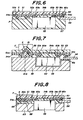
- Fig. 6 is a cross sectional view showing an example of the thermal head having a second structure. Also in this example, the printing surface S is formed to be flat.
- the printing section P, driving IC 55 and wiring section 53 are reinforced by adhering them with a resin 57 as an integral unit body.
- protection layers 54a, 54b, 54c, and 54d are formed such that the heat generating layer 51 in the printing section P, electrically conductive layers 52a and 52b and wiring section 53 are covered with the protection layers.
- the resin 57 of this second structure may be preferably made of epoxy resin, acrylic resin or silicone resin.
- the protection layers 54a, 54b, 54c, and 54d may be preferably made of SiOx, SiNx or a mixture thereof SiOxNy.
- Fig. 7 is a cross sectional view illustrating an embodiment of the thermal head having the principal structure according to the invention.
- the printing surface is formed to be smoothly protruded outwardly.
- a heat storage layer 58 is formed under a protection layer 54a, but the third structure contains thermal heads in which the protection layer or heat storage layer are dispensed with.
- the printing section P, driving IC 55 and wiring section 53 are reinforced by forming them as an integral unit body by means of a heat dissipating member 59. That is to say, the electrically conductive layer 52b and wiring section 53 are electrically connected to the driving IC by means of connecting portions 60a and 60b, the wiring section 53 is electrically connected to the wire 56 by means of a connecting portion 60c, and the printing section P, driving IC 55 and wiring section 53 are secured to the heat dissipating member 59 with the aid of adhesive layer 61a and fixing member 61b. Further, the driving IC 55 and the protection layer 54b are secured to each other by filling a resin, preferable a silicone resin 62 therebetween.
- the fixing member 61b is composed of a both-sided adhesive tape, but it may be also formed by an adhesive agent such as silicone adhesive or viscoelastic rubber.
- the adhesive layer 61a is preferably made of epoxy resin, acrylic resin, and silicone resin considering a thermal conductivity of the heat storage layer 58 and heat dissipating member 59, but may be made of an adhesive such as thermosetting resin, silicone adhesive, heat-resistant inorganic adhesive and viscoelastic rubber.
- the heat dissipating member 59 is preferably made of a material having a thermal conductivity not less than 6.27 ⁇ 10 4 J/m ⁇ h ⁇ °C such as Al, Cu, Ni, Fe, Mo and alumina ceramics. In the case that the heat dissipating member 59 is made of a metal, the fixing member 61b has to be electrically insulating, because the fixing member 61 is formed between the wiring 56 and the heat dissipating member 59.
- Fig. 8 is a cross sectional view illustrating an example of the thermal head.
- a printing surface S is formed to be flat.
- the printing section P is secured to a flat plate 65 by means of a resin 66 as an integral unit body.
- the driving IC 55 and electrically conductive layer 53 forming the wiring section are secured to the flat plate 65 with the aid of the resin 66.
- the flat plate 65 herein, means a member like a plate whose opposing surfaces are in parallel or substantially parallel with each other.
- the flat plate 65 Since the flat plate 65 has the function to reinforce the printing section P, driving IC 55 and wiring section as well as to dissipate the heat, the flat plate is preferably made of a material having a thermal conductivity not less than 6.27 ⁇ 10 4 J/m ⁇ h ⁇ °C such as Al, Cu, Ni, Fe, Mo or alumina ceramics like as the heat dissipating member 59 of the principal structure.
- the resins 62 and 66 are preferably made of epoxy resin, acrylic resin, and silicone resin.
- the protection layers 54a, 54b, 54c, and 54d are preferably made of SiOx, SiNx, or SiOxNx.
- the above mentioned heat storage layer 58 is preferably made of glass, resin such as polyimide and Bakelite (trade name).
- the heat storage layer is preferably made of a material having a thermal conductivity not higher than 4.18 ⁇ 10 4 J/m ⁇ h ⁇ °C.
- the heat storage layer is preferably made of a resin, for instance a polyimide containing alumina or metal powders for adjusting a thermal conductivity to a value within the above range.
- the printing section P having the wear-resistant layer 50, heat generating layer 51, electrically conductive layer 52a and 52b forming the electrodes and the wiring section 53 for performing the connection to the driving IC 55 and external circuit are arranged on a side of the wear-resistance layer 50 opposite to the printing surface S which is brought into contact with the thermal record medium. Therefore, on a side of the printing surface S, any part is not protruded from the wear-resistant layer 50, and thus the thermal head is not brought into contact with the thermal record medium and rubber roller for urge the record medium against the printing surface. Therefore, a whole size of the thermal head viewed in a traveling direction of the record medium can be small and the thermal head can be miniaturized.
- Fig. 9 is a schematic view showing a fact that the number of thermal heads according to the invention simultaneously manufactured in a single composite substrate can be greater than that of known thermal heads.
- Fig. 9A illustrates a case of manufacturing the conventional thermal heads and
- Fig. 9B shows a case of manufacturing the thermal heads according to the present invention.
- Fig. 10 is a schematic view showing a difference in size between the conventional thermal head and the thermal head according to the invention.
- Fig. 10A represents the known thermal head and Fig. 10B shows the thermal head according to the invention.
- Figs. 10A and 10B depict ones of the thermal heads shown in Figs. 9A and 9B, respectively on an enlarged scale. In Fig. 10, only the printing section P, printing surface S and driving circuit section D.
- a reference character a designates a lateral length of the composite substrate B, a reference character b a longitudinal length of the composite substrate B, reference characters L and L' a distance between the printing section S and the driving circuit section D of the known thermal head and the thermal head according to the invention, respectively and reference characters W and W' denote a width of the known thermal head and the thermal head according to the invention viewed in a travelling direction of the thermal record medium.
- the thermal heads are not manufactured separately, but after forming plural thermal heads on a composite substrate B having a certain size as shown in Fig. 9, the substrate is cut to obtain separate thermal heads.
- the composite substrate B means a substrate having a relatively large surface area such that plural thermal heads can be formed simultaneously.
- the distance L between the printing section P and the driving circuit section D is so long that the lateral length W of each thermal head is large as shown in Fig. 9A and 10A. Therefore, the number of the thermal heads obtained from a single composite substrate B is decreased and a manufacturing cost becomes expensive.
- the distance L' between the printing section P and the driving circuit section D is so short that the lateral length W' of each thermal head is short accordingly.
- the number of thermal heads manufactured from a single composite substrate B is increased and a manufacturing cost becomes decreased.
- Fig. 11 shows an example of the thermal head.
- a heat storage layer 58 is formed which is thermally coupled with a heat generating layer 51 constituting the printing section P.
- the remaining structure is similar to that of Fig. 5. That is to say, the heat storage layer 58 is formed under the heat generating layer 51 through the protection layer 54a. Therefore, the heat generated from the heat generating layer 51 is prevented from being transferred to the resin 57 and is retained within for a certain time period. In this manner, the heat storage layer 58 has to be formed near the heat generating layer 51. although it is sufficient to provide the heat storage layer 58 near the heat generating layer 52, it may be arranged beyond the heat generating layer.
- the heat storage layer 58 has a function for preventing the heat generated from the heat generating layer 51 from being transferred to the resin 57 and retaining the heat therein for a certain time period. Therefore, a thermal conductivity of the heat storage layer has to be low to a certain extent, in practice, has to be not higher than 4.18 ⁇ 10 4 J/m ⁇ h ⁇ °C.
- This heat storage layer 58 is preferably contain at least one of polyimide and glass, and more particularly, the heat storage layer may be made of a polyimide containing powders for adjusting a thermal conductivity.
- Fig. 12 is a cross sectional view showing an example of the thermal head.
- the printing surface S of the printing section P is formed flat and the heat dissipating body 68 is formed under the heat storage layer 58.
- the thermal head of this embodiment is identical with that shown in Fig. 6 except for the heat storage layer 58 and heat dissipating body 68.
- the heat dissipating body 68 is preferably made of a metal such as Al, Cu, Ni, Fe, and Mo or alumina ceramics.
- the heat stored in the heat storage layer is dissipated to the external, and thus a cooling rate of the printing section P during the heat dissipation can be made high.
- the "during the heat dissipation” means a condition in which an electric current does not flow through the heat generating layer 11.
- the heat dissipating body 68 is arranged to be directly contacted with the lower part of the heat storage layer 58, but may be provided via another layer such as adhesive layer having a high thermal conductivity.
- the adhesive layer is preferably made of a silicone or epoxy resin containing alumina or metal powders for adjusting a thermal conductivity.
- a part of the heat dissipating body 68 is preferably exposed from the resin 57.
- the heat dissipating body 68 serves to dissipate the heat stored in the heat storage layer 58 and to increase a cooling rate of the printing section P during the heat dissipation.
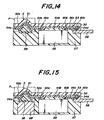
- Figs. 13, 14 and 15 are cross sectional views showing another embodiments of the thermal head according to the invention.
- the printing surface S has a smooth outwardly protruding surface.
- the thermal head according to the present invention although the thermal head has the printing surface S protruded outwardly, there is not formed a groove in the printing surface in the known thermal head shown in Fig. 2, but the smooth printing surface can be obtained. Thus, there can be attained a better contact between the printing surface S and the thermal record medium.
- the printing surface S is protruded outwardly.
- the thermal head can be brought into intimate contact with the thermal record paper, and therefore a heat can be efficiently transferred to the thermal record paper and a printing quality is improved.
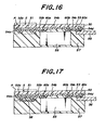
- Figs. 16, 17 and 18 show the thermal heads having the printing surface S formed to be flat.
- the example depicted in Fig. 16 corresponds to that shown in Fig. 6, the example illustrated in Fig. 17 corresponds to that shown in Fig. 11 having the heat storage layer 58, and the example depicted in Fig. 18 corresponds to that illustrated in Fig. 12 having the heat storage layer 58 and heat dissipating body 68.
- Figs. 19, 20 and 21 show the thermal heads having the printing surface S formed to be protruded outwardly.
- the embodiment shown in Fig. 19 corresponds to that illustrated in Fig. 13, the embodiment of Fig. 20 corresponds to that shown in Fig. 14 having the heat storage layer 58, and the embodiment illustrated in Fig.
- the heat generating layer 51 is arranged on the electrically conductive layers 52a and 52b viewed from the wear-resistant layer 50. It should be noted that an order to stacking these two layers is determined by the method of forming the heat generating layer 51 and a material constituting the electrically conductive layers 52a and 52b.
- the thermal head is reinforced by means of the heat dissipating member 59 and the flat plate 65, respectively.
- Functions and materials of the heat dissipating member 59 and flat plate 65 will be explained hereinbelow, mainly with reference to the flat plate 65.
- the flat plate 65 is formed under the heat storage layer 58 by interposing the resin 66 therebetween.
- the flat plate has the function of supporting the whole components of the thermal head mechanically and shortening a cooling time of the printing section P during the heat dissipation. By using the flat plate 65, therefore, a mechanical strength of the thermal head is improved and a printing speed is increased.
- the flat plate 65 with the above mentioned functions should have a proper mechanical strength and a relatively high thermal conductivity.
- a thermal conductivity of the flat plate 65 is preferably not less than 6.27 ⁇ 10 4 J/m ⁇ h ⁇ °C.
- the heat dissipating member 59 and flat plate 65 are not particularly limited, but may be formed in various shapes. Considering miniaturization, efficient heat transfer and reliability, however, they are preferably formed in such a shape that they are not brought into contact with the driving IC. For instance, a portion of these members corresponding to a position of the driving IC 55 may be depressed or cut out.
- the surfaces of the heat dissipating member 59 and flat plate 65 opposite to the resin 66 may be formed to have heat dissipating fins.
- a size of the heat dissipating member 59 and flat plate 65 may be properly determined considering the miniaturization, mechanical strength and heat dissipation.
- the heat dissipating member 59 and flat plate 65 are preferably made of a substance having a thermal conductivity not less than 6.27 ⁇ 10 4 J/m ⁇ h ⁇ °C as mentioned above. Such substances are listed in the following Table 1. It should be noted that a substance having a higher thermal conductivity can yield improved heat dissipation and heat-resistant characteristics, and therefore Al and Cu may be preferably used. Substance Al 2 O 3 Pb Fe Ni Al Cu Thermal conductivity ( ⁇ 10 4 J/m ⁇ h ⁇ °C) 7.6 12.5 24.2 32.1 73.2 13.9
- the printing surface S is formed into a concave shape and the heat storage layer 58 is provided below the printing section P.
- the printing surface S is formed to be flat and the heat storage layer 58 is formed below the printing section P.
- the printing surface S is formed to be convex and the heat storage layer 58 is formed below the printing section P like as the embodiment of Fig. 22, but an order of stacking the heat generating layer 51 and electrically conductive layers 52a, 52b is reversed to that of the embodiment illustrated in Fig. 22.
- the high temperature process herein, means a process of forming a film at a temperature not lower than 500°C.
- LPCVD Low Pressure Chemical Vapor Deposition
- a chemical vapor deposition is carried out at a low pressure.
- a stacking order of the heat generating layer and electrically conductive layer is determined by a melting point and the like of a substance constituting the electrically conductive layers 52a and 52b. This will be further described as follows.
- the heat generating layer 51 could not be formed after forming the electrically conductive layers.
- Aluminum may be given as a typical substance belonging to such a substance.
- the electrically conductive layers 52a and 52b are made of a metal having a low melting point, the electrically conductive layers has to be formed after forming the heat generating layer 51.
- the heat generating layer 51 could be formed after forming the electrically conductive layers 52a and 52b.
- Substances having a melting point not lower than 2800°C are preferably used, and W and Ta may be used.
- a melting point of W is 2990°C and that of Ta is 3400°C.
- the low temperature process herein, means a process of forming a film at a temperature not higher than 300°C.
- a typical example of such a film forming process at a low temperature is plasma CVD and sputtering.
- the plasma CVD herein, means Plasma-enhanced Chemical Vapor Deposition, and is one of the film forming method using the chemical vapor deposition.
- the heat generating layer 51 could be formed after or before forming the electrically conductive layers 52a and 52b.
- the flat plate may be formed to have the through hole at a position corresponding to the driving IC 55 as shown in Fig. 8.
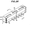
- Figs. 25 and 26 are perspective views showing the thermal head with the printing surface S is directed downward.
- a cross sectional view taken along A-A line in Fig. 25 corresponds to Fig. 8 or 23 wherein the printing surface S is formed to be flat and a cross sectional view taken along A-A line in Fig. 26 corresponds to Fig. 22 or 24 wherein the printing surface S is formed to be protruded outwardly.
- the thermal head according to the invention can be constructed to have any of the above explained first to fourth principal structures, and is not limited to the above embodiments shown in the drawings.
- various portions of the thermal head may be made of substances which have been used in the known thermal head.
- a FPC used in the known thermal head may be used as the wiring 56 for connecting the driving IC to an external circuit.
- the wiring 56 to an external circuit is preferably formed by terminals such as lead frame or metal stick.
- the lead frame may be made of generally used substances such as Fe alloy or Cu alloy. Among these substances, 42wt%Ni-58wt%Fe is preferable as the Fe alloy, and a substance adding Fe, Sn, and Zr to Cu is preferable as the Cu alloy.
- the metal stick may be made of generally used substances such as Fe, Cu and Al. It should be noted that metal stick may be made of the above mentioned alloys.
- the thermal head according to the invention In the method of manufacturing the thermal head according to the invention, a stacking order is reversed as compared with the conventional methods, and thus at first, the wear-resistant layer is formed.
- a substrate used as a support in the known thermal head is used as a tool for manufacturing the thermal head according to the invention.
- the method of manufacturing the thermal head according to the present invention includes the following five fundamental steps:
- a substrate is etched to have a desired shape corresponding to a shape of a printing surface.
- Si, glass, alumina and the like can be used as a material of the substrate. It is preferable to use a borosilicate glass because the borosilicate glass is cheap and can be easily removed by etching.
- step A-2 Formation of Sacrificial Layer for Peeling-off
- a sacrificial layer is formed on the substrate for separating the thermal head form the substrate after forming the thermal head.
- the sacrificial layer may be mande of MgO, CaO, ZnO and the like. Conventional methods like as sputtering may be used for forming the sacrificial layer.
- step B Formation of Main Components
- step B-1) Formation of Wear-resistant Layer
- a wear-resistant layer is formed by depositing SiC compound, SiB compound, SiO compound or SiON compound.
- Several conventional methods such as plasma CVD may be used for the formation of the wear-resistant layer.
- step B-2 Formation of Heat Generating Layer
- a heat generating layer is formed by depositing Ta, Ni-Cr or Nb-SiO2.
- Several known methods such as LPCVD, plasma CVD, and sputtering may be used for forming the heat generating layer.
- Dry-etching such as RIE (Reactive Ion Etching) is preferably used as the etching method for etching the heat generating layer into a desired pattern, but wet-etching may also be used.
- SF 6 , CF 4 , Cl 2 , O 2 or a mixture thereof may be generally used as an etchant of the dry-etching.
- the term "etchant”, herein, means a reactive gas used in the dry-etching.
- the heat generating layer may be made of a metal such as Ta or an alloy such as Ni-Cr or Nb-SiO 2 or may be made of Ti0 2 or BN.
- An electrically conductive layer may be made of W, Ta, Au, Al and the like. Several conventional methods such as sputtering may be used for forming the electrically conductive layer.
- the electrically conductive layer includes the electrically conductive layers 52a and 52b and the electrically conductive layer constituting wiring section 53.
- Wet-etching may be preferably used as the etching method for etching the electrically conductive layer, but dry-etching may also be used.
- H2SO 4 and HNO 3 may be used as an etchant of the wet-etching. Particularly a mixed acid solution of H 3 PO 4 , C 2 H 4 O 2 and HNO 3 may be used as an etchant for etching Al.
- etchant herein, means a solution used in wet-etching.
- the above metal may be, herein, used as a multi-layer.
- step B-4 forming protection layer
- the protection layer may be made of SiOx, SiNx, SiOxNy, and the like.
- a value of x is not, however, limited to the above mentioned range.
- a mixture of SiOx and SiNx termed as SiOxNy may be preferably used.
- the protection layer is formed by one or more of the above mentioned layers. Conventional methods such as LPCVD, plasma CVD and sputtering may be used for forming the electrically conductive layer.
- a wet-etching may be preferably used, but a dry-etching may be also used.
- HF and a mixed solution of HF and NH 4 F are generally used as an etchant of the wet-etching.
- the heat generating layer and electrically conductive layer can be isolated, and at the same time the diffusion of substances from the heat storage layer 58 or resin 57, 62, and 66 to the heat generating layer 51, electrically conductive layers 52a and 52b or wiring section 53 can be prevented, and therefore the characteristics of these layers can be maintained stable for a long time.
- the driving IC and other members can be prevented from being short-circuited, and thus a degradation of the electrically conductive layer due to a composition of the resin can be prevented although the electrically conductive layer is heated to a high temperature under such a condition that the electrically conductive layer is brought into contact with the resin and an electric current flows through the electrically conductive layer.
- step B-5 Connection of Wire to Driving IC and External Circuit
- step B-1 and step B-2 may be carried out in any suitable order in accordance with an order to stacking the heat generating layer 51 and electrically conductive layers 52a, 52b.
- the above mentioned two steps B-3 and B-4 may be performed in any order by suitably selecting a method of manufacturing the heat generating layer and a substance of the electrically conductive layer.
- the electrical connection between the wiring section 53 and the wiring 56 means a connection between the wiring section of the thermal head and tip portions of terminals connected to a cable, and does not include a connection between the wire 56 and an external circuit.
- the process of connecting the wire 56 to the cable may be carried out after separating the thermal head from the substrate.
- the heat storage layer may be made of a substance having a thermal conductivity not higher than 4.18 ⁇ 10 5 J/m ⁇ h ⁇ °C such as Bakelite (trade name), polyimide and glass or a mixture containing at least one of such substances.
- Bakelite trade name
- polyimide polyimide
- glass or a mixture containing at least one of such substances.
- Several conventional methods like screen printing may be used for forming the heat storage layer.
- step C-2 Provision of Heat Dissipation Body
- the heat dissipating body may be made of a substance having a thermal conductivity not higher than 4.18 ⁇ 10 5 J/m ⁇ h ⁇ °C such as Al, Mg, Cu and Mo and may be provided by using an adhesive agent. Since the printing section can be reinforced by providing the heat dissipating body, a next step D may be omitted. This step C may be performed in any suitable manner in order to form the thermal head into a desired shape.
- the printing section P, driving IC 55 and wiring section 53 may be reinforced with epoxy resin, acrylic resin, silicone resin, etc. and at least the printing section P may be fixed to the heat dissipating member 59 or flat plate 65 with adhesive or both-sided adhesive tape. It is preferable to use a resin having a coefficient of linear expansion after curing close to that of the substrate which is used as a tool for manufacturing the thermal head. This is due to a fact that by selecting the two substances having similar coefficients of linear expansion, a stress generated after hardening can be remained small.
- the printing section, driving IC and wiring section may be integrated into a single unit by means of the above resin producing a small stress, but when an amount of the resin is large, the substrate might be bent by the stress.
- Thermosetting adhesive, silicone adhesive, heat-resistant adhesive, viscoelastic rubber, etc. may be preferably used as the adhesive.
- the printing section P may be adhered to the heat dissipating member or flat plate with an adhere layer and at least a part of the driving IC section and wiring section may be secured to the supporting member by means of a resin.
- step E Separation of Thermal Head from Substrate
- step E-1) Peeling-off of Substrate by Removal of Sacrificial Layer
- the sacrificial layer is removed by etching the substrate such that the thermal head is independent from the substrate.
- Wet-etching which can perform a selective etching easily may be preferably used as the etching method.
- the wear-resistant layer acts as an etching stopper.
- the substrate may be etched effectively by removing a part of the substrate by a mechanical grinding, and then by removing all the remaining portion by a wet-etching. An etching efficiency may be increased by using an etching solution containing grinding balls, in such an etching a mechanical etching is also performed.
- the glass has a coefficient of heat expansion closer to those of the films formed in the printing section of the thermal head compared with a stainless steel, and thus an influences of heat expansion and heat shrinkage to the printing section is small and characteristics of the thermal head are influenced to a less extent. Moreover, a problem of damage during the separation does not occur as compared with the peeling-off, and the thermal head can be easily manufactured.
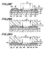
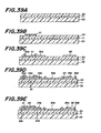
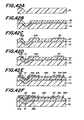
- Figs. 27A-27G show successive steps for manufacturing the thermal head having the flat printing surface S as shown in Fig. 6.
- step A-2 Formation of Sacrificial Layer for Peeling-off
- a provisional substrate 70 serving as a manufacturing tool was made of 7059 glass of Corning Company (barium borosilicate glass) as shown in Fig. 27A, and a MgO layer serving as the sacrificial layer 71 was formed on the substrate by sputtering. A thickness of this MgO layer was 2 ⁇ m.
- step B-1) Formation of Wear-resistant Layer
- a wear-resistant layer 50 was formed by depositing SiB layer and SiON layer by plasma CVD.
- the SiB layer and SiON layer were formed successively in this order.
- the SiB layer and the SiON layer were formed to have a thickness of 7 ⁇ m and 3 ⁇ m, respectively.
- step B-2 Formation of Heat Generating Layer
- a NbSiO 2 layer constituting the heat generating layer 51 was formed by sputtering. A thickness of the NbSiO 2 layer was 0.2 ⁇ m. The thus formed NbSiO 2 layer was etched into a desired pattern by RIE to form the heat generating layer 51 as shown in Fig. 27B. SF 6 was used as an etchant.
- an Al layer constituting the electrically conductive layers 52a and 52b and wiring section 53 was formed to have a thickness of 0.7 ⁇ m by sputtering, and then the Al layer was etched by wet-etching into a desired pattern to form the electrically conductive layers 52a and 52b as shown in Fig. 27C.
- a mixed acidic solution was used as an etchant.
- a SiO 2 layer constituting the protection layer 54a-54d was formed by plasma CVD.
- a thickness of the SiO 2 layer was 1.0 ⁇ m.
- the thus formed SiO 2 layer was processed by RIE to form the protection layers 54a-54d as shown in Fig. 27D.
- CHF 3 was used as an etchant.
- step B-5 Connection of Wires to driving IC and External Circuit
- the wires 56 for establishing the connection to the driving IC 55 and external circuit were connected as shown in Fig. 27E.
- the driving IC 55 was herein connected to the electrically conductive layer 52b and wiring section 53 through the connecting portions 60a and 60b by flip chip-bonding using solder-bump.
- the driving IC 55 had a size of 1mm ⁇ 5mm ⁇ 0.5mm.
- the wires 56 to the external circuit were connected to the wiring section 53 through the connecting portions 60c by soldering.
- step E-1) Peeling-off of Substrate by Removal of Sacrificial Layer
- the MgO layer serving as the sacrificial layer 71 for peeling-off was removed.
- wet-etching using a H 3 PO 4 solution was adopted.
- Figs. 28A-28H show successive steps of manufacturing the thermal head having the flat printing surface and the heat storage layer 58 provided under the printing section P as shown in Fig. 11.
- the (step A-2), (step B-1), (step B-2), (step B-3) and (step B-4) illustrated in Figs. 28A-28D were conducted in a similar manner to the embodiment shown in Fig. 27.
- a mixed polyimide layer constituting the heat storage layer 58 was applied by screen printing.
- the mixed polyimide layer was formed on the groove formed in the upper surface of the heat generating layer 51 via the protection layer 54a.
- a thickness of the mixed polyimide layer was 20 ⁇ m.
- the mixed polyimide layer was heated and hardened at a temperature of 400°C to form the heat storage layer 58.
- the mixed polyimide of this embodiment was the polyimide containing spherical alumina fillers to control a thermal conductivity of the protection layer.
- step B-5 shown in Fig. 28F, (step D) in Fig. 28G and (step E-1) illustrated in Fig. 28H were carried out in a similar manner to the steps depicted in Figs. 27E, 27F and 27G, respectively.
- step E-1 the thermal head shown in Fig. 11 was obtained.
- Figs. 29A-29I show successive steps of manufacturing the thermal head having the flat printing surface, heat storage layer 58 and heat dissipating body 68 as shown in Fig. 12.
- step A-2) and (step B-1) shown in Fig. 29A, (step B-2) illustrated in Fig. 29B, (step B-3) depicted in Fig. 29C, (step B-4) shown in Fig. 29D and (step C-1) illustrated in Fig. 29E were conducted in a similar manner to those shown in Figs. 28A-28E.
- the heat dissipating body 58 made of aluminum was adhered to the heat storage layer.
- a width of the heat dissipating body 68 made of Al was 1.0mm and an epoxy resin adhesive agent was used.
- step B-5 shown in Fig. 29G, step D) illustrated in Fig. 29H and (step E-1) depicted in Fig. 29I were performed in a similar manner to those shown in Figs. 28F-28H.
- step E-1 depicted in Fig. 29I were performed in a similar manner to those shown in Figs. 28F-28H.
- a surface of the heat dissipating body 68 remote from the adhesive layer was exposed from the resin 57.
- Figs. 30A-30H show successive steps of manufacturing the thermal head having the printing surface S protruded outwardly as shown in Fig. 13.
- the substrate serving as the manufacturing tool was made of a 7059 glass manufactured by Corning Company.
- a photoresist pattern was formed by photolithography and a groove having a substantially semicircular lateral cross section was formed by wet-etching.
- a negative resist was used in the photolithography and HF was used as an etchant. After etching the substrate 70, the photoresist was peeled-off.
- Figs. 31A-31H show successive steps of manufacturing the thermal head which comprises the outwardly protruded printing surface S as shown in Fig. 14 and includes the heat storage layer 58 provided under the printing section P.
- step A-1 shown in Fig. 31A was performed in a similar manner to that shown in Fig. 30A.
- step A-2) illustrated in Fig. 31B, (step B-1) in Fig. 31C, (step B-2) in Fig. 31D, (step B-3) in Fig. 31E, (step B-4) and (step C-1) in Fig. 31F, (step B-5) in Fig. 31G, (step D) in Fig. 31H and (step E-1) depicted in Fig. 31I were carried out in a similar manner to those shown in Figs. 28A-28H.
- the thermal head shown in Fig. 14 was obtained.
- Figs. 32A-32J show successive steps of manufacturing the thermal head which has the outwardly protruded printing surface S as shown in Fig. 15 and comprises the heat storage layer 58 and heat dissipating body 68 provided under the printing section P.
- step A-1) shown in Fig. 32A, (step A-2) in Fig. 32B, (step B-1) in Fig. 32C, (step B-2) in Fig. 32D, (step B-3) in Fig. 32E and (step B-4) illustrated in Fig. 32F were performed in a similar manner to those depicted in Figs. 31A-31F.
- the heat dissipating body 68 was adhered to the heat storage layer 58 as shown in Fig. 32G. This step was performed in a similar manner to that shown in Fig. 29F.
- Succeeding steps, that is, (step B-5) shown in Fig. 32H, (step D) in Fig. 32I and (step E-1) depicted in Fig. 32J were conducted in a similar manner to those shown in Figs. 29G-29I.
- the thermal head shown in ig. 15 was obtained.
- Figs. 33A-33I represent successive steps of manufacturing the thermal head having the flat printing surface S and including the heat storage layer 58 and heat dissipating body 68 provided under the printing section P and the electrically conductive layers 52a and 52b stacked on the heat generating layer 51 of the printing section P as shown in Fig. 18.
- the steps shown in Figs. 29A-29I were carried out except that (step B-3) shown in Fig. 33B and (step B-2) illustrated in Fig. 33C were conducted in a reverse order. That is to say, the (step A-2) and (step B-1) were first performed as shown in Fig. 33A were conducted in a similar manner to that illustrated in Fig. 29A, and then (step B-3) shown in Fig. 33B was carried out in the following manner.
- the W layer constituting the electrically conductive layers 52a and 52b was formed by sputtering.
- a thickness of the W layer was 0.3 ⁇ m.
- the thus formed W layer was wet-etched in accordance with a desired pattern to form the electrically conductive layers 52a and 52b and wiring section 53.
- HNO 3 was used as an etchant.
- the step B-2 was performed in a similar manner to that shown in Fig. 29B. Succeeding steps, that is, (step B-4) shown in Fig. 33D, (step C-1) in Fig. 33E, (step C-2) in Fig.
- step B-5 in Fig. 33G (step D) in Fig. 33H and (step E-1) illustrated in Fig. 33I were carried out in a similar manner to those depicted in Figs. 29D-29I.
- step E-1) illustrated in Fig. 33I were carried out in a similar manner to those depicted in Figs. 29D-29I.
- Figs. 34A-34J show successive steps of manufacturing the thermal head having the protruded printing surface S and including the heat storage layer 58 and heat dissipating body 68 provided under the printing section P and the electrically conductive layers 52a and 52b stacked on the heat generating layer 51 of the printing section P as illustrated in Fig. 21.
- steps shown in Figs. 34B-34J were carried out in a similar manner to those illustrated in Figs. 33A-33I.
- the thermal head shown in Fig. 21 was obtained.
- the thermal head having the second principal structure according to the invention are shown. It should be noted that the thermal head with the second principal structure, but without the heat dissipating body 68 as shown in Figs. 17 and 20 and the thermal head with the second principal structure, but without the heat storage layer 58 and heat dissipating body 68 as shown in Figs. 16 and 19 may be manufactured by conducting steps similar to those of the above embodiments.
- the sacrificial layer 71 for peeling-off was used in separating the thermal head from the substrate 70, but according to this invention, the etching may be also used in removing the substrate 70.
- the wear-resistant layer acts as an etching stopper, the etching can be carried out easily.
- the substrate 70 may be removed by performing the etching with HF.
- the thermal head was separated from the substrate 70 by such a process.
- Figs. 35A-35F show successive steps of another embodiment of the method of manufacturing the thermal head according to the invention.
- the substrate 70 made of a borosilicate glass was prepared, on which the wear-resistant layer 50 consisting of SiB layer and SiON layer was formed as shown in Fig. 35B, and then the heat storage layer 51 made of NbSiO 2 was formed.
- the electrically conductive layers 52a and 52b made of aluminum were formed on the heat generating layer 51, and a supporting layer 75 made of polyimide resin, acrylic resin or glass having a low melting point was formed as shown in Fig. 35E.
- the substrate 70 was removed over a depth of h1 by mechanical grinding using a whetstone, and the remaining portion of the substrate was removed over a depth of h2 by wet-etching.
- the substrate 70 can be efficiently removed.
- the printing section may be attached to another structural member 77 with an adhesive layer 76. Then, a degree of freedom in arrangement can be improved.
- Figs. 36A-36H are cross sectional views showing successive steps of another embodiment of the method of manufacturing the thermal head according to the present invention.
- steps shown in Figs. 36A-36D are similar to those illustrated in Figs. 35A-35D in the previous embodiment 9.
- the protection layers 54a and 54b were formed and another electrically conductive layer 78 was formed such that it is contacted with the extended part of the electrically conductive layer 52b, and after the heat storage layer 58 was formed on the protection layer 54a of the printing section as shown in Fig. 36F, a polyimide resin constituting the supporting layer 75 was formed as illustrated in Fig.
- the electrically conductive layer 78 for connecting the electrically conductive layer 52b of the printing section to an external circuit may be separately formed from the electrically conductive layers 52a and 52b.
- the electrically conductive layer 78 may be connected to the driving IC on a side of the wear-resistant layer 50 which is opposite to the printing surface S or same as the printing surface S.
- Figs. 37A-37G show another embodiment of the method of manufacturing the thermal head according to the invention.
- the groove 70a was formed in the surface of the substrate 70 as shown in Fig. 37A, and then the wear-resistant layer 10 was formed on the substrate 70 including the groove surface as illustrated in Fig. 37A.
- the heat generating layer 51 was formed as shown in Fig. 37C, and after forming the electrically conductive layers 52a and 52b as shown in Fig. 37D, the heat storage layer 58 was formed to cover the heat generating layer 51 and electrically conductive layers 52a and 52b along the groove 70a and the leveling (uniformity in a thickness) was done by utilizing the liquidity of the heat storage layer as shown in Fig. 37E.
- the heat dissipating body 68 made of aluminum was adhered with the adhesive 79 as shown in Fig. 37F.
- a distance therebetween can be shortened and an efficiency of heat dissipation was improved.
- the substrate 70 was removed only by the wet-etching or by a combination of mechanical grinding and wet-etching. In this embodiment, a uniform thickness of the heat storage layer 58 can be attained.
- the printing section P, driving IC 55 and wiring section 53 are reinforced by means of the heat dissipating member 59.
- Figs. 38A and 38B are cross sectional views showing steps near the final step of this embodiment.
- the driving IC 55 and the wires 56 were provided.
- metalized layers 80a, 80b and 80c were formed on the electrically conductive layer 52b and wires 56, and the flip chip-bonding was done with solder-bumps 81a, 81b and 81c.
- the step of forming the metalized layers 80a-80c is a step of forming metal layers on the electrically conductive layer 52b and wires 53, said metal layers reacting with the solder bumps 81a-81c to form good electrical connections.
- a reference numeral 84 denotes a common electrode which is connected to the electrically conductive layer 52a formed commonly to plural heat generating elements constituting the heat generating section.
- the common electrode 84 and wires 56 formed beside the printing section P were secured to the inner surface of the heat dissipating member 59 made of aluminum by means of both-sided adhesive tapes 82 and 83, and spaces formed between the printing section P, driving IC 55 and wiring section 53 were filled with a silicone resin 62 such that these components were reinforced.
- a groove 59a In an inner surface of the heat dissipating member 59, there were formed a groove 59a at a position opposing to the heat storage layer 58 of the printing section P as well as a recessed part 59b into which a part of the driving IC 55 was projected. In this manner, the driving IC 55 is covered with the heat dissipating member 59 and is not exposed.
- the common electrode 84 and wires 56 are simply secured to the heat dissipating member 59 by means of the both-sided adhesive tapes 82 and 83, and therefore they can be constructed by an automatic machine.
- an adhesive agent may be used as the fixing member instead of the both-sided adhesive tapes 82 and 83. Since the heat storage layer 58 of the printing section P is connected to the heat dissipating member 59 by means of the resin 62 having a good thermal conductivity, a heat dissipating property of the printing section P is improved.
- the electrically conductive layers and wiring section can be prevented from be degraded in accordance with a composition of resin when the electrically conductive layers and wiring section are heated to a high temperature by flowing a current through the resin 62 which is brought into contact with the electrically conductive layers and wiring section.
- the whole thermal head except for the substrate 70 was covered with an etching resist 85.
- the etching resist 85 may be made of resists manufactured and sold by Nikka Seiko Company under trade names of "Black Mask” and "Protect Wax”.
- the etching resist was removed by using xylene as a solvent as shown in Fig. 38B. In this manner, the thermal head portion is molded with the resin 62 not wholly but partially, and after covering the thermal head portion with the etching resist 85, the substrate 70 is removed.
- the reinforcement of the thermal head can be attained by supporting the printing section P, driving IC 55 and wiring section 53 by the flat plate 59.
- Figs. 39A-39H are cross sectional views showing successive steps of manufacturing the thermal head shown in Fig. 7.
- step A-2 Formation of Sacrificial Layer for Peeling-off
- the sacrificial layer 71 made of MgO was formed by sputtering on the substrate 70 made of the 7059 glass manufactured by Corning Company, which serves as the tool for manufacture.
- a thickness of the MgO layer was, herein, 2 ⁇ m.
- step B-1) Formation of Wear-resistant Layer
- a SiB layer and a SiON layer constituting the wear-resistant layer 50 were formed successively by plasma CVD.
- the SiB layer and the SiON layer were formed to have a thickness of 7 ⁇ m and 3 ⁇ m, respectively
- step B-2 Formation of Heat Generating Layer
- a NbSiO 2 layer constituting the heat generating layer 51 was formed on the wear-resistant layer 50 by sputtering.
- a thickness of this NbSiO 2 layer was 0.2 ⁇ m.
- the thus formed NbSiO 2 layer was dry-etched by RIE to form the heat generating layer 51 of the printing section. Upon etching, CHF 3 was used as an etchant.
- an aluminum layer constituting the electrically conductive layers 52a and 52b and wiring section 53 was formed by sputtering. A thickness of the aluminum layer was 0.3 ⁇ m. Then, the thus formed aluminum layer was wet-etched to form the electrically conductive layers 52a and 52b and wiring section 53 as shown in Fig. 39C. In this etching, a mixed acidic solution was used as an etchant.
- a SiO 2 layer constituting the protection layer was formed by plasma CVD. A thickness of the SiO 2 layer was 0.6 ⁇ m. Then, the SiO 2 layer was wet-etched to form the protection layers 54a, 54b, 54c, and 54d. In this etching, HF was used as an etchant.
- a mixed polyimide layer constituting the heat storage layer was applied by screen printing.
- the mixed polyimide layer was provided on the groove portion formed in the upper surface of the heat generating layer 51 through the electrically conductive layer 54a.
- a thickness of the mixed polyimide layer was 20 ⁇ m. Then, this layer was hardened by heating it at 350°C and the integrally united assembly was obtained as shown in Fig. 39E.
- the mixed polyimide used in this embodiment is a polyimide having spherical alumina fillers mixed therein.
- step B-5 Connection of Wires to Driving IC and External
- the wires 56 were connected to the driving IC 55 and the external as shown in Fig. 39F.
- the driving IC 55 was connected by flip chip-bonding to the electrically conductive layer 52b and wiring section 53 through the connecting portions 60a, 60b, and 60c.
- the driving IC 55 had a size of 1.0mm ⁇ 5.0mm ⁇ 0.5mm.
- the wires 56 made of Cu to the external circuit were connected to the wiring section 53 through the connecting portions 60c formed by soldering.
- the thus formed components were adhered to the flat plate 65 made of aluminum with the epoxy resin 66 and an assembly was heated to harden the epoxy resin to form an integrally united structure.
- the hardening was effected at 150°C.
- the flat plate 65 made of aluminum has an opening at a position corresponding to the driving IC 55, and had a size of 5mm ⁇ 90mm which is equal to a size of the thermal head and a thickness of 5 mm.
- step E-1 Separation of Substrate by Removing Sacrificial Layer
- the sacrificial layer 71 made of MgO was removed by etching with a H 3 PO 4 aqua-solution, and the thermal head was made independent from the substrate 70.
- Figs. 40A-40I are cross sectional views showing successive steps of manufacturing the thermal head shown in Fig. 22.
- the thermal head illustrated in Fig. 22 has the printing surface S which is protruded outwardly and the heat storage layer 58.
- the substrate 70 serving as the manufacturing tool was made of the 7059 glass manufactured by Corning Company.
- a resist pattern was formed by photolithography and a groove having a substantially semicircular lateral cross section was formed by wet-etching as shown in Fig. 40A.
- a negative-resist was used and HF was used as an etchant. After etching the substrate 70, the resist was peeled off.
- Figs. 41A-41H show successive steps of manufacturing the thermal head illustrated in Fig. 23.
- the thermal head shown in Fig. 23 has the flat printing surface S and the heat storage layer 58.
- the heat generating layer 58 is formed on the electrically conductive layers 52a and 52b viewed from the wear-resistant layer 50.
- Steps shown in Figs. 41A-41E are similar to those illustrated in Figs. 33A-33E in the embodiment 7 and steps of Figs. 41F-41H are similar to those depicted in Figs. 39F-39H in the embodiment 13.
- Figs. 42A-42H show successive steps of manufacturing the thermal head shown in Fig. 24.
- the thermal head of Fig. 24 has the outwardly protruded printing surface S and the heat storage layer 58.
- the heat generating layer 58 is formed on the electrically conductive layers 52a and 52b viewed from the wear-resistant layer 50.
- Steps shown in Figs. 42A-42F are similar to those illustrated in Figs. 34A-34F in the embodiment 8 and steps shown in Figs. 42G-42I are similar to those depicted in Figs. 40G-40I in the embodiment 13.
- the thermal conductivity of the flat plate 65 is denoted on the horizontal axis in logarithm scale and the dot broken ratio is denoted on the vertical axis.
- the dot broken ratio means a ratio of the number of broken heat generating elements to the number of the whole heat generating elements in percentage after flowing a current for 5000 hours.
- the heat generating layer 51 comprises an array of heat generating elements arranged with a pitch of 6 dots/mm and having a length of 85.3 mm.
- the dot broken ratio is decreased rapidly when the thermal conductivity of the flat plate 65 is higher than about 4.18 ⁇ 10 4 J/m ⁇ h ⁇ °C and the ratio is substantially 0% when the thermal conductivity is about 4.18 ⁇ 10 4 J/m ⁇ h ⁇ °C, and more particularly the ratio is perfectly 0% when the thermal conductivity is not less than 6.27 ⁇ 10 4 J/m ⁇ h ⁇ °C.
- the thermal conductivity of the flat plate 65 has to be higher than 4.18 ⁇ 10 4 J/m ⁇ h ⁇ °C and more particularly it is preferably not less than 6.27 ⁇ 10 4 J/m ⁇ h ⁇ °C.
- the relationship between the thermal conductivity of the flat plate 65 and the dot broken ratio may be equally applied to the relationship between a thermal conductivity of the heat dissipating member 59 and a dot broken ratio.
- Characteristics of the several embodiments of the thermal head according to the present invention have been evaluated and its results are shown in the following Table 2. The evaluation has been conducted by using a print test pattern having a print surface area of 50 %. Structure of thermal head Figure of embodiment Shape of printing surface Heat storage layer Heat dissipating member Power consumption [W/dot] Print speed [cm/sec] Print quality 1 Fig. 6 flat no no 0.18 2.5 good 2 Fig.8 flat yes yes 0.08 4.5 good 3 Fig. 11 flat yes no 0.08 2.0 good 4 Fig.
- thermal head according to the invention As shown in the Table 2, all the embodiments of the thermal head according to the invention have practically usable printing performance.
- the thermal head having any principal structures according to the present invention has superior characteristics to any conventional thermal heads.
- the printing quality can be improved by using the outwardly protruded printing surface S than the flat printing surface. It is considered that the outwardly protruded printing surface can be brought into intimate contact with a thermal paper and thus is better in the printing surface S like projecting, and thus a resolution of print is improved. In this manner, the printing section is preferably protruded outwardly.
- the embodiment having the heat storage layer 58 has a smaller electric power consumption than the embodiment without the heat storage layer. This is due to a fact that the heat storage layer 58 can prevent the diffusion of heat, and therefor an efficiency of electric power is improved. Furthermore, by providing the heat storage layer 58, a degradation in a quality of print due to a thermal deformation of the resin can be prevented. Therefore, it is preferable to provide the heat storage layer 58.
- the embodiments shown in Figs. 15 and 21 are particularly preferable, because in these embodiments, the printing surface is protruded outwardly and the heat storage layer 58 and heat dissipating body 68 are provided, Moreover, the embodiments shown in Figs. 22 and 24 are particularly preferable, because in these embodiments the printing surface is protruded outwardly and the heat storage layer 58 and flat plate 65 are provided. It is matter of course that according to the present invention, the most suitable embodiment may be selected from many embodiments in accordance with a required performance and manufacturing process.
- the thermal head can be easily manufactured by an automatic assembling machine, and therefore a manufacturing cost can be decreased.
- the number of the thermal heads obtained from a single composite substrate B can be increased. This will be further investigated in the following.
- the driving IC 55 and the wiring section 53 to external circuit are provided on a side of the thermal head opposite to the printing surface S. Therefore, upon printing, the driving IC and its electric connection are not brought into contact with a thermal paper and the like, and the driving IC can be closer to the printing section P.
- a size of the thermal head can be about 1/4 of the conventional thermal head, and therefore the number of the thermal heads obtained from a single composite substrate B can be increased twice as compared with the conventional thermal head.
- effect 4 A mechanical strength of the thermal head can be improved, and a heat dissipating property can be also improved.
- the heat dissipating layer can be formed in accordance with a configuration of the printing section P, driving IC and wiring section and manufacturing steps.
- effect 5 The thermal head having the smooth printing surface S which is brought into good contact with a thermal paper can be obtained without special steps and operation.
- the method of manufacturing the thermal head according to the invention can expect the following additional advantageous effect.
- effect 6) By using the step of peeling-off the substrate to make the thermal head independent from the substrate, since the substrate can be used repeatedly, a manufacturing cost can be decreased.
- effect 7) After removing mechanically a part of the substrate, a part or a whole of the remaining portion of the substrate is removed by wet-etching, and the substrate can be efficiently removed.
- the substrate made of a glass since the glass has a coefficient of thermal expansion closer to those of the layers constituting the printing section of the thermal head as compared with stainless steel, the printing section can be prevented from being influenced by thermal expansion and shrinkage, and therefore the characteristics of the thermal head are not influenced.
- effect 8 By using the substrate made of Si, glass or alumina, the printing section is not influenced by the thermal expansion and shrinkage during the manufacture and characteristics of the thermal head are not influenced, because the above materials have a coefficient of thermal expansion which is closer to those of materials constituting the printing section.
- effect 9 Since after forming the supporting layer on the heat generating layer and electrically conductive layer, the substrate is removed, the arrangement of the printing section P is not influenced by the driving IC, and thus the thermal head having a higher freedom of arrangement can be obtained.
Landscapes
- Engineering & Computer Science (AREA)
- Microelectronics & Electronic Packaging (AREA)
- Manufacturing & Machinery (AREA)
- Electronic Switches (AREA)
Abstract
Description
- This invention relates to a thermal head for use in a thermo-recording machine such as printer and facsimile and a method of manufacturing the same, and more particularly to a thermal head comprising a printing section including a wear-resistant layer having a printing surface to be brought into contact with a thermal record medium, a heat generating layer for generating heat to be transmitted to the thermal record medium through the wear-resistant layer and an electrically conductive layer connected to the heat generating layer, a driving circuit section connected to the electrically conductive layer of the printing section to control a heating electric power to be supplied to the printing section, and a wiring section for connecting the driving circuit section to an external circuit and a method of manufacturing such a thermal head.
- A thermal head is an equipment, in which heat generated in accordance with a supplied electric signal is transmitted to a thermal record medium, for instance a thermal paper to record characters and figures of desired shapes. A conventional thermal head is composed of the following basic components:
- A printing section includes a printing surface to be brought into contact with a thermal paper and generates and transmits heat for coloring the thermal paper.
- A driving circuit section supplies an electric power according to an electric signal bearing information to be printed. Here, the information is to be understood to mean image data representing characters and figures. Since normal semiconductor integrated circuit chips are used as the driving circuit, the driving circuit is denoted as a driving IC for the sake of simplicity in the present specification.
- A wiring section is provided for connecting the thermal head to a connector of a cable to be connected to an external circuit. The printing information and electric power are supplied to the thermal head from the external circuit via the wiring section. A connection to the external circuit is performed by a lead wire such as a flexible FPC (Flexible Print Circuit), and in this case, the wiring section includes pin-like conductors to be connected to the connector of the lead wire, a part of said pin-like conductors being exposed from the thermal head.
- Several examples of conventional thermal heads will be explained hereinbelow.
- Fig. 1 is a cross sectional view showing a structure of an example of the conventional thermal head, in which a driving IC is connected to a printing section and a wiring section by means of wire-bonding. The thermal head shown in Fig. 1 has been used in a usual type thermo-recording printer. In Fig. 1. a
reference numeral 10 denotes a wear-resistant layer having anti-physical and anti-chemical characters, a reference numeral 11 a heat generating layer,reference numerals reference numeral 13 an electrically conductive layer constituting a wiring section for connecting the thermal head to an external circuit, areference numeral 14 solders constituting connecting portions for connecting the wiring section and a wiring cable with each other, a reference numeral 15 a driving IC, a reference numeral 16 a wiring for connecting the driving to the external circuit, a reference numeral 17 a heat storage layer, a reference numeral 18 a resin layer for isolating and protecting the driving IC and bonding wires, areference numeral 19 an electrically insulating substrate, areference numeral 20 bonding wires connecting terminals of the driving IC to the electricallyconductive layer 12b and wiring section, a reference numeral 21 a thermal paper, and areference numeral 22 represents a rubber roller for urging the thermal paper against the thermal head. A reference character P shows a printing section which is composed of a part of the wear-resistant layer 10, the heat generating layer 11 and parts of the electricallyconductive layers resistant layer 10 which is brought into contact with thethermal paper 21. A reference character L expresses a distance between the printing section P and theresin layer 18 protecting the drivingIC 15. - In the known thermal head shown in Fig. 1, the
heat storage layer 17 is formed on thesubstrate 19, on which the heat generating layer 11, electricallyconductive layers resistant layer 10 constituting the printing section P are successively stacked. The thermal head shown in Fig. 1 will be further explained by dividing it into several components. - (Component I) Printing Section
- (Component II) Driving IC
- (Component III) Wiring Section to External Circuit
- (Component IV) Heat storage Layer
- (Component V) Substrate And particularly the printing section is constructed by stacking the following layers:
- (I-1) Wear-resistant Layer
- (I-2) Heat Generating Layer
- (I-3) Electrically Conductive Layer
-
- Therefore, the conventional thermal head illustrated in Fig. 1 is composed not only of the basic components (Component I), (Component II), and (Component III), but also by the heat storage layer of (Component IV). These components are arranged on the
substrate 19 of (Component V). In other words, the (Component I)-(Component IV) are supported as a unit body by means of the (Component V). - The
heat storage layer 17, however, is an additional component for attaining a power save. There are also proposed thermal heads, in which a heat radiating or other components for increasing a printing speed. By providing such a component, a performance of the thermal head can be improved. The heat generating layer 11 constituting the printing section P is divided into many heat generating elements in a direction normal to a plane of the drawing of Fig. 1. The electricallyconductive layer 12a form a common electrodes to these heat generating elements and the electricallyconductive layer 12b constitutes divided electrodes each being connected to respective heat generating elements in order to flow an electric current only through one or more desired heat generating elements according to the print information. The common electrode and divided electrodes are called the electrically conductive layer in a general term in this specification. - Subsequently, functions of respective components will be explained.
- At first, respective layers constituting the printing section P of (Component I) will be discussed.
- The wear-
resistant layer 10 is brought into contact with thethermal paper 21 to transmit the heat generated by the heat generating layer 11 to the thermal paper. Therefore the printing surface S is composed of the surface of the wear-resistant layer 10 situating in the printing section P. The wear-resistant layer 10 is required to have a basic characteristic that the layer does not chemically react to components contained in the thermal paper. Moreover good wear-resistant and heat-resistant characteristics, a lower coefficient of friction and a proper hardness are required for the wear-resistant layer. Furthermore, the wear-resistant layer preferably has a suitable electrical conductivity. This is due to a reason that dusts and charged particles might adhered to the printing surface S by an electrostatic charge caused by a friction between the printing surface and the thermal paper, said dust and particles causing a degradation in a print quality and undesired wear. Therefore, in order to prevent the charging, the wear-resistant layer preferably has a proper electric conductivity. However since an extended portion of the wear-resistant layer extending from the printing section P is brought into contact with respective electrodes of the electricallyconductive layer 12b, the wear-resistant layer should have such a resistance that these electrodes are not short-circuited. - The heat generating layer 11 has a function of generating heat for coloring the thermal paper. The principle of the heat generation is based on the Joule heat, wherein heat is generated by flowing an electric current through a resistive body. Accordingly the heat generating layer 11 is required to have a stable electric property around 400°C. Here, the electric property mainly means a resistance and its change with time.
- The electrically
conductive layers conductive layer 12a constitutes the common electrode which commonly connects one ends of respective heat generating elements of the heat generating layer 11 to, for instance the ground potential point. The electricallyconductive layer 12b constitutes many electrodes for connecting respective heat generating elements of the heat generating layer 11 to the drivingIC 15 separately. To this end,bonding wires 20 are soldered to the electricallyconductive layer 12b and driving IC 15. - Since the electrically
conductive layers resistant layer 10. Consequently theconductive layers - The electrically
conductive layer 13 constituting the wiring section is soldered to the drivingIC 15 andbonding wires 20, and is also connected to wires, for instance thepins 16 bysolders 14 for establishing a connection to the external circuit. - The
heat storage layer 17 has a function for holding the heat generated by the heat generating layer 11 for a certain time period and preventing the heat from being transmitted to the drivingIC 15 through theresin layer 18. Thus theheat storage layer 17 should have a low thermal conductivity and a high heat-resistance. - The
substrate 19 constitutes fundamentally a supporting body of the thermal head. That is to say, the substrate has a function for supporting the printing section P, drivingIC 15, electricallyconductive layer 13 constituting the wiring section for connecting the thermal head to the external circuit,wires 16 connected to the wiring section. The substrate may be heated to about 400°C during the manufacturing process. Thus thesubstrate 19 should have a high mechanical strength as well as a high heat-resistance. Moreover, the substrate preferably has a high thermal conductivity such that the heat generated by the thermal head during the printing operation could be dissipated. - The
resin layer 18 is used to protect the drivingIC 15 and thebonding wire 20, and thus the resin layer should have a proper mechanical strength and a certain electrically insulating property. - Now substances composing respective components of the thermal head, that is to say, respective layers of the printing section P and
substrate 19 will be described. These components of the thermal head are made of substances which can satisfy the above mentioned characteristics. - Although the wear-
resistant layer 10 is preferably made of a substance which satisfies all the desired conditions mentioned above, such a substance could hardly be found. SiC based compound, SiB based compound, SiO based compound and SiON based compound may be listed as a substance which can satisfy the conditions to a relatively large extent. - The heat generating layer 11 has to be made of a substance which reveals a stable electric property at about 400°C. The heat generating layer is made of a metal such as Ta, an alloy such as Ni-Cr, a poly-Si and a mixture of a transition element and SiO2 such as Nb-SiO2. Among these substances, Nb-SiO2 has been generally used, because its resistance can be easily controlled.
- The electrically
conductive layer wiring section 13 should be made of a substance also having a stable electric property at about 400°C. W, Ta, Au, Al and the like may be listed as such a substance. - In order to attain a desired resistance value and an easy connection to the driving
IC 15, a multiple layer of the above stated metals may be used. - The
heat storage layer 17 has to be made of a substance having a small thermal conductivity as well as a high heat-resistant property. Bakelite, polyimide, glass and the like may be listed as such a substance. The Bakelite is a trade name of phenol-formaldehyde. Glass has been generally used due to its hardness. - The
substrate 19 should be made of a substance having a high thermal conductivity and a high heat-resistance. MgO, ZnO, aluminum nitride, alumina ceramics and the like may be listed for such a substance. The alumina ceramics have been generally used due to its easy processing and low cost. - Now a contact between the printing surface S of the printing section P and the
thermal paper 21 during the printing operation will be explained. - The printing in the thermal head is carried out by conducting the heat generated by the heat generating layer 11 to the
thermal paper 21 through the wear-resistant layer 10. Accordingly, in order to achieve a clear printing, the heat generated by the heat generating layer 11 has to be efficiently transmitted to thethermal paper 21. The more tight the contact between the printing surface S of the printing section P and thethermal paper 21 is, the better the heat transmission to thethermal paper 21 becomes. Therefore, the tight contact between the printing surface S of the printing section P and thethermal paper 21 has to be achieved by proper means. A method of making a tight contact between the printing surface S and thethermal paper 21 will be described while a facsimile is taken as an example. - In a machine in which the printing section P is arranged along a lateral line like as facsimile, the
thermal paper 21 is generally urged against the printing surface S of the printing section P by means of therubber roller 22. Therubber roller 22 also serves as a paper feeder. Accordingly upon designing therubber roller 22, the hardness and shape of therubber roller 22 are determined such that the tight contact can be attained between the printing surface S and thethermal paper 21 as far as possible. - Next, a method of establishing a connection to the driving
IC 15 will be described with reference to Figs. 2 and 3 in addition to Fig. 1. Figs. 1-3 are cross sectional views showing the structure of known thermal heads. In the thermal heads depicted in Figs. 2 and 3, the drivingIC 15 is connected by means of the wire-bonding, and particularly the thermal head illustrated in Fig. 2 has the printing section which is higher than that of the thermal head shown in Fig. 1. In the thermal head illustrated in Fig. 3, the driving IC is connected by means of the flip chip bonding. Portions of the thermal heads shown in Figs. 2 and 3 similar to those of Fig. 1 are denoted by the same reference numerals used in Fig. 1. It should be noted that in Fig. 2, a reference character I denotes a height from the surface of thesubstrate 19 to the printing section S, a reference character H a height from the surface of the substrate to a top of a bonding wire loop, and a reference character X represents a depressed portion of the printing section. - The driving
IC 15 has been connected to the electricallyconductive layer 12b and electrically conductive layers of thewiring section 13 by means of the following methods. - In the wire bonding method, a metal wire called a bonding wire is fused to the terminals of the driving IC as well as to an electrically conductive layer at a predetermined position. The wire bonding has been widely used as the connection method for the driving IC. The wire-bonding is described in, for instance Japanese Patent Application Publication No. 6-78004. Figs. 1 and 2 show the driving
IC 15 connected by abonding wire 20. - The flip chip bonding is a connecting method, in which solder balls are formed on a lower surface of the driving IC to be connected and the balls are fused to the conductive layer. The method is described in, for instance "Oki Electric Research and Development", No. 138, Vol. 55, No. 2. Fig. 3 illustrates the driving
IC 15 connected by the flip chip bonding. - There has been further provided the following connecting method in addition to the above mentioned two methods.
- TAB means Tape Automated Bonding. The tape is a connecting part formed by covering plural metal wires with an insulating resin and both ends of the metal wires are exposed on both ends. In the TAB method, the terminals of the driving IC are simultaneously connected to the electrically conductive layers at predetermined positions.
- As mentioned above, Fig. 1 shows the driving IC connected by the wire bonding. As can be understood from Fig. 1, when a distance between the driving
IC 15 and the printing section P is small, the following defects might occur. - (1) As shown in Fig. 1, in the case that the driving
IC 15 and thebonding wire 20 are covered with theprotective resin 18, the resin might be brought into contact with thethermal paper 21 orrubber roller 22. - (2) On the other hand, in the case that the driving
IC 15 and thebonding wire 20 are not covered with theprotective resin 18, the driving IC and bonding wires might be brought into contact with thethermal paper 21 orrubber roller 22. -
- In each cases, there might be produced a problem that the bonding wires might be broken and adjacent electrically conductive layers might be short-circuited.
- In order to solve such a problem, there may be considered the following two solutions.
- In this case, the distance L has to be at least about 10 mm, so that the thermal head could not be further miniaturized.
- In this case, the height I of the printing surface S measured from the surface of the
substrate 19 has to be not less than 200 µm. Now methods of making the height I of the printing surface S larger will be explained. - First as shown in Fig. 2, the
heat storage layer 17 is formed on thesubstrate 19 such that its thickness is partially increased, and the printing surface S is formed on the heat storage layer such that the printing surface is protruded outwardly. Since the height H of a top of a loop of thebonding wires 20 is about 200 µm, the above problem could not be solved as long as the height I of the printing section P is not less than 200 µm. However, an actual height I of the printing surface S is about 50 µm. - In practice, if the height I of the printing surface S is made not less than 200 µm, surfaces of the heat generating layer 11 and electrically
conductive layers - In the case of forming the
heat storage layer 17 to have a partially hick portion, the depressed portion X is formed at a center of the printing surface S as shown in Fig. 2. Accordingly a tight contact could not be attained between the printing surface S and thethermal paper 21, and thus a print density might be reduced. - A solution for solving the problem of the depressed portion X in the printing section P is described in Japanese Patent Application Laid-open Publication No. 62-170361. In the solution, however, an addition process is required for forming a protruded portion on the
heat storage layer 17 having a partially thickened portion, said protruded portion compensating the depressed portion X, and the process might become complicated and expensive. - The above mentioned (Solution 1) and (Solution 2) could not solve the problems of the undesired contact of the
bonding wire 20 andresin 18 to thethermal paper 21 andrubber roller 22. - As explained above, in the example of Fig. 3, since the driving
IC 15 is electrically connected by the flip chip bonding, after the driving IC is directly bonded to theconductive layer 12b andwiring section 13, the drivingIC 15 is sealed with theresin 18. Therefore, theresin 18 might be brought into contact with thethermal paper 21 andrubber roller 22. - In order to avoid the undesired contact of the
resin 18 with thethermal paper 21 andrubber roller 22, the distance L between the driving IC and the printing section P has to be at least about 8 mm. Then, the thermal head could not be further miniaturized like as the above mentioned wire bonding. - Moreover a method of manufacturing the thermal head as shown in Fig. 4 is described in Japanese Patent Application Laid-open Publication No. 5-64905. In this method, a stainless steel plate is used as a
provisional substrate 30 for manufacturing the thermal head as shown in Fig. 4 and after grinding the surface of the stainless steel plate as a mirror surface, a peeling-off layer 31 is formed by electroplating of copper, on which the wear-resistant layer 10, the heat generating layer 11, and theconductive layers heat storage layer 32 made of a heat-resist resin is formed as shown in Fig. 4E. Then, analumina substrate 34 is adhered on theheat storage layer 32 with an adhesive 33 as shown in Fig. 4F, and thereafter theprovisional substrate 30 is peeled off at the interface of the peeled-offlayer 31 to expose the wear-resistant layer 10 as a printing surface. Moreover a part of the wear-resistant layer 10 remote from the printing surface is removed to expose a part of theconductive layer 12b, to which the driving IC is connected to complete the thermal head. - This conventional method of manufacturing the thermal head has the following problems.
- (1) It is very difficult to grind the stainless steel plate constituting the
provisional substrate 30 as a flat mirror surface. - (2) When a number of thermal heads are simultaneously manufactured, it is
very difficult to peel off the
substrate 30 mechanically, because a surface area of the substrate is large. - (3) A thickness and plating conditions of the Cu plating layer constituting
the peeled-off
layer 31 could not be easily managed. - (4) Since peeling-off process could not be applied to a thermal head in which the printing section is protruded like as a partial graze, the thermal head having such a protruded printing section could never be manufactured.
- (5) Since a thermal conductivity of the
provisional substrate 30 made of stainless steel is different from that of the printing section formed on this substrate, the printing section is liable to be deformed during manufacturing. - (6) Characteristics of the printing section are liable to be changed due to a
stress which is produced upon peeling off the
substrate 30 made of stainless steel and is applied to the printing section. - (7) Since the driving IC is arranged on a side of the printing surface of the wear-resistant layer like as the conventional thermal heads shown in Figs. 1-3, the distance L between the printing section and the driving IC could not be shortened and the problems mentioned above with reference to Figs. 1-3 are remained unsolved.
-
- In the known thermal heads, the problems of undesired contact of the driving IC itself as well as of the electric connection parts of the driving IC to the thermal paper must be solved, the thermal head has to be large to a certain extent and the printing section has to be projected largely.
- However, this solution results in the following difficulties.
- (1) The thermal head could not be miniaturized, and therefore a high manufacturing efficiency and a low manufacturing cost could not be realized.
- (2) Since the printing section of the thermal head could not be formed easily, it is difficult to further improve a printing quality.
- (3) According to the known manufacturing method, in which after forming the printing section by depositing the films on the stainless steel substrate, the substrate is peeled-off, there are not only the problems in difficulty of manufacturing and in the deformation, but also the problem in variation of characteristics of the printing section.
-
- US 4841120 discloses a thermal head having a heat generating resistor and a driving circuit both formed on one side of a substrate, and a thermal recording face formed on the other side of the substrate. The thermal recording farce is formed by grinding the substrate.
- Therefore, the present invention has for its object to provide a thermal head, in which although a size of the thermal head is made small, a driving IC and its electric connection parts are not brought into contact with a thermal paper and a rubber roller, and thus the electric equipment could be protected against the cutting-off and short-circuit and as a result of which, the manufacturing could be performed efficiently at a low-cost.
- It is another object of the invention to provide a thermal head having a smooth printing surface which could attain a good contact with a thermal paper
- It is still another object of this invention to provide a method of manufacturing such a thermal head in an easy and less expensive manner without special processes and operations.
- According to a first aspect of the present invention there is provided a thermal head comprising: a printing section including a wear-resistant layer having a first surface constituting a printing face to be brought into contact with a thermal record medium and a second surface opposite to the first surface, a heat generating layer formed on a side of the second surface of the wear-resistant layer and generating heat to be transmitted to the thermal record medium through the wear-resistant layer, and an electrically conductive layer formed on the same side of the wear-resistant layer as the second surface and connected electrically to the heat generating layer; a driving circuit section connected to the electrically conductive layer of the printing section to control a heat generating electric power to be supplied to said printing section, said driving circuit section being arranged on the same side of the wear-resistant layer as the second surface; and a wiring section for connecting the driving circuit section to an external circuit, said wiring section being arranged on the same side of the wear-resistant layer as the second surface, characterized in that the printing surface of the printing section is formed as an outwardly protruding curved surface.
- In the thermal head according to the invention, since the driving circuit section and wiring section are arranged on a side of the wear-resistant layer opposite to the side which is to be brought into contact with a thermal record medium, the driving circuit section and connecting wires could not be brought into contact with the thermal record medium and rubber roller, and therefore a distance between the printing section and the driving circuit section can be shortened and the thermal head can be miniaturized.
- Upon practicing the thermal head according to the invention, the thermal head can be classified into the following four groups in accordance with its principal structure.
- According to the first principal structure of the thermal head according to the invention;
said wear-resistant layer in the printing section has an extended part which extends beyond the printing section,
said electrically conductive layer has an extended part which extends on a side of the second surface of the wear-resistant layer,
said wiring section is provided on a side of the second surface of the extended part of the wear-resistant layer, and
said driving circuit part is composed of integrated circuit chips, terminals of which are connected electrically to the extended part of the electrically conductive layer and to the wiring section. - In the second principal structure of the thermal head according to the invention, the thermal head comprises a supporting member provided on a side of the second surface of the wear-resistant layer of the printing section for supporting the printing section, driving circuit section, and wiring section.
- Said supporting member may comprise a resin member for bonding and fixing the printing section, driving circuit section and wiring section integrally, and said resin member may be preferably made of epoxy resin, acrylic resin, or silicone resin.
- In the third principal structure according to the invention, said supporting member comprises a heat dissipating member and an adhesive layer for fixing at least said printing section to said heat dissipating member.
- According to the fourth principal structure of the thermal head according to the invention, said supporting member comprises a flat plate and an adhesive layer for fixing at least said printing section to the flat plate.
- In each of the above mentioned first to fourth principal structures of the thermal head according to the invention, said printing surface may be flat or may be protruded outwardly.
- In the above explained third and fourth principal structures, said adhesive is preferably made of a resin selected from the group of epoxy resin, acrylic resin and silicone resin. Furthermore, said adhesive resin may contain powders such as alumina powders for increasing a thermal conductivity. Moreover, in the third and fourth principal structures, said means for fixing the driving circuit section and a part of the wiring section to said heat dissipating layer or flat plate may be preferably formed in the supporting member. This fixing member may be advantageously formed by double-sided adhesive tape.
- Moreover, in the third and fourth principal structures of the thermal head according to the invention, said adhesive layer is preferably made of thermosetting adhesive agent, heat-resistant inorganic adhesive agent or viscoelastic rubber.
- In the thermal head according to the invention, said printing section may be constructed by stacking the wear-resistant layer, heat generating layer and electrically conductive layer or by stacking the wear-resistant layer, electrically conductive layer and heat generating layer in this order viewed from the printing surface.
- Furthermore, said printing section may comprise a protection layer on a side of the heat generating layer opposite to the printing surface, said protection layer preventing a diffusion of impurities into the heat generating layer. Said protection layer may be preferably made of at least one of SiNx and SiNx or a mixture thereof.
In the thermal head according to the invention, said printing section may include a heat storage layer thermally coupled with the heat generating layer through the protection layer. Said heat storage layer may contain at least one of polyimide and glass. Particularly, the heat storage layer may be preferably made of a polyimide containing powders for adjusting its thermal conductivity. - The thermal head according to the invention may further comprise a heat dissipating body thermally coupled with the heat storage layer on a side opposite to the printing surface. Said heat dissipating body may be preferably made of at least one of Al, Cu, Ni, Fe, Mo and alumina ceramics.
- In case of providing a heat dissipating member and flat plate, they may be preferably formed in such a shape that they are not directed contacted with the driving circuit section. Further, these heat dissipating body and flat plate may be preferably made of a material having a thermal conductivity not less than 6.27 × 10⁴ J/m-h-°C like as the above mentioned heat dissipating body, and particularly they may be made of Al, Cu, Ni, Fe, Mo and alumina ceramics.
- According to a second aspect of the present invention there is provided a method of manufacturing a thermal head comprising a printing section which includes a wear-resistant layer having a printing surface to be brought into contact with a thermal record medium, a heat generating layer which generates heat to be transmitted to the thermal record medium through the wear-resistant layer, and an electrically conductive layer connected to the heat generating layer; a driving circuit section connected to the electrically conductive layer in the printing section to control a heat generating electric power to be supplied to the printing section; and a wiring section which connects the driving circuit section to an external circuit; the method comprising: a step of forming the printing section, the wear-resistant layer, the heat generating layer and the electrically conductive layer of the printing section on a substrate such that the printing surface of the wear-resistant layer is opposed to a surface of the substrate and at least a part of the electrically conductive layer is exposed on a side remote from the substrate, wherein the wear-resistant layer is formed by deposition; a step of forming the wiring section on a side of the wear-resistant layer in the printing section remote from the substrate and providing said driving circuit section on the wiring section as well as on an exposed surface of the electrically conductive layer; and a step of separating said printing section, driving circuit section and wiring section from the substrate as an independent unit body.
- In a preferable embodiment of the method of manufacturing the thermal head according to the invention, said wear-resistant layer is formed on the surface of the substrate to have an extended portion extending beyond the printing section, said electrically conductive layer is formed to have an extended portion beyond the printing section along said extended portion of the wear-resistant layer, and said driving circuit section is provided by connecting integrated circuit chips to the extended portion of the electrically conductive layer and to wiring section.
- Furthermore, according to the invention, a recessed portion having a substantially semicircular cross sectional configuration may he formed in the surface of the substrate and the wear-resistant layer of the printing section may be formed along said recessed portion such that the printing surface to be brought into contact with the thermal record medium is formed to be outwardly projected, or said substrate may have a flat surface and said wear-resistant layer may be formed on this flat surface such that the printing surface to be brought into contact with the thermal record medium is formed to be flat.
- In a preferable embodiment of the method of manufacturing the thermal head according to the invention, prior to separating said printing section, driving circuit section and wiring section from the substrate as an independent unit body, at least a part of the printing section, driving circuit section and wiring section is reinforced.
- Such a reinforcing step may be carried out by adhering said printing section, driving circuit section and wiring section as a integral unit body or by adhering at least a part of the printing section, driving circuit section and wiring section to a supporting member or by adhering at least the printing section to a heat dissipating member with an adhesive layer or by adhering at least the printing section to a flat plate with an adhesive layer. In case of reinforcing with the adhesive layer, it is preferable to adhere at least said printing section to the supporting member, heat dissipating member or flat plate with a resin.
- Furthermore, at least said printing section may be adhered to the supporting member, heat dissipating member or flat plate with thermosetting adhesive, silicone adhesive, heat-resistant inorganic adhesive or viscoelastic rubber.
- Moreover, according to the invention, at least said printing section may be adhered to the supporting member, heat dissipating member or flat plate and at least a part of said driving circuit section and wiring section is secured to the supporting member, heat dissipating member or flat plate by means of a fixing member. This fixing member may be preferably formed by double-sided adhesive tape. For instance, it is preferable to secure wires connected to the wiring section to the supporting member, heat dissipating member or flat plate by means of double-sided adhesive tape and a common electrode connected to the electrically conductive layer constituting the common electrode may be secure to the supporting member, heat dissipating member or flat plate by means of a both-sided adhesive tape.
- Preferred features of the present invention will now be described with reference to the accompanying drawings, in which:
- Fig. 1 is a cross sectional view showing an example of the conventional thermal head.
- Fig. 2 is a cross sectional view illustrating another known thermal head.
- Fig. 3 is a cross sectional view depicting still another example of the conventional thermal head.
- Figs. 4A-4G are cross sectional views showing successive steps of a known method of manufacturing a thermal head.
- Fig. 5 is a cross sectional view representing a first example of a thermal head but not embodying the invention.
- Fig.6 is a cross sectional view showing a second example of a thermal head but not embodying the invention.
- Fig. 7 is a cross sectional view depicting the principal structure of the thermal head according to the invention.
- Fig. 8 is a cross sectional view illustrating a third example of a thermal head but not embodying the invention.
- Figs. 9A and 9B are diagrams representing conditions in which a number of the conventional thermal heads and a number of the thermal heads according to the invention are formed on substrates, respectively.
- Figs. 10A and 10B are plan views showing whole structures of the known thermal head and the thermal head of this invention, respectively.
- Fig. 11 is a cross sectional view illustrating the second example.
- Fig. 12 is a cross sectional view depicting the second example.
- Fig. 13 is a cross sectional view showing another embodiment of the thermal head according to the invention.
- Fig. 14 is a cross sectional view illustrating another embodiment of the thermal head according to the invention.
- Fig. 15 is a cross sectional view showing another embodiment of the thermal head according to the invention.
- Fig. 16 is a cross sectional view of the thermal head of the second example.
- Fig. 17 is a cross sectional view of the thermal head of the second example.
- Fig. 18 is a cross sectional view of the thermal head of the second example.
- Fig. 19 is a cross sectional view showing another embodiment of the thermal head according to the invention.
- Fig. 20 is a cross sectional view depicting another embodiment of the thermal head according to the invention.
- Fig. 21 is a cross sectional view illustrating another embodiment of the thermal head according to the invention.
- Fig. 22 is a cross sectional view representing an embodiment of the thermal head according to the present invention.
- Fig. 23 is a cross sectional view of the thermal head of the second example.
- Fig. 24 is a cross sectional view depicting another embodiment of the thermal head according to the present invention.
- Fig. 25 is a cross sectional view showing another embodiment of the thermal head of this invention.
- Fig. 26 is a cross sectional view representing another embodiment of the thermal head according to the invention.
- Figs. 27A-27G are cross sectional views showing successive steps of the method of manufacturing the thermal head shown in Fig. 6.
- Figs. 28A-28H are cross sectional views depicting successive steps of the method of manufacturing the thermal head illustrated in Fig. 11.
- Figs. 29A-29I are cross sectional views illustrating successive steps of the method of manufacturing the thermal head shown in Fig. 12.
- Figs. 30A-30H are cross sectional views showing successive steps of the method of manufacturing the thermal head of Fig. 13.
- Figs. 31A-31I are cross sectional views representing successive steps of the method of manufacturing the thermal head shown in Fig. 14.
- Figs. 32A-32J are cross sectional views showing successive steps of the method of manufacturing the thermal head depicted in Fig. 15.
- Figs. 33A-33I are cross sectional views illustrating successive steps of the method of manufacturing the thermal head of Fig. 18.
- Figs. 34A-34J are cross sectional views showing successive steps of the method of manufacturing the thermal head shown in Fig. 21.
- Figs. 35A-35F are cross sectional views depicting successive steps of another embodiment of the method of manufacturing the thermal head according to the invention.
- Figs. 36A-36H are cross sectional views showing successive steps of another embodiment of the method of manufacturing the thermal head according to the invention.
- Figs. 37A-37G are cross sectional views illustrating successive steps of another embodiment of the method of manufacturing the thermal head according to this invention.
- Figs. 38A and 38B are cross sectional views showing successive steps of another embodiment of the method of manufacturing the thermal head according to the present invention.
- Figs. 39A-39H are cross sectional views illustrating successive steps of the method of manufacturing the thermal head having the third principal structure shown in Fig. 8.
- Figs. 40A-40I are cross sectional views depicting successive steps of the method of manufacturing the thermal head shown in Fig. 22.
- Figs. 41A-41H are cross sectional views showing successive steps of the method of manufacturing the thermal head illustrated in Fig. 23.
- Figs. 42A-42I are cross sectional views illustrating successive steps of the method of manufacturing the thermal head shown in Fig. 24.
- Fig. 43 is a graph showing a relationship between a thermal conductivity of a flat plate and a dot broken rate in the thermal head according to the invention.
-
- Now examples not embodying the present ivention will be described in detail with reference to the accompanying drawings. In these drawings, similar parts are denoted by the same reference numerals. For the sake of clearness, a driving IC is shown not as a cross sectional view.
- Fig. 5 is a cross sectional view showing an example of the thermal head having a first structure. In Fig. 5, a
reference numeral 50 denotes a wear-resistant layer, a reference numeral 1 a heat generating layer and thereference numerals wiring section 53 to the external circuit, andreference numerals conductive layer 52b andwiring section 53 to the drivingIC 55 and connecting portions for electrically connecting thewiring section 53 to thewire 56, respectively. A reference character P designates a printing section including a part of the wear-resistant layer 50 surrounded by a dotted line and parts of theheat generating layer 51 and electricallyconductive layer resistant layer 50, said printing surface being brought into contact with a thermal record medium. In the present example, the printing surface is formed to be flat, but according to the principal structure of the present invention, the printing surface S is be protruded outwardly in a convex fashion. Moreover, in the example illustrated in Fig. 5, the wear-resistant layer 50 is extended from the printing section P, the electricallyconductive layer 52b is also extended from the printing section, and the drivingIC 55 andwiring section 53 are arranged on these extended portions, but a part of the wear-resistant layer situating in the printing section P may be separated from the extended part. Similarly, the electricallyconductive layer 52b may be formed as separate portions. - Fig. 6 is a cross sectional view showing an example of the thermal head having a second structure. Also in this example, the printing surface S is formed to be flat.
- In the second principal structure, the printing section P, driving
IC 55 andwiring section 53 are reinforced by adhering them with aresin 57 as an integral unit body. In this embodiment,protection layers heat generating layer 51 in the printing section P, electricallyconductive layers wiring section 53 are covered with the protection layers. Theresin 57 of this second structure may be preferably made of epoxy resin, acrylic resin or silicone resin. And theprotection layers - Fig. 7 is a cross sectional view illustrating an embodiment of the thermal head having the principal structure according to the invention. In this embodiment, the printing surface is formed to be smoothly protruded outwardly. In this embodiment, a
heat storage layer 58 is formed under aprotection layer 54a, but the third structure contains thermal heads in which the protection layer or heat storage layer are dispensed with. - In the principal structure, the printing section P, driving
IC 55 andwiring section 53 are reinforced by forming them as an integral unit body by means of aheat dissipating member 59. That is to say, the electricallyconductive layer 52b andwiring section 53 are electrically connected to the driving IC by means of connectingportions wiring section 53 is electrically connected to thewire 56 by means of a connectingportion 60c, and the printing section P, drivingIC 55 andwiring section 53 are secured to theheat dissipating member 59 with the aid ofadhesive layer 61a and fixing member 61b. Further, the drivingIC 55 and theprotection layer 54b are secured to each other by filling a resin, preferable asilicone resin 62 therebetween. - It is preferable that the fixing member 61b is composed of a both-sided adhesive tape, but it may be also formed by an adhesive agent such as silicone adhesive or viscoelastic rubber. The
adhesive layer 61a is preferably made of epoxy resin, acrylic resin, and silicone resin considering a thermal conductivity of theheat storage layer 58 andheat dissipating member 59, but may be made of an adhesive such as thermosetting resin, silicone adhesive, heat-resistant inorganic adhesive and viscoelastic rubber. Theheat dissipating member 59 is preferably made of a material having a thermal conductivity not less than 6.27×10⁴ J/m · h · °C such as Al, Cu, Ni, Fe, Mo and alumina ceramics. In the case that theheat dissipating member 59 is made of a metal, the fixing member 61b has to be electrically insulating, because the fixing member 61 is formed between thewiring 56 and theheat dissipating member 59. - Fig. 8 is a cross sectional view illustrating an example of the thermal head. In this example, a printing surface S is formed to be flat.
- In the third structure, at least the printing section P is secured to a
flat plate 65 by means of aresin 66 as an integral unit body. In Fig. 8, in addition to the printing section P, the drivingIC 55 and electricallyconductive layer 53 forming the wiring section are secured to theflat plate 65 with the aid of theresin 66. Theflat plate 65, herein, means a member like a plate whose opposing surfaces are in parallel or substantially parallel with each other. In this example, in theflat plate 65, there is formed a through hole into which the drivingIC 55 is inserted, but a recessed part may be formed in the inner wall of the flat plate for accommodating the driving IC. Since theflat plate 65 has the function to reinforce the printing section P, drivingIC 55 and wiring section as well as to dissipate the heat, the flat plate is preferably made of a material having a thermal conductivity not less than 6.27×10⁴ J/m · h · °C such as Al, Cu, Ni, Fe, Mo or alumina ceramics like as theheat dissipating member 59 of the principal structure. - In the structures shown in Figs. 7 and 8, respectively, the
resins heat storage layer 58 is preferably made of glass, resin such as polyimide and Bakelite (trade name). Particularly, the heat storage layer is preferably made of a material having a thermal conductivity not higher than 4.18×10⁴ J/m·h·°C. Particularly, the heat storage layer is preferably made of a resin, for instance a polyimide containing alumina or metal powders for adjusting a thermal conductivity to a value within the above range. - As above mentioned, in the thermal head of this example, the printing section P having the wear-
resistant layer 50,heat generating layer 51, electricallyconductive layer wiring section 53 for performing the connection to the drivingIC 55 and external circuit are arranged on a side of the wear-resistance layer 50 opposite to the printing surface S which is brought into contact with the thermal record medium. Therefore, on a side of the printing surface S, any part is not protruded from the wear-resistant layer 50, and thus the thermal head is not brought into contact with the thermal record medium and rubber roller for urge the record medium against the printing surface. Therefore, a whole size of the thermal head viewed in a traveling direction of the record medium can be small and the thermal head can be miniaturized. - In case of practically manufacturing the thermal head, efficiency and cost of manufacturing the thermal head according to the invention are superior to those of manufacturing the known thermal head. This will be explained with reference to Figs. 9 and 10.
- Fig. 9 is a schematic view showing a fact that the number of thermal heads according to the invention simultaneously manufactured in a single composite substrate can be greater than that of known thermal heads. Fig. 9A illustrates a case of manufacturing the conventional thermal heads and Fig. 9B shows a case of manufacturing the thermal heads according to the present invention. Fig. 10 is a schematic view showing a difference in size between the conventional thermal head and the thermal head according to the invention. Fig. 10A represents the known thermal head and Fig. 10B shows the thermal head according to the invention. It should be noted that Figs. 10A and 10B depict ones of the thermal heads shown in Figs. 9A and 9B, respectively on an enlarged scale. In Fig. 10, only the printing section P, printing surface S and driving circuit section D. A reference character a designates a lateral length of the composite substrate B, a reference character b a longitudinal length of the composite substrate B, reference characters L and L' a distance between the printing section S and the driving circuit section D of the known thermal head and the thermal head according to the invention, respectively and reference characters W and W' denote a width of the known thermal head and the thermal head according to the invention viewed in a travelling direction of the thermal record medium.
- In general, in case of manufacturing the thermal heads on a mass production scale, respective thermal head are not manufactured separately, but after forming plural thermal heads on a composite substrate B having a certain size as shown in Fig. 9, the substrate is cut to obtain separate thermal heads. Thus, the composite substrate B means a substrate having a relatively large surface area such that plural thermal heads can be formed simultaneously.
- In the conventional thermal head, the distance L between the printing section P and the driving circuit section D is so long that the lateral length W of each thermal head is large as shown in Fig. 9A and 10A. Therefore, the number of the thermal heads obtained from a single composite substrate B is decreased and a manufacturing cost becomes expensive.
- Contrary to the above conventional thermal head, in the thermal head according to the invention, the distance L' between the printing section P and the driving circuit section D is so short that the lateral length W' of each thermal head is short accordingly. Thus, the number of thermal heads manufactured from a single composite substrate B is increased and a manufacturing cost becomes decreased.
- Portions similar to those of Figs. 5-8 are denoted by the same reference numerals and a detailed description thereof is omitted. In the second principal structure, the printing section P, driving
IC section 55, andwiring section 53 andwires 56 for connecting the driving IC to an external circuit are reinforced by fixing them with the aid of theresin 57. - Fig. 11 shows an example of the thermal head. In this embodiment, a
heat storage layer 58 is formed which is thermally coupled with aheat generating layer 51 constituting the printing section P. The remaining structure is similar to that of Fig. 5. That is to say, theheat storage layer 58 is formed under theheat generating layer 51 through theprotection layer 54a. Therefore, the heat generated from theheat generating layer 51 is prevented from being transferred to theresin 57 and is retained within for a certain time period. In this manner, theheat storage layer 58 has to be formed near theheat generating layer 51. although it is sufficient to provide theheat storage layer 58 near the heat generating layer 52, it may be arranged beyond the heat generating layer. - As above mentioned, the
heat storage layer 58 has a function for preventing the heat generated from theheat generating layer 51 from being transferred to theresin 57 and retaining the heat therein for a certain time period. Therefore, a thermal conductivity of the heat storage layer has to be low to a certain extent, in practice, has to be not higher than 4.18×10⁴ J/m · h · °C. Thisheat storage layer 58 is preferably contain at least one of polyimide and glass, and more particularly, the heat storage layer may be made of a polyimide containing powders for adjusting a thermal conductivity. By providing the above mentionedheat storage layer 58, a printing at a low power becomes possible, and thus an efficiency of electric power of the thermal head can be improved. - Fig. 12 is a cross sectional view showing an example of the thermal head. In this embodiment, the printing surface S of the printing section P is formed flat and the
heat dissipating body 68 is formed under theheat storage layer 58. The thermal head of this embodiment is identical with that shown in Fig. 6 except for theheat storage layer 58 andheat dissipating body 68. Theheat dissipating body 68 is preferably made of a metal such as Al, Cu, Ni, Fe, and Mo or alumina ceramics. - By providing the
heat dissipating body 68 under theheat storage layer 58, the heat stored in the heat storage layer is dissipated to the external, and thus a cooling rate of the printing section P during the heat dissipation can be made high. The "during the heat dissipation" means a condition in which an electric current does not flow through the heat generating layer 11. - In Fig. 12, the
heat dissipating body 68 is arranged to be directly contacted with the lower part of theheat storage layer 58, but may be provided via another layer such as adhesive layer having a high thermal conductivity. The adhesive layer is preferably made of a silicone or epoxy resin containing alumina or metal powders for adjusting a thermal conductivity. Moreover, a part of theheat dissipating body 68 is preferably exposed from theresin 57. - As explained above, the
heat dissipating body 68 serves to dissipate the heat stored in theheat storage layer 58 and to increase a cooling rate of the printing section P during the heat dissipation. - Figs. 13, 14 and 15 are cross sectional views showing another embodiments of the thermal head according to the invention. In these embodiments, the printing surface S has a smooth outwardly protruding surface. In the thermal head according to the present invention, although the thermal head has the printing surface S protruded outwardly, there is not formed a groove in the printing surface in the known thermal head shown in Fig. 2, but the smooth printing surface can be obtained. Thus, there can be attained a better contact between the printing surface S and the thermal record medium.
- In the thermal head according to the invention, the printing surface S is protruded outwardly. When the printing surface S is protruded outwardly, the thermal head can be brought into intimate contact with the thermal record paper, and therefore a heat can be efficiently transferred to the thermal record paper and a printing quality is improved.
- Figs. 16, 17 and 18 show the thermal heads having the printing surface S formed to be flat. The example depicted in Fig. 16 corresponds to that shown in Fig. 6, the example illustrated in Fig. 17 corresponds to that shown in Fig. 11 having the
heat storage layer 58, and the example depicted in Fig. 18 corresponds to that illustrated in Fig. 12 having theheat storage layer 58 andheat dissipating body 68. Figs. 19, 20 and 21 show the thermal heads having the printing surface S formed to be protruded outwardly. The embodiment shown in Fig. 19 corresponds to that illustrated in Fig. 13, the embodiment of Fig. 20 corresponds to that shown in Fig. 14 having theheat storage layer 58, and the embodiment illustrated in Fig. 21 corresponds to that depicted in Fig. 15 having theheat storage layer 58 andheat dissipating body 68. In the thermal heads shown in Figs. 16-21, theheat generating layer 51 is arranged on the electricallyconductive layers resistant layer 50. It should be noted that an order to stacking these two layers is determined by the method of forming theheat generating layer 51 and a material constituting the electricallyconductive layers - In the structures shown in Figs. 7 and Fig. 8, respectively, the thermal head is reinforced by means of the
heat dissipating member 59 and theflat plate 65, respectively. Functions and materials of theheat dissipating member 59 andflat plate 65 will be explained hereinbelow, mainly with reference to theflat plate 65. - As shown in Fig. 8, the
flat plate 65 is formed under theheat storage layer 58 by interposing theresin 66 therebetween. The flat plate has the function of supporting the whole components of the thermal head mechanically and shortening a cooling time of the printing section P during the heat dissipation. By using theflat plate 65, therefore, a mechanical strength of the thermal head is improved and a printing speed is increased. - The
flat plate 65 with the above mentioned functions should have a proper mechanical strength and a relatively high thermal conductivity. Particularly, a thermal conductivity of theflat plate 65 is preferably not less than 6.27×10⁴ J/m · h · °C. - The
heat dissipating member 59 andflat plate 65 are not particularly limited, but may be formed in various shapes. Considering miniaturization, efficient heat transfer and reliability, however, they are preferably formed in such a shape that they are not brought into contact with the driving IC. For instance, a portion of these members corresponding to a position of the drivingIC 55 may be depressed or cut out. - Moreover, the surfaces of the
heat dissipating member 59 andflat plate 65 opposite to theresin 66 may be formed to have heat dissipating fins. By forming theflat plate 65 in such a shape, the heat dissipating faculty can be further improved. - A size of the
heat dissipating member 59 andflat plate 65 may be properly determined considering the miniaturization, mechanical strength and heat dissipation. - The
heat dissipating member 59 andflat plate 65 are preferably made of a substance having a thermal conductivity not less than 6.27×10⁴ J/m · h · °C as mentioned above. Such substances are listed in the following Table 1. It should be noted that a substance having a higher thermal conductivity can yield improved heat dissipation and heat-resistant characteristics, and therefore Al and Cu may be preferably used.Substance Al2O3 Pb Fe Ni Al Cu Thermal conductivity (× 104 J/m · h · °C) 7.6 12.5 24.2 32.1 73.2 13.9 - In the embodiment shown in Fig. 22, the printing surface S is formed into a concave shape and the
heat storage layer 58 is provided below the printing section P. - In the example of Fig. 23, the printing surface S is formed to be flat and the
heat storage layer 58 is formed below the printing section P. In the embodiment depicted in Fig. 24, the printing surface S is formed to be convex and theheat storage layer 58 is formed below the printing section P like as the embodiment of Fig. 22, but an order of stacking theheat generating layer 51 and electricallyconductive layers - Now a relationship between the method of manufacturing the
heat generating layer 51, a substance of the electricallyconductive layers - The high temperature process, herein, means a process of forming a film at a temperature not lower than 500°C. As a typical example of the high temperature film forming process is LPCVD (Low Pressure Chemical Vapor Deposition), in which a chemical vapor deposition is carried out at a low pressure.
- In case of forming the
heat generating layer 51 by the high temperature process, a stacking order of the heat generating layer and electrically conductive layer is determined by a melting point and the like of a substance constituting the electricallyconductive layers - When the electrically
conductive layers heat generating layer 51 could not be formed after forming the electrically conductive layers. Aluminum may be given as a typical substance belonging to such a substance. In the case that the electricallyconductive layers heat generating layer 51. - When the electrically
conductive layers heat generating layer 51 could be formed after forming the electricallyconductive layers - The low temperature process, herein, means a process of forming a film at a temperature not higher than 300°C. As a typical example of such a film forming process at a low temperature is plasma CVD and sputtering. The plasma CVD, herein, means Plasma-enhanced Chemical Vapor Deposition, and is one of the film forming method using the chemical vapor deposition.
- In this case, the above mentioned problems caused by the electrically
conductive layers heat generating layer 51 could be formed after or before forming the electricallyconductive layers - As explained above, the flat plate may be formed to have the through hole at a position corresponding to the driving
IC 55 as shown in Fig. 8. Figs. 25 and 26 are perspective views showing the thermal head with the printing surface S is directed downward. A cross sectional view taken along A-A line in Fig. 25 corresponds to Fig. 8 or 23 wherein the printing surface S is formed to be flat and a cross sectional view taken along A-A line in Fig. 26 corresponds to Fig. 22 or 24 wherein the printing surface S is formed to be protruded outwardly. - As stated above, the thermal head according to the invention can be constructed to have any of the above explained first to fourth principal structures, and is not limited to the above embodiments shown in the drawings.
- In the thermal head according to the present invention, various portions of the thermal head may be made of substances which have been used in the known thermal head. For example, a FPC used in the known thermal head may be used as the
wiring 56 for connecting the driving IC to an external circuit. In the thermal head according to the invention, however, thewiring 56 to an external circuit is preferably formed by terminals such as lead frame or metal stick. The lead frame may be made of generally used substances such as Fe alloy or Cu alloy. Among these substances, 42wt%Ni-58wt%Fe is preferable as the Fe alloy, and a substance adding Fe, Sn, and Zr to Cu is preferable as the Cu alloy. Further, the metal stick may be made of generally used substances such as Fe, Cu and Al. It should be noted that metal stick may be made of the above mentioned alloys. - Next, the method of manufacturing the thermal head according to the invention will be explained.
- Before describing embodiments, fundamental matters in the method of manufacturing the thermal head according to the present invention will be explained.
- In the method of manufacturing the thermal head according to the invention, a stacking order is reversed as compared with the conventional methods, and thus at first, the wear-resistant layer is formed. A substrate used as a support in the known thermal head is used as a tool for manufacturing the thermal head according to the invention.
- In the method of manufacturing the thermal head according to the invention, an excellent printing surface protruded outwardly without a groove can be obtained, and since the substrate serving as a manufacturing tool can be used repeatedly, a manufacturing cost can be decreased.
- The method of manufacturing the thermal head according to the present invention includes the following five fundamental steps:
- step A : Pre-treatment of Substrate
- step B : Formation of Main Components
- step C : Formation of Additional Components
- step D : Fixation of Various Components
- step E : Separation of Thermal Head from Substrate
-
- Each of the above steps contains several small steps. Now these steps will be described.
- A substrate is etched to have a desired shape corresponding to a shape of a printing surface. Si, glass, alumina and the like can be used as a material of the substrate. It is preferable to use a borosilicate glass because the borosilicate glass is cheap and can be easily removed by etching.
- A sacrificial layer is formed on the substrate for separating the thermal head form the substrate after forming the thermal head.
The sacrificial layer may be mande of MgO, CaO, ZnO and the like.
Conventional methods like as sputtering may be used for forming the sacrificial layer. - A wear-resistant layer is formed by depositing SiC compound, SiB compound, SiO compound or SiON compound. Several conventional methods such as plasma CVD may be used for the formation of the wear-resistant layer.
- A heat generating layer is formed by depositing Ta, Ni-Cr or Nb-SiO2. Several known methods such as LPCVD, plasma CVD, and sputtering may be used for forming the heat generating layer. Dry-etching such as RIE (Reactive Ion Etching) is preferably used as the etching method for etching the heat generating layer into a desired pattern, but wet-etching may also be used. SF6, CF4, Cl2, O2 or a mixture thereof may be generally used as an etchant of the dry-etching. The term "etchant", herein, means a reactive gas used in the dry-etching. The heat generating layer may be made of a metal such as Ta or an alloy such as Ni-Cr or Nb-SiO2 or may be made of Ti02 or BN.
- An electrically conductive layer may be made of W, Ta, Au, Al and the like. Several conventional methods such as sputtering may be used for forming the electrically conductive layer. The electrically conductive layer includes the electrically
conductive layers wiring section 53. Wet-etching may be preferably used as the etching method for etching the electrically conductive layer, but dry-etching may also be used. H2SO4 and HNO3 may be used as an etchant of the wet-etching. Particularly a mixed acid solution of H3PO4, C2H4O2 and HNO3 may be used as an etchant for etching Al.
The term "etchant", herein, means a solution used in wet-etching.
The above metal may be, herein, used as a multi-layer. - The protection layer may be made of SiOx, SiNx, SiOxNy, and the like. SiO2 (x=2) having a stoichiometric composition may be used as the SiOx, but SiOx of about 1≦x≦2 may be preferably used. Similarly, SiNx of 2/3≦x≦4/3 may be preferably used, while a stoichiometric Si3N4 (x=4/3) may be also used as SiNx. A value of x is not, however, limited to the above mentioned range. Furthermore, a mixture of SiOx and SiNx termed as SiOxNy may be preferably used. The protection layer is formed by one or more of the above mentioned layers. Conventional methods such as LPCVD, plasma CVD and sputtering may be used for forming the electrically conductive layer.
- As an etching method of piercing the
protection layer 54 for constituting the electrical connection between the electricallyconductive layer 52b and the drivingIC 55, between the driving IC and thewiring section 53, and between the wiring section and thewiring 56 to an external circuit, a wet-etching may be preferably used, but a dry-etching may be also used. HF and a mixed solution of HF and NH4F are generally used as an etchant of the wet-etching. - By providing the
protection layers heat storage layer 58 orresin heat generating layer 51, electricallyconductive layers wiring section 53 can be prevented, and therefore the characteristics of these layers can be maintained stable for a long time. - Moreover by forming the electrically
conductive layers IC 55 and the electricallyconductive layers wiring section 53 and thewiring 56, the driving IC and other members can be prevented from being short-circuited, and thus a degradation of the electrically conductive layer due to a composition of the resin can be prevented although the electrically conductive layer is heated to a high temperature under such a condition that the electrically conductive layer is brought into contact with the resin and an electric current flows through the electrically conductive layer. - Electrical connections are established between the electrically
conductive layer 52b and the drivingIC 55, between the driving IC and thewiring section 53, and between the wiring section and thewiring 56. Particularly, a flip chip-bonding may be preferably used in establishing a connection to the driving IC. The step B-1 and step B-2 may be carried out in any suitable order in accordance with an order to stacking theheat generating layer 51 and electricallyconductive layers - In the present invention, the electrical connection between the
wiring section 53 and thewiring 56 means a connection between the wiring section of the thermal head and tip portions of terminals connected to a cable, and does not include a connection between thewire 56 and an external circuit. The process of connecting thewire 56 to the cable may be carried out after separating the thermal head from the substrate. - The heat storage layer may be made of a substance having a thermal conductivity not higher than 4.18 × 10⁵ J/m · h · °C such as Bakelite (trade name), polyimide and glass or a mixture containing at least one of such substances. Several conventional methods like screen printing may be used for forming the heat storage layer.
- The heat dissipating body may be made of a substance having a thermal conductivity not higher than 4.18 × 10⁵ J/m · h · °C such as Al, Mg, Cu and Mo and may be provided by using an adhesive agent. Since the printing section can be reinforced by providing the heat dissipating body, a next step D may be omitted. This step C may be performed in any suitable manner in order to form the thermal head into a desired shape.
- The printing section P, driving
IC 55 andwiring section 53 may be reinforced with epoxy resin, acrylic resin, silicone resin, etc. and at least the printing section P may be fixed to theheat dissipating member 59 orflat plate 65 with adhesive or both-sided adhesive tape. It is preferable to use a resin having a coefficient of linear expansion after curing close to that of the substrate which is used as a tool for manufacturing the thermal head. This is due to a fact that by selecting the two substances having similar coefficients of linear expansion, a stress generated after hardening can be remained small. The printing section, driving IC and wiring section may be integrated into a single unit by means of the above resin producing a small stress, but when an amount of the resin is large, the substrate might be bent by the stress. Thermosetting adhesive, silicone adhesive, heat-resistant adhesive, viscoelastic rubber, etc. may be preferably used as the adhesive. The printing section P may be adhered to the heat dissipating member or flat plate with an adhere layer and at least a part of the driving IC section and wiring section may be secured to the supporting member by means of a resin. - The sacrificial layer is removed by etching the substrate such that the thermal head is independent from the substrate. Wet-etching which can perform a selective etching easily may be preferably used as the etching method. In this case, the wear-resistant layer acts as an etching stopper. The substrate may be etched effectively by removing a part of the substrate by a mechanical grinding, and then by removing all the remaining portion by a wet-etching. An etching efficiency may be increased by using an etching solution containing grinding balls, in such an etching a mechanical etching is also performed. It is preferable to use a substrate made of a glass, because the glass has a coefficient of heat expansion closer to those of the films formed in the printing section of the thermal head compared with a stainless steel, and thus an influences of heat expansion and heat shrinkage to the printing section is small and characteristics of the thermal head are influenced to a less extent. Moreover, a problem of damage during the separation does not occur as compared with the peeling-off, and the thermal head can be easily manufactured.
- Now the method of manufacturing the thermal head according to the invention will be explained with reference to several embodiments.
- Figs. 27A-27G show successive steps for manufacturing the thermal head having the flat printing surface S as shown in Fig. 6.
- At first a
provisional substrate 70 serving as a manufacturing tool was made of 7059 glass of Corning Company (barium borosilicate glass) as shown in Fig. 27A, and a MgO layer serving as thesacrificial layer 71 was formed on the substrate by sputtering. A thickness of this MgO layer was 2 µm. - Next, after forming the
sacrificial layer 71 for peeling-off, a wear-resistant layer 50 was formed by depositing SiB layer and SiON layer by plasma CVD. The SiB layer and SiON layer were formed successively in this order. The SiB layer and the SiON layer were formed to have a thickness of 7 µm and 3 µm, respectively. - After forming the wear-
resistant layer 50, a NbSiO2 layer constituting theheat generating layer 51 was formed by sputtering. A thickness of the NbSiO2 layer was 0.2 µm. The thus formed NbSiO2 layer was etched into a desired pattern by RIE to form theheat generating layer 51 as shown in Fig. 27B. SF6 was used as an etchant. - After forming the
heat generating layer 51, an Al layer constituting the electricallyconductive layers wiring section 53 was formed to have a thickness of 0.7 µm by sputtering, and then the Al layer was etched by wet-etching into a desired pattern to form the electricallyconductive layers - As above mentioned, after forming the electrically
conductive layers wiring section 53, a SiO2 layer constituting theprotection layer 54a-54d was formed by plasma CVD. A thickness of the SiO2 layer was 1.0 µm. The thus formed SiO2 layer was processed by RIE to form the protection layers 54a-54d as shown in Fig. 27D. CHF3 was used as an etchant. - After forming the protection layers 54a-54d, the
wires 56 for establishing the connection to the drivingIC 55 and external circuit were connected as shown in Fig. 27E. The drivingIC 55 was herein connected to the electricallyconductive layer 52b andwiring section 53 through the connectingportions IC 55 had a size of 1mm × 5mm × 0.5mm. Thewires 56 to the external circuit were connected to thewiring section 53 through the connectingportions 60c by soldering. - As above mentioned, after connecting the
wires 56 for connecting the drivingIC 55 and thermal head to the external circuit, respective components were reinforced with theresin 57. Thereafter, an assembly was heated to harden the resin and the components were adhered and united into a single unit body as shown in Fig. 27F. In this embodiment, an epoxy resin containing alumina fillers was used as theresin 57 and a heating temperature was 300°C. - In order to separate the thermal head thus formed the substrate as stated above, the MgO layer serving as the
sacrificial layer 71 for peeling-off was removed. In this process, wet-etching using a H3PO4 solution was adopted. By performing the above explained steps, the thermal head shown in Fig. 6 was obtained as shown in Fig. 27G. - Figs. 28A-28H show successive steps of manufacturing the thermal head having the flat printing surface and the
heat storage layer 58 provided under the printing section P as shown in Fig. 11. The (step A-2), (step B-1), (step B-2), (step B-3) and (step B-4) illustrated in Figs. 28A-28D were conducted in a similar manner to the embodiment shown in Fig. 27. In the present embodiment, as shown in Fig. 28E, after forming the protection layers 54a-54d, a mixed polyimide layer constituting theheat storage layer 58 was applied by screen printing. The mixed polyimide layer was formed on the groove formed in the upper surface of theheat generating layer 51 via theprotection layer 54a. A thickness of the mixed polyimide layer was 20 µm. Thereafter, the mixed polyimide layer was heated and hardened at a temperature of 400°C to form theheat storage layer 58. The mixed polyimide of this embodiment was the polyimide containing spherical alumina fillers to control a thermal conductivity of the protection layer. - After forming the
heat storage layer 58, the (step B-5) shown in Fig. 28F, (step D) in Fig. 28G and (step E-1) illustrated in Fig. 28H were carried out in a similar manner to the steps depicted in Figs. 27E, 27F and 27G, respectively. By performing the above steps, the thermal head shown in Fig. 11 was obtained. - Figs. 29A-29I show successive steps of manufacturing the thermal head having the flat printing surface,
heat storage layer 58 andheat dissipating body 68 as shown in Fig. 12. - The (step A-2) and (step B-1) shown in Fig. 29A, (step B-2) illustrated in Fig. 29B, (step B-3) depicted in Fig. 29C, (step B-4) shown in Fig. 29D and (step C-1) illustrated in Fig. 29E were conducted in a similar manner to those shown in Figs. 28A-28E. In the present embodiment, after forming the
heat storage layer 58, theheat dissipating body 58 made of aluminum was adhered to the heat storage layer. A width of theheat dissipating body 68 made of Al was 1.0mm and an epoxy resin adhesive agent was used. - After providing the
heat dissipating body 68, the (step B-5) shown in Fig. 29G, (step D) illustrated in Fig. 29H and (step E-1) depicted in Fig. 29I were performed in a similar manner to those shown in Figs. 28F-28H. However, in the present embodiment, a surface of theheat dissipating body 68 remote from the adhesive layer was exposed from theresin 57. By carrying out the above steps, the thermal head illustrated in Fig. 12 was obtained. - Figs. 30A-30H show successive steps of manufacturing the thermal head having the printing surface S protruded outwardly as shown in Fig. 13.
- As shown in Fig. 30A, the substrate serving as the manufacturing tool was made of a 7059 glass manufactured by Corning Company. On a surface of the substrate, a photoresist pattern was formed by photolithography and a groove having a substantially semicircular lateral cross section was formed by wet-etching. A negative resist was used in the photolithography and HF was used as an etchant. After etching the
substrate 70, the photoresist was peeled-off. - The succeeding processes, that is, the (step A-2) and (step B-1) shown in Fig. 30B, (step B-2) in Fig. 30C, (step B-3) in Fig. 30D, (step B-4) in Fig. 30E, (step B-5) in Fig. 30F, (step D) in Fig. 30G and (step E-1) illustrated in Fig. 30H were conducted in a similar manner to those shown in Figs. 27A-27G. By carrying out the above steps, the thermal head shown in Fig. 13 was obtained.
- Figs. 31A-31H show successive steps of manufacturing the thermal head which comprises the outwardly protruded printing surface S as shown in Fig. 14 and includes the
heat storage layer 58 provided under the printing section P. - At first, the (step A-1) shown in Fig. 31A was performed in a similar manner to that shown in Fig. 30A. Thereafter, the (step A-2) illustrated in Fig. 31B, (step B-1) in Fig. 31C, (step B-2) in Fig. 31D, (step B-3) in Fig. 31E, (step B-4) and (step C-1) in Fig. 31F, (step B-5) in Fig. 31G, (step D) in Fig. 31H and (step E-1) depicted in Fig. 31I were carried out in a similar manner to those shown in Figs. 28A-28H. By conducting the above steps, the thermal head shown in Fig. 14 was obtained.
- Figs. 32A-32J show successive steps of manufacturing the thermal head which has the outwardly protruded printing surface S as shown in Fig. 15 and comprises the
heat storage layer 58 andheat dissipating body 68 provided under the printing section P. - At first, the (step A-1) shown in Fig. 32A, (step A-2) in Fig. 32B, (step B-1) in Fig. 32C, (step B-2) in Fig. 32D, (step B-3) in Fig. 32E and (step B-4) illustrated in Fig. 32F were performed in a similar manner to those depicted in Figs. 31A-31F. Next, the
heat dissipating body 68 was adhered to theheat storage layer 58 as shown in Fig. 32G. This step was performed in a similar manner to that shown in Fig. 29F. Succeeding steps, that is, (step B-5) shown in Fig. 32H, (step D) in Fig. 32I and (step E-1) depicted in Fig. 32J were conducted in a similar manner to those shown in Figs. 29G-29I. By performing the above steps, the thermal head shown in ig. 15 was obtained. - Figs. 33A-33I represent successive steps of manufacturing the thermal head having the flat printing surface S and including the
heat storage layer 58 andheat dissipating body 68 provided under the printing section P and the electricallyconductive layers heat generating layer 51 of the printing section P as shown in Fig. 18. In this embodiment, the steps shown in Figs. 29A-29I were carried out except that (step B-3) shown in Fig. 33B and (step B-2) illustrated in Fig. 33C were conducted in a reverse order. That is to say, the (step A-2) and (step B-1) were first performed as shown in Fig. 33A were conducted in a similar manner to that illustrated in Fig. 29A, and then (step B-3) shown in Fig. 33B was carried out in the following manner. - As shown in Fig. 33A, after forming the wear-
resistant layer 50, the W layer constituting the electricallyconductive layers conductive layers wiring section 53. HNO3 was used as an etchant. Next, as shown in Fig. 33C, the step B-2 was performed in a similar manner to that shown in Fig. 29B. Succeeding steps, that is, (step B-4) shown in Fig. 33D, (step C-1) in Fig. 33E, (step C-2) in Fig. 33F, (step B-5) in Fig. 33G, (step D) in Fig. 33H and (step E-1) illustrated in Fig. 33I were carried out in a similar manner to those depicted in Figs. 29D-29I. By conducting the above steps, the thermal head shown in Fig. 18 was obtained. - Figs. 34A-34J show successive steps of manufacturing the thermal head having the protruded printing surface S and including the
heat storage layer 58 andheat dissipating body 68 provided under the printing section P and the electricallyconductive layers heat generating layer 51 of the printing section P as illustrated in Fig. 21. In this embodiment, as shown in Fig. 34A, after forming the groove having a substantially semicircular cross section in the surface of the substrate as shown in Fig. 34A, steps shown in Figs. 34B-34J were carried out in a similar manner to those illustrated in Figs. 33A-33I. By conducting the above mentioned steps, the thermal head shown in Fig. 21 was obtained. - In the above explained embodiments 1-8, the methods of manufacturing the thermal head having the second principal structure according to the invention are shown. It should be noted that the thermal head with the second principal structure, but without the
heat dissipating body 68 as shown in Figs. 17 and 20 and the thermal head with the second principal structure, but without theheat storage layer 58 andheat dissipating body 68 as shown in Figs. 16 and 19 may be manufactured by conducting steps similar to those of the above embodiments. - Moreover in the above embodiments, the
sacrificial layer 71 for peeling-off was used in separating the thermal head from thesubstrate 70, but according to this invention, the etching may be also used in removing thesubstrate 70. In this case, since the wear-resistant layer acts as an etching stopper, the etching can be carried out easily. For example, in respective embodiments explained above, after forming the thermal head, thesubstrate 70 may be removed by performing the etching with HF. The thermal head was separated from thesubstrate 70 by such a process. In this case, it is preferable to make the substrate of a borosilicate glass without Ba which can be easily etched with HF, i.e. a low-alkaline glass or non-alkaline glass manufactured by Nihon Electric Glass Company. - Figs. 35A-35F show successive steps of another embodiment of the method of manufacturing the thermal head according to the invention. As shown in Fig.35, the
substrate 70 made of a borosilicate glass was prepared, on which the wear-resistant layer 50 consisting of SiB layer and SiON layer was formed as shown in Fig. 35B, and then theheat storage layer 51 made of NbSiO2 was formed. Next, as shown in Fig. 35D, the electricallyconductive layers heat generating layer 51, and a supportinglayer 75 made of polyimide resin, acrylic resin or glass having a low melting point was formed as shown in Fig. 35E. Thereafter, a part of thesubstrate 70 was removed over a depth of h1 by mechanical grinding using a whetstone, and the remaining portion of the substrate was removed over a depth of h2 by wet-etching. As mentioned above, by removing thesubstrate 70 by mechanical grinding, thesubstrate 70 can be efficiently removed. Moreover, by constructing the printing section as a separate component which is independent from the drivingIC 55, the printing section may be attached to anotherstructural member 77 with anadhesive layer 76. Then, a degree of freedom in arrangement can be improved. - Figs. 36A-36H are cross sectional views showing successive steps of another embodiment of the method of manufacturing the thermal head according to the present invention. In this embodiment, steps shown in Figs. 36A-36D are similar to those illustrated in Figs. 35A-35D in the previous embodiment 9. In the present embodiment, thereafter, as shown in Fig. 36E, the protection layers 54a and 54b were formed and another electrically
conductive layer 78 was formed such that it is contacted with the extended part of the electricallyconductive layer 52b, and after theheat storage layer 58 was formed on theprotection layer 54a of the printing section as shown in Fig. 36F, a polyimide resin constituting the supportinglayer 75 was formed as illustrated in Fig. 36G, and then thesubstrate 70 was removed by grinding and etching as depicted in Fig. 36H. According to the present invention, the electricallyconductive layer 78 for connecting the electricallyconductive layer 52b of the printing section to an external circuit may be separately formed from the electricallyconductive layers conductive layer 78 may be connected to the driving IC on a side of the wear-resistant layer 50 which is opposite to the printing surface S or same as the printing surface S. - Figs. 37A-37G show another embodiment of the method of manufacturing the thermal head according to the invention. In this embodiment, the groove 70a was formed in the surface of the
substrate 70 as shown in Fig. 37A, and then the wear-resistant layer 10 was formed on thesubstrate 70 including the groove surface as illustrated in Fig. 37A. Then, theheat generating layer 51 was formed as shown in Fig. 37C, and after forming the electricallyconductive layers heat storage layer 58 was formed to cover theheat generating layer 51 and electricallyconductive layers heat dissipating body 68 made of aluminum was adhered with the adhesive 79 as shown in Fig. 37F. In this embodiment, by facing a projected portion 68a of theheat dissipating body 68 to theheat storage layer 58, a distance therebetween can be shortened and an efficiency of heat dissipation was improved. - Thereafter, the
substrate 70 was removed only by the wet-etching or by a combination of mechanical grinding and wet-etching. In this embodiment, a uniform thickness of theheat storage layer 58 can be attained. - Now an embodiment of the method of manufacturing the thermal head having the third principal structure shown in Fig. 7 will be explained. In the third principal structure, the printing section P, driving
IC 55 andwiring section 53 are reinforced by means of theheat dissipating member 59. - Figs. 38A and 38B are cross sectional views showing steps near the final step of this embodiment. In the present embodiment, after the wear-
resistant layer 50,heat generating layer 51, electricallyconductive layers protection layers heat storage layer 58 having a low melting point were formed in succession, the drivingIC 55 and thewires 56 were provided. In order to establish the electrical connections between the electricallyconductive layer 52b and the drivingIC 55, between the driving IC and thewiring section 54, and between the wiring section and thewires 56, metalizedlayers conductive layer 52b andwires 56, and the flip chip-bonding was done with solder-bumps 81a, 81b and 81c. The step of forming the metalized layers 80a-80c is a step of forming metal layers on the electricallyconductive layer 52b andwires 53, said metal layers reacting with the solder bumps 81a-81c to form good electrical connections. In the present embodiment, after depositing Ti, Cu, Ni and Au in this order on the electricallyconductive layer 52b andwiring section 53 made of aluminum, the stacked layers were patterned by wet-etching. Areference numeral 84 denotes a common electrode which is connected to the electricallyconductive layer 52a formed commonly to plural heat generating elements constituting the heat generating section. - Next, the
common electrode 84 andwires 56 formed beside the printing section P were secured to the inner surface of theheat dissipating member 59 made of aluminum by means of both-sidedadhesive tapes IC 55 andwiring section 53 were filled with asilicone resin 62 such that these components were reinforced. In an inner surface of theheat dissipating member 59, there were formed agroove 59a at a position opposing to theheat storage layer 58 of the printing section P as well as a recessedpart 59b into which a part of the drivingIC 55 was projected. In this manner, the drivingIC 55 is covered with theheat dissipating member 59 and is not exposed. - In this embodiment, the
common electrode 84 andwires 56 are simply secured to theheat dissipating member 59 by means of the both-sidedadhesive tapes adhesive tapes heat storage layer 58 of the printing section P is connected to theheat dissipating member 59 by means of theresin 62 having a good thermal conductivity, a heat dissipating property of the printing section P is improved. - By completely filling the holes formed in the protection layers 54a-54d with the metalized layers 80a-80c constituting the electric connections such that the electrically
conductive layers wiring section 53 are not exposed at all, the electrically conductive layers and wiring section can be prevented from be degraded in accordance with a composition of resin when the electrically conductive layers and wiring section are heated to a high temperature by flowing a current through theresin 62 which is brought into contact with the electrically conductive layers and wiring section. Moreover, by covering the drivingIC 55, electricallyconductive layer 52b andwiring section 53 with the protection layers 54a-54d except for the connecting parts between the drivingIC 55 and the electricallyconductive layer 52b andwiring section 53, a short-circuit between the driving IC and the remaining components can be prevented. - After forming the
heat dissipating member 59 as shown in Fig. 38A, but prior to the separation of the thermal head from the substrate by etching, the whole thermal head except for thesubstrate 70 was covered with an etching resist 85. The etching resist 85 may be made of resists manufactured and sold by Nikka Seiko Company under trade names of "Black Mask" and "Protect Wax". After the thermal head was covered with the etching resist 85, the etching resist was removed by using xylene as a solvent as shown in Fig. 38B. In this manner, the thermal head portion is molded with theresin 62 not wholly but partially, and after covering the thermal head portion with the etching resist 85, thesubstrate 70 is removed. Therefore, undesired bend of the thermal head due to a stress caused by a shrinkage of the resin mold and undesired breakage of the thermal head due to a soak of the etchant can be prevented. It should be noted that during the step of removing thesubstrate 70, the substrate is not removed wholly, but a part of the substrate is remained as shown by a two-dot chain line in Fig. 38B, a mechanical strength of the thermal head can be improved. - Now several embodiments of the method of manufacturing the thermal head having the fourth principal structure according to the invention shown in Fig. 7 will be explained. In this fourth principal structure, the reinforcement of the thermal head can be attained by supporting the printing section P, driving
IC 55 andwiring section 53 by theflat plate 59. - Figs. 39A-39H are cross sectional views showing successive steps of manufacturing the thermal head shown in Fig. 7.
- As shown in Fig. 39A, the
sacrificial layer 71 made of MgO was formed by sputtering on thesubstrate 70 made of the 7059 glass manufactured by Corning Company, which serves as the tool for manufacture. A thickness of the MgO layer was, herein, 2 µm. - Next a SiB layer and a SiON layer constituting the wear-
resistant layer 50 were formed successively by plasma CVD. The SiB layer and the SiON layer were formed to have a thickness of 7 µm and 3 µm, respectively - Next, as shown in Fig.39B, a NbSiO2 layer constituting the
heat generating layer 51 was formed on the wear-resistant layer 50 by sputtering. A thickness of this NbSiO2 layer was 0.2 µm. Then, the thus formed NbSiO2 layer was dry-etched by RIE to form theheat generating layer 51 of the printing section. Upon etching, CHF3 was used as an etchant. - After forming the
heat generating layer 51, an aluminum layer constituting the electricallyconductive layers wiring section 53 was formed by sputtering. A thickness of the aluminum layer was 0.3 µm. Then, the thus formed aluminum layer was wet-etched to form the electricallyconductive layers wiring section 53 as shown in Fig. 39C. In this etching, a mixed acidic solution was used as an etchant. - As above mentioned, after forming the electrically
conductive layers protection layers - After forming the
protection layers heat generating layer 51 through the electricallyconductive layer 54a. A thickness of the mixed polyimide layer was 20 µm. Then, this layer was hardened by heating it at 350°C and the integrally united assembly was obtained as shown in Fig. 39E. The mixed polyimide used in this embodiment is a polyimide having spherical alumina fillers mixed therein. - As explained above, after forming the
protection layers wires 56 were connected to the drivingIC 55 and the external as shown in Fig. 39F. The drivingIC 55 was connected by flip chip-bonding to the electricallyconductive layer 52b andwiring section 53 through the connectingportions IC 55 had a size of 1.0mm × 5.0mm × 0.5mm. Thewires 56 made of Cu to the external circuit were connected to thewiring section 53 through the connectingportions 60c formed by soldering. - As above mentioned, after connecting the
wires 56 to the drivingIC 55 as well as to the external circuit, the thus formed components were adhered to theflat plate 65 made of aluminum with theepoxy resin 66 and an assembly was heated to harden the epoxy resin to form an integrally united structure. In this embodiment, the hardening was effected at 150°C. Theflat plate 65 made of aluminum has an opening at a position corresponding to the drivingIC 55, and had a size of 5mm × 90mm which is equal to a size of the thermal head and a thickness of 5 mm. - As above mentioned, after securing the
flat plate 65 with theresin 66, thesacrificial layer 71 made of MgO was removed by etching with a H3PO4 aqua-solution, and the thermal head was made independent from thesubstrate 70. - By performing the above steps, the thermal head shown in Fig. 8 was obtained.
- Figs. 40A-40I are cross sectional views showing successive steps of manufacturing the thermal head shown in Fig. 22. The thermal head illustrated in Fig. 22 has the printing surface S which is protruded outwardly and the
heat storage layer 58. - At first, the
substrate 70 serving as the manufacturing tool was made of the 7059 glass manufactured by Corning Company. On thissubstrate 70, a resist pattern was formed by photolithography and a groove having a substantially semicircular lateral cross section was formed by wet-etching as shown in Fig. 40A. Upon photolithography, a negative-resist was used and HF was used as an etchant. After etching thesubstrate 70, the resist was peeled off. - Succeeding steps shown in Figs. 40B-40I are similar to those depicted in Figs. 39A-39H of the
embodiment 13, and the thermal head shown in Fig. 22 was obtained. - Figs. 41A-41H show successive steps of manufacturing the thermal head illustrated in Fig. 23. The thermal head shown in Fig. 23 has the flat printing surface S and the
heat storage layer 58. Theheat generating layer 58 is formed on the electricallyconductive layers resistant layer 50. - Steps shown in Figs. 41A-41E are similar to those illustrated in Figs. 33A-33E in the
embodiment 7 and steps of Figs. 41F-41H are similar to those depicted in Figs. 39F-39H in theembodiment 13. - Figs. 42A-42H show successive steps of manufacturing the thermal head shown in Fig. 24. The thermal head of Fig. 24 has the outwardly protruded printing surface S and the
heat storage layer 58. Theheat generating layer 58 is formed on the electricallyconductive layers resistant layer 50. - Steps shown in Figs. 42A-42F are similar to those illustrated in Figs. 34A-34F in the embodiment 8 and steps shown in Figs. 42G-42I are similar to those depicted in Figs. 40G-40I in the
embodiment 13. - Next, the relationship between the thermal conductivity of the
flat plate 65 and the dot broken ratio of the thermal head according to the invention will be explained. - In Fig. 43, the thermal conductivity of the
flat plate 65 is denoted on the horizontal axis in logarithm scale and the dot broken ratio is denoted on the vertical axis. The dot broken ratio means a ratio of the number of broken heat generating elements to the number of the whole heat generating elements in percentage after flowing a current for 5000 hours. Theheat generating layer 51 comprises an array of heat generating elements arranged with a pitch of 6 dots/mm and having a length of 85.3 mm. - As can be understood from Fig. 43, the dot broken ratio is decreased rapidly when the thermal conductivity of the
flat plate 65 is higher than about 4.18×10⁴ J/m · h · °C and the ratio is substantially 0% when the thermal conductivity is about 4.18×10⁴ J/m · h · °C, and more particularly the ratio is perfectly 0% when the thermal conductivity is not less than 6.27×10⁴ J/m · h · °C. Thus the thermal conductivity of theflat plate 65 has to be higher than 4.18×10⁴ J/m · h · °C and more particularly it is preferably not less than 6.27×10⁴ J/m · h · °C. The relationship between the thermal conductivity of theflat plate 65 and the dot broken ratio may be equally applied to the relationship between a thermal conductivity of theheat dissipating member 59 and a dot broken ratio. Characteristics of the several embodiments of the thermal head according to the present invention have been evaluated and its results are shown in the following Table 2. The evaluation has been conducted by using a print test pattern having a print surface area of 50 %.Structure of thermal head Figure of embodiment Shape of printing surface Heat storage layer Heat dissipating member Power consumption [W/dot] Print speed [cm/sec] Print quality 1 Fig. 6 flat no no 0.18 2.5 good 2 Fig.8 flat yes yes 0.08 4.5 good 3 Fig. 11 flat yes no 0.08 2.0 good 4 Fig. 12 flat yes yes 0.08 6.5 good 5 Fig. 13 outwardly protruded no no 0.18 2.5 better 6 Fig. 14 outwardly protruded yes no 0.08 2.0 better 7 Fig. 15 outwardly protruded yes yes 0.08 4.5 better 8 Fig. 22 outwardly protruded yes yes 0.08 6.5 better - As shown in the Table 2, all the embodiments of the thermal head according to the invention have practically usable printing performance. The thermal head having any principal structures according to the present invention has superior characteristics to any conventional thermal heads.
- Next advantageous effects of the thermal head according to the invention will be described.
- From the Table 2, it is clear that the printing quality can be improved by using the outwardly protruded printing surface S than the flat printing surface. It is considered that the outwardly protruded printing surface can be brought into intimate contact with a thermal paper and thus is better in the printing surface S like projecting, and thus a resolution of print is improved. In this manner, the printing section is preferably protruded outwardly.
- As can be understood from the Table 2, the embodiment having the
heat storage layer 58 has a smaller electric power consumption than the embodiment without the heat storage layer. This is due to a fact that theheat storage layer 58 can prevent the diffusion of heat, and therefor an efficiency of electric power is improved. Furthermore, by providing theheat storage layer 58, a degradation in a quality of print due to a thermal deformation of the resin can be prevented. Therefore, it is preferable to provide theheat storage layer 58. - From the Table 2, it is clear that a printing speed of the embodiment having the
heat dissipating body 58,heat dissipating member 59 orflat plate 65 is faster than the embodiment without theheat dissipating body 58. This is due to a fact that by providing the heat dissipating body, heat dissipating member and flat plate, the heat dissipating property is improved and a cooling time of the printing section is shortened, and therefore the high speed printing can be attained. Moreover by providing the heat dissipating body, heat dissipating member and flat plate, a degradation of the printing performance due to the deformation of the resin can be prevented, and thus a reliability is improved. In this manner, according to the invention, it is preferable to provide the heat dissipating body, heat dissipating member and flat plate. - The above mentioned properties can be equally attained in the embodiments in which a stacking order of the electrically conductive layer and the heat generating layer is reversed.
- As can be understood from the above results, the embodiments shown in Figs. 15 and 21 are particularly preferable, because in these embodiments, the printing surface is protruded outwardly and the
heat storage layer 58 andheat dissipating body 68 are provided, Moreover, the embodiments shown in Figs. 22 and 24 are particularly preferable, because in these embodiments the printing surface is protruded outwardly and theheat storage layer 58 andflat plate 65 are provided. It is matter of course that according to the present invention, the most suitable embodiment may be selected from many embodiments in accordance with a required performance and manufacturing process. - Moreover, in the embodiments having the
heat dissipating member 59 as shown in Figs. 7 and 38, it is possible to obtain a similar performance to that of the embodiment having theflat plate 65. In the embodiments having theflat plate 65 orheat dissipating member 59, in addition to the above advantages, the thermal head can be easily manufactured by an automatic assembling machine, and therefore a manufacturing cost can be decreased. - As has been explained above with reference to Figs. 9 and 10, according to the present invention, the number of the thermal heads obtained from a single composite substrate B can be increased. This will be further investigated in the following.
- In this investigation, a rectangular composite substrate B having a width a of 100 mm and a length d of 300 mm as shown in Fig. 9. The following Table 3 indicates the number of thermal heads obtained from such a composite substrate B.
Lateral length of head (mm) The total number of heads obtained from single composite substrate Thermal head according to invention 5 40 Known thermal head 10 20 - In the thermal head according to the invention, the driving
IC 55 and thewiring section 53 to external circuit are provided on a side of the thermal head opposite to the printing surface S. Therefore, upon printing, the driving IC and its electric connection are not brought into contact with a thermal paper and the like, and the driving IC can be closer to the printing section P. Thus, a size of the thermal head can be about 1/4 of the conventional thermal head, and therefore the number of the thermal heads obtained from a single composite substrate B can be increased twice as compared with the conventional thermal head. - Now advantageous effects of the thermal head and the method of manufacturing the same according to the invention will be summarized as follows.
- By adopting the structure of arranging the driving IC and wiring portions to the external circuit on a side of the thermal head remote from the printing surface, the following advantageous effects can be attained.
- (effect 1) The driving IC and its electric connection are not brought into contact with a thermal paper, and thus a risk of cutting-off and short-circuit of the electric system can be diminished.
- (effect 2) Since the driving IC can be arranged near the printing section P, a size of the thermal head can be miniaturized, and therefore the number of the thermal heads obtained from a single composite can be increased and the following effects can be further obtained.
- (effect 3) The thermal head can be manufactured in an efficient manner at a low cost.
-
- Moreover, by fixing the thermal head as a whole by means of the
resin 57,heat dissipating member 59 andflat plate 65 into a single unit body, the following advantageous effect can be obtained.
(effect 4) A mechanical strength of the thermal head can be improved, and a heat dissipating property can be also improved. Particularly, in case of using theheat dissipating member 59 which can be formed in any desired shape, the heat dissipating layer can be formed in accordance with a configuration of the printing section P, driving IC and wiring section and manufacturing steps. - In the method of manufacturing the thermal head according to the invention, the following advantageous effect can be obtained in relation to the formation of the printing section.
(effect 5) The thermal head having the smooth printing surface S which is brought into good contact with a thermal paper can be obtained without special steps and operation. - Moreover, the method of manufacturing the thermal head according to the invention can expect the following additional advantageous effect.
(effect 6) By using the step of peeling-off the substrate to make the thermal head independent from the substrate, since the substrate can be used repeatedly, a manufacturing cost can be decreased.
(effect 7) After removing mechanically a part of the substrate, a part or a whole of the remaining portion of the substrate is removed by wet-etching, and the substrate can be efficiently removed. In case of using the substrate made of a glass, since the glass has a coefficient of thermal expansion closer to those of the layers constituting the printing section of the thermal head as compared with stainless steel, the printing section can be prevented from being influenced by thermal expansion and shrinkage, and therefore the characteristics of the thermal head are not influenced. Moreover, as compared with peeling-off, a degradation during the separation of the
thermal head from the substrate is small and the thermal head can be easily manufactured. Therefore, the number of the thermal heads manufactured from a single composite substrate can be easily improved and the thermal head can be manufactured on a large scale.
(effect 8) By using the substrate made of Si, glass or alumina, the printing section is not influenced by the thermal expansion and shrinkage during the manufacture and characteristics of the thermal head are not influenced, because the above materials have a coefficient of thermal expansion which is closer to those of materials constituting the printing section.
(effect 9) Since after forming the supporting layer on the heat generating layer and electrically conductive layer, the substrate is removed, the arrangement of the printing section P is not influenced by the driving IC, and thus the thermal head having a higher freedom of arrangement can be obtained.
Claims (65)
- A thermal head comprising:a printing section (P) including a wear-resistant layer (50) having a first surface constituting a printing face (S) to be brought into contact with a thermal record medium (21) and a second surface opposite to the first surface, a heat generating layer (51) formed on a side of the second surface of the wear-resistant layer (50) and generating heat to be transmitted to the thermal record medium (21) through the wear-resistant layer (50), and an electrically conductive layer (52a, 52b) formed on the same side of the wear-resistant layer (50) as the second surface and connected electrically to the heat generating layer (51);a driving circuit section (D) connected to the electrically conductive layer (52a, 52b) of the printing section (P) to control a heat generating electric power to be supplied to said printing section (P), said driving circuit section (D) being arranged on the same side of the wear-resistant layer (50) as the second surface; anda wiring section (53) for connecting the driving circuit section (D) to an external circuit, said wiring section being arranged on the same side of the wear-resistant layer as the second surface, characterized in that the printing surface of the printing section is formed as an outwardly protruding curved surface.
- A thermal head as claimed in claim 1, wherein said wear-resistant layer (50) in the printing section (P) has an extended part which extends beyond the printing section (P),
said electrically conductive layer (52a, 52b) has an extended part (52b) which extends on a side of the second surface of the wear-resistant layer (50),
said wiring section (53) is provided on a side of the second surface of the extended part of the wear-resistant layer (50), and
said driving circuit section (D) is composed of integrated chips (55), terminals of which are connected electrically to the extended part (52b) of the electrically conductive layer (52a, 52b) and to the wiring section (53). - A thermal head as claimed in claim 1 or 2, wherein said thermal head comprises a supporting member (57; 59; 65) provided on the same side of the wear-resistant layer (50) as the second surface for supporting the printing section (P), driving circuit section (10), and wiring section (53).
- A thermal head as claimed in claim 3, wherein said supporting member (57; 59; 65) comprises a resin member (57) for bonding and fixing the printing section (P), driving circuit section (D) and wiring section (53) integrally.
- A thermal head as claimed in claim 4, wherein said resin member (57) is made of epoxy resin, acrylic resin, or silicone resin.
- A thermal head as claimed in claim 3, wherein said supporting member (57; 59; 65) comprises a heat dissipating member (59) and an adhesive layer (61a, 61b) for fixing at least said printing section (P) to said heat dissipating member (59).
- A thermal head as claimed in claim 3, wherein said supporting member (57; 59; 65) comprises a flat plate (65) and an adhesive layer (66) for fixing at least said printing section (P) to the flat plate (65).
- A thermal head as claimed in claim 6 or 7, wherein said adhesive layer (61a, 61b; 66) is made of a resin.
- A thermal head as claimed in any of claims 6-8, wherein said supporting member (59; 65) has a fixing member (66; 82) for fixing at least said wiring section (53) to said heat dissipating member (59) or flat plate (65).
- A thermal head as claimed in claim 9, wherein said supporting member (59; 67) has a fixing member (66; 83) for fixing a common electrode (84) provided in the vicinity of said printing section (P) to said heat dissipating member (59) or flat plate (65).
- A thermal head as claimed in claim 9 or 10, wherein said fixing member (66; 82, 83) is formed by double-sided adhesive tape (82, 83).
- A thermal head as claimed in claim 9, wherein said fixing member (66; 83) is made of a resin (66).
- A thermal head as claimed in claim 12, wherein said resin (66) is epoxy resin, acrylic resin, or silicone resin.
- A thermal head as claimed in claim 9, wherein said fixing member (66; 83) is made of a thermosetting adhesive.
- A thermal head as claimed in claim 9, wherein said fixing member (66; 83) is made of a heat resistant inorganic adhesive.
- A thermal head as claimed in claim 9, wherein said fixing member (66; 83) is made of a viscoelastic rubber.
- A thermal head as claimed in claim 9, wherein said fixing member (66; 83) contains powders for increasing a thermal conductivity.
- A thermal head as claimed in any preceding claim, wherein said printing section (P) is constructed by stacking the wear-resistant layer (50), heat generating layer (51) and electrically conductive layer (52a, 52b) in this order viewed from the printing surface(S).
- A thermal head as claimed in claim 18, wherein said electrically conductive layer (52a, 52b) is made of aluminum.
- A thermal head as claimed in any one of claims 1-17, wherein said printing section (P) is formed by stacking the wear-resistant layer (50), electrically conductive layer (52a, 52b) and heat generating layer (51) in this order viewed from the printing surface (S).
- A thermal head as claimed in claim 20, wherein said electrically conductive layer (52a, 52b) is made of tungsten.
- A thermal head as claimed in any one of claims 18-21, wherein said printing section (P) has a protection layer (54a-54d) which prevents impurities from diffusing into the heat generating layer (51) and is provided on a surface of the heat generating layer (51) remote from the printing surface (S).
- A thermal head as claimed in claim 20, wherein said protection layer (54a-54d) is formed to cover said electrically conductive layer (52a, 52b) and wiring section (53) except for connecting portions of the electrically conductive layer (52b) to the driving circuit section (D) and a connecting portion of the wiring section (53) to the driving circuit section (D) and an external conductor (56).
- A thermal head as claimed in claim 23, wherein said protection layer (54a-54d) is formed by a layer made of at least one of SiNx and SiNx, or a layer made of a mixture thereof.
- A thermal head as claimed in any one of claims 22-24, wherein said printing section (P) has a heat storage layer (58) thermally coupled with the heat generating layer (51) through the protection layer (54a).
- A thermal head as claimed in claim 25, wherein said heat storage layer contains at least one of polyimide and glass.
- A thermal head as claimed in claim 26, wherein said heat storage layer (58) has a thermal conductivity not larger than 4.18×10⁴ J/m ·h ·°C and below.
- A thermal head as claimed in claim 27, wherein said heat storage layer (58) is made of a polyimide containing powders for controlling a thermal conductivity.
- A thermal head as claimed in any one of claims 25-28, wherein said thermal head further comprises a heat dissipating body (59) thermally coupled with the heat storage layer (58) on a side opposite to the printing surface (S).
- A thermal head as claimed in claim 29, wherein said heat dissipating body (59) has a thermal conductivity not less than 6.27×10⁴ J/m ·h ·°C.
- A thermal head as claimed in claim 30, wherein said heat dissipating body (59) is made of at least one of Al, Cu, Fe, Ni, Mo and alumina ceramics.
- A thermal head as claimed in any one of claims 6-28, wherein said wiring section (53) includes wires (56) to be connected to the external circuit, and said wires (56) are fixed to the heat dissipating member (59) or flat plate (65) by means of said fixing member (66).
- A thermal head as claimed in any one of claims 6-28 and 32, wherein said heat dissipating member (59) or flat plate (65) has an outer configuration such that the heat dissipating member (59) or flat plate (65) is not brought into direct contact with the driving circuit section (D).
- A thermal head as claimed in any one of claims 6-19, 32 and 33, wherein said heat dissipating member (59) or flat plate (65) has a thermal conductivity not less than 6.27×10⁴ J/m ·h ·° C.
- A thermal head as claimed in claim 34, wherein said heat dissipating member (59) or flat plate (65) is made of a metal or ceramics.
- A thermal head as claimed in claim 35, wherein said heat dissipating member (59) or flat plate (65) is made of at least one of Al, Cu, Fe, Ni, Mo, and alumina ceramics.
- A method of manufacturing a thermal head comprising
a printing section (P) which includes a wear-resistant layer (50) having a printing surface (S) to be brought into contact with a thermal record medium (21), a heat generating layer (51) which generates heat to be transmitted to the thermal record medium (21) through the wear-resistant layer (50), and an electrically conductive layer (52a, 52b) connected to the heat generating layer (51); a driving circuit section (D) connected to the electrically conductive layer (52a, 52b) in the printing section (P) to control a heat generating electric power to be supplied to the printing section (P); and a wiring section (53) which connects the driving circuit section (D) to an external circuit; the method comprising:a step of forming the printing section (P), the wear-resistant layer (50), the heat generating layer (51) and the electrically conductive layer (52a, 52b) of the printing section (P) on a substrate (70) such that the printing surface (S) of the wear-resistant layer (50) is opposed to a surface of the substrate (70) and at least a part of the electrically conductive layer (52a, 52b) is exposed on a side remote from the substrate (70), wherein the wear-resistant layer is formed by deposition;a step of forming the wiring section (53) on a side of the wear-resistant layer (50) in the printing section (P) remote from the substrate (70) and providing said driving circuit section (D) on the wiring section (53) as well as on an exposed surface of the electrically conductive layer (52a, 52b); anda step of separating said printing section (P), driving circuit section (D) and wiring section (53) from the substrate (70) as an independent unit body. - A method of manufacturing a thermal head as claimed in claim 37, wherein said wear-resistant layer (50) is formed on the surface of the substrate (70) to have an extended portion extending beyond the printing section (P), said electrically conductive layer (52a, 52b) is formed to have an extended portion beyond the printing section (P) along said extended portion of the wear-resistant layer (50), and said driving circuit section (D) is provided by connecting integrated circuit chips (55) to the extended portion of the electrically conductive layer (52b) and to wiring section (53).
- A method of manufacturing a thermal head as claimed in claim 38, wherein a recessed portion is formed in the surface of the substrate (70) and the wear-resistant layer (50) of the printing section (P) is formed along said recessed portion such that the printing surface (S) to be brought into contact with the thermal record medium (21) is formed to be an outwardly projecting curved surface.
- A method of manufacturing a thermal head as claimed in claim 38, wherein said surface of the substrate (70) is formed to be flat, and said wear-resistant layer (50) of the printing section (P) is formed along the flat surface such that the printing surface (S) to be brought into contact with the thermal record medium (21) is formed to be flat.
- A method of manufacturing a thermal head as claimed in claim 39 or 40, wherein said method further comprises a step of reinforcing at least a part of the printing section (P), driving circuit section (D) and wiring section (53) prior to said step of separating the printing section (P), driving circuit section (D) and wiring section (53) from the substrate (70) as an independent unit body.
- A method of manufacturing a thermal head as claimed in claim 41, wherein said printing section, driving circuit section and wiring section are reinforced by adhering them into a single unit by means of a resin.
- A method of manufacturing a thermal head as claimed in claim 42, wherein said printing section (P), driving circuit section (D) and wiring section (53) are wholly covered with said resin.
- A method of manufacturing a thermal head as claimed in claim 41, wherein said thermal head is reinforced by adhering at least a part of the printing section (P), driving circuit section (D) and wiring section (53) to a supporting member (59; 65).
- A method of manufacturing a thermal head as claimed in claim 41, wherein said thermal head is reinforced by adhering at least the printing section (P) to a heat dissipating member (59) with an adhesive layer (61a).
- A method of manufacturing a thermal head as claimed in claim 41, wherein said thermal head is reinforced by adhering at least the printing section (P) to a flat plate (65) with an adhesive layer(66).
- A method of manufacturing a thermal head as claimed in any one of claims 44-46, wherein at least said printing section (P) is adhered to the supporting member (57), heat dissipating member (59) or flat plate (65) with a resin.
- A method of manufacturing a thermal head as claimed in any one of claims 44-47, wherein at least said printing section (P) is adhered to the supporting member (57), heat dissipating member (59) or flat plate (65) with an adhesive layer (62, 66), and at least said wiring section (53) is fixed to the supporting member (57), heat dissipating member (59) or flat plate (65) with a fixing member (83).
- A method of manufacturing a thermal head as claimed in claim 48, wherein said adhesive layer (62, 66) is made of a resin.
- A method of manufacturing a thermal head as claimed in claim 48 or 49, wherein said fixing member (83) is formed by a double-sided adhesive tape (83).
- A method of manufacturing a thermal head as claimed in claim 50, wherein after fixing said wiring section (53) and a common electrode (84) provided near the printing section (P) to the supporting member (57), heat dissipating member (59) or flat plate (65), a resin (62) is filled within a space between at least the printing section (P) and the supporting member (57), heat dissipating member (59) or flat plate (65) to fix them.
- A method of manufacturing a thermal head as claimed in any one of claims 44-46, 48 and 50, whereinat least said printing section (P) is adhered to the supporting member (57), heat dissipating member (59) or flat plate (65) with thermosetting adhesive, silicone adhesive, heat-resistant inorganic adhesive or viscoelastic rubber.
- A method of manufacturing a thermal head as claimed in any one of claims 37-52, wherein said wear-resistant layer (50), heat generating layer (51) and electrically conductive layer (52a, 52b) are formed in this order on the substrate (70, 71) to form the printing section (P).
- A method of manufacturing a thermal head as claimed in claim 37-52, wherein the wear-resistant layer (50), electrically conductive layer (52a, 52b) and heat generating layer (51) are formed in this order on the substrate (70, 71) to form the printing section (P).
- A method of manufacturing a thermal head as claimed in claim 53 or 54, wherein a protection layer (54a) is formed between the printing section (P) and an underlying part such that substances are prevented from being diffused from the underlying part into the printing section (P).
- A method of manufacturing a thermal head as claimed in any one of claims 53-55, wherein a heat storage layer (58) is formed to be thermally coupled with the heat generating layer (51) of the printing section (P).
- A method of manufacturing a thermal head as claimed in claim 56, wherein a heat dissipating body (59) is formed to be thermally coupled with the heat storage layer (58).
- A method of manufacturing a thermal head as claimed in any one of claims 37-57, wherein said thermal head is made independent from the substrate (70) by removing the substrate by a wet-etching.
- A method of manufacturing a thermal head as claimed in claim 58, wherein after covering a whole surface of the thermal head except for the substrate (70) with an etching-resist layer, the substrate (70) is wet-etched.
- A method of manufacturing a thermal head as claimed in any one of claims 37-57, wherein after removing a part of the substrate (70) by mechanical grinding, at least a part of the rest thereof is removed by wet-etching to separate the thermal head from the substrate (70).
- A method of manufacturing a thermal head as claimed in any one of claims 37-57, wherein a sacrificial layer (71) for peeling off the substrate (70) is formed on the substrate (70) before forming the printing surface (S) of the thermal head, and after forming the thermal head, the thermal head is separated from the substrate (70) by removing the sacrificial layer (71) to peel off the substrate (70).
- A method of manufacturing a thermal head as claimed in claim 61, wherein said sacrificial layer (71) is made of MgO, CaO, or ZnO.
- A method of manufacturing a thermal head as claimed in any one of claims 37-62, wherein said substrate (70) is made of glass or alumina.
- A method of manufacturing a thermal head as claimed in claim 63, wherein said substrate (70) is made of a borosilicate glass.
- A method of manufacturing a thermal head as claimed in any one of claims 44 and 47-64, wherein said supporting member (57; 59; 65) is made of at least one of glass and resin.
Applications Claiming Priority (10)
| Application Number | Priority Date | Filing Date | Title |
|---|---|---|---|
| JP33921896 | 1996-12-19 | ||
| JP339218/96 | 1996-12-19 | ||
| JP33921896 | 1996-12-19 | ||
| JP34410496 | 1996-12-24 | ||
| JP34410496 | 1996-12-24 | ||
| JP344104/96 | 1996-12-24 | ||
| JP189662/97 | 1997-07-15 | ||
| JP18966297 | 1997-07-15 | ||
| JP18966297 | 1997-07-15 | ||
| PCT/JP1997/004727 WO1998026933A1 (en) | 1996-12-19 | 1997-12-19 | Thermal head and method of its manufacture |
Publications (3)
| Publication Number | Publication Date |
|---|---|
| EP0894632A1 EP0894632A1 (en) | 1999-02-03 |
| EP0894632A4 EP0894632A4 (en) | 2000-12-27 |
| EP0894632B1 true EP0894632B1 (en) | 2005-09-07 |
Family
ID=27326209
Family Applications (1)
| Application Number | Title | Priority Date | Filing Date |
|---|---|---|---|
| EP97949184A Expired - Lifetime EP0894632B1 (en) | 1996-12-19 | 1997-12-19 | Thermal head and method of its manufacture |
Country Status (5)
| Country | Link |
|---|---|
| US (1) | US6407764B1 (en) |
| EP (1) | EP0894632B1 (en) |
| JP (1) | JP3912430B2 (en) |
| DE (1) | DE69734152T2 (en) |
| WO (1) | WO1998026933A1 (en) |
Families Citing this family (8)
| Publication number | Priority date | Publication date | Assignee | Title |
|---|---|---|---|---|
| EP1080925B1 (en) * | 1999-03-19 | 2003-07-30 | Seiko Instruments Inc. | Method of manufacturing thermal head |
| US6559877B2 (en) * | 2001-09-13 | 2003-05-06 | Alps Electric Co., Ltd. | Thermal transfer printer |
| DE10241450A1 (en) * | 2002-09-06 | 2004-03-18 | Robert Bosch Gmbh | Production of a deformation sensor used in common rail diesel engines and in fuel injection engines comprises applying a sacrificial layer on or in a substrate, applying an activated layer on the sacrificial layer and further processing |
| JP2005205839A (en) * | 2004-01-26 | 2005-08-04 | Alps Electric Co Ltd | Thermal head |
| JP5125620B2 (en) * | 2007-03-27 | 2013-01-23 | セイコーエプソン株式会社 | Thermal head and printer |
| WO2014132870A1 (en) * | 2013-02-27 | 2014-09-04 | 京セラ株式会社 | Thermal head and thermal printer |
| KR102065589B1 (en) * | 2013-04-17 | 2020-01-14 | 삼성디스플레이 주식회사 | Manufacturing method of flexible display device |
| WO2021225588A1 (en) * | 2020-05-06 | 2021-11-11 | Hewlett-Packard Development Company, L.P. | Thermal imaging heads with parallel current resistors |
Family Cites Families (10)
| Publication number | Priority date | Publication date | Assignee | Title |
|---|---|---|---|---|
| JPS5521276A (en) | 1978-08-02 | 1980-02-15 | Tdk Corp | Thermal head |
| JPS5764577A (en) | 1980-10-08 | 1982-04-19 | Toshiba Corp | Thermal head |
| US4616408A (en) | 1982-11-24 | 1986-10-14 | Hewlett-Packard Company | Inversely processed resistance heater |
| US4734563A (en) | 1982-11-24 | 1988-03-29 | Hewlett-Packard Company | Inversely processed resistance heater |
| JPH0639172B2 (en) | 1986-01-24 | 1994-05-25 | ロ−ム株式会社 | Thermal head and method for producing the same |
| US4841120A (en) * | 1986-09-12 | 1989-06-20 | Sony Corporation | Thermal head |
| JPH0829595B2 (en) | 1986-12-26 | 1996-03-27 | ソニー株式会社 | Thermal head |
| JPH04319448A (en) | 1991-04-18 | 1992-11-10 | Sankyo Seiki Mfg Co Ltd | Thermal head |
| JPH0564905A (en) | 1991-09-10 | 1993-03-19 | Oki Electric Ind Co Ltd | Manufacture of thermal head |
| JPH0678004A (en) | 1992-08-25 | 1994-03-18 | Fujitsu Ltd | Modulator |
-
1997
- 1997-12-19 EP EP97949184A patent/EP0894632B1/en not_active Expired - Lifetime
- 1997-12-19 JP JP52754798A patent/JP3912430B2/en not_active Expired - Fee Related
- 1997-12-19 WO PCT/JP1997/004727 patent/WO1998026933A1/en not_active Ceased
- 1997-12-19 US US09/125,400 patent/US6407764B1/en not_active Expired - Fee Related
- 1997-12-19 DE DE69734152T patent/DE69734152T2/en not_active Expired - Fee Related
Also Published As
| Publication number | Publication date |
|---|---|
| EP0894632A1 (en) | 1999-02-03 |
| JP3912430B2 (en) | 2007-05-09 |
| WO1998026933A1 (en) | 1998-06-25 |
| DE69734152D1 (en) | 2005-10-13 |
| US6407764B1 (en) | 2002-06-18 |
| DE69734152T2 (en) | 2006-07-13 |
| EP0894632A4 (en) | 2000-12-27 |
Similar Documents
| Publication | Publication Date | Title |
|---|---|---|
| US6332669B1 (en) | Ink jet head including vibration plate and electrode substrate | |
| US5877791A (en) | Heat generating type ink-jet print head | |
| US20020003556A1 (en) | Liquid jet recording head and method of manufacturing the same | |
| CN100437951C (en) | Manufacturing method of semiconductor device and semiconductor device | |
| EP0286258B1 (en) | Hybrid interconnect lead frame for thermal ink jet printhead and methods of manufacture and connection | |
| EP0344720B1 (en) | Method of producing electrical connection members | |
| EP0894632A1 (en) | Thermal head and method of its manufacture | |
| US4841120A (en) | Thermal head | |
| US6454955B1 (en) | Electrical interconnect for an inkjet die | |
| US6184913B1 (en) | Thermal head and method of manufacturing the same | |
| US6692111B2 (en) | Electrical interconnect for an inkjet die | |
| US6614460B2 (en) | Thermal head and method of manufacturing the same | |
| JPWO1998026933A1 (en) | Thermal head and manufacturing method thereof | |
| US5798780A (en) | Recording element driving unit having extra driving element to facilitate assembly and apparatus using same | |
| EP1123807B1 (en) | Thick-film thermal print head and its manufacturing method | |
| US20040155931A1 (en) | Liquid jet recording head | |
| JP2713994B2 (en) | Package structure | |
| EP0433865B1 (en) | Thermal printing head and method of manufacturing the same | |
| GB2076747A (en) | Thermal Recording Head | |
| JP2695441B2 (en) | Printing element driving unit, ink jet driving unit and ink jet recording apparatus using the same | |
| US20060091534A1 (en) | Chip part manufacturing method and chip parts | |
| CN1177697C (en) | Light-emitting diode array and optical print head | |
| EP0349959B1 (en) | Ink jet recording apparatus | |
| JPH06169051A (en) | Lead frame, manufacturing method thereof, and semiconductor package | |
| JPH0825272B2 (en) | Liquid jet recording head |
Legal Events
| Date | Code | Title | Description |
|---|---|---|---|
| PUAI | Public reference made under article 153(3) epc to a published international application that has entered the european phase |
Free format text: ORIGINAL CODE: 0009012 |
|
| 17P | Request for examination filed |
Effective date: 19980910 |
|
| AK | Designated contracting states |
Kind code of ref document: A1 Designated state(s): DE FR GB NL |
|
| A4 | Supplementary search report drawn up and despatched |
Effective date: 20001115 |
|
| AK | Designated contracting states |
Kind code of ref document: A4 Designated state(s): DE FR GB NL |
|
| 17Q | First examination report despatched |
Effective date: 20021104 |
|
| GRAP | Despatch of communication of intention to grant a patent |
Free format text: ORIGINAL CODE: EPIDOSNIGR1 |
|
| GRAS | Grant fee paid |
Free format text: ORIGINAL CODE: EPIDOSNIGR3 |
|
| GRAA | (expected) grant |
Free format text: ORIGINAL CODE: 0009210 |
|
| RIN1 | Information on inventor provided before grant (corrected) |
Inventor name: HAGIWARA, JUN Inventor name: SAITA, YOSHIO Inventor name: HIRABAYASHI, JUN Inventor name: YOSHIDA, ATSUSHI Inventor name: NAGANO, KATSUTO Inventor name: SUSUKIDA, MASATO |
|
| AK | Designated contracting states |
Kind code of ref document: B1 Designated state(s): DE FR GB NL |
|
| REG | Reference to a national code |
Ref country code: GB Ref legal event code: FG4D |
|
| REF | Corresponds to: |
Ref document number: 69734152 Country of ref document: DE Date of ref document: 20051013 Kind code of ref document: P |
|
| ET | Fr: translation filed | ||
| PLBE | No opposition filed within time limit |
Free format text: ORIGINAL CODE: 0009261 |
|
| STAA | Information on the status of an ep patent application or granted ep patent |
Free format text: STATUS: NO OPPOSITION FILED WITHIN TIME LIMIT |
|
| 26N | No opposition filed |
Effective date: 20060608 |
|
| PGFP | Annual fee paid to national office [announced via postgrant information from national office to epo] |
Ref country code: FR Payment date: 20061208 Year of fee payment: 10 |
|
| PGFP | Annual fee paid to national office [announced via postgrant information from national office to epo] |
Ref country code: GB Payment date: 20061213 Year of fee payment: 10 |
|
| PGFP | Annual fee paid to national office [announced via postgrant information from national office to epo] |
Ref country code: DE Payment date: 20061214 Year of fee payment: 10 |
|
| PGFP | Annual fee paid to national office [announced via postgrant information from national office to epo] |
Ref country code: NL Payment date: 20061217 Year of fee payment: 10 |
|
| GBPC | Gb: european patent ceased through non-payment of renewal fee |
Effective date: 20071219 |
|
| NLV4 | Nl: lapsed or anulled due to non-payment of the annual fee |
Effective date: 20080701 |
|
| PG25 | Lapsed in a contracting state [announced via postgrant information from national office to epo] |
Ref country code: DE Free format text: LAPSE BECAUSE OF NON-PAYMENT OF DUE FEES Effective date: 20080701 |
|
| REG | Reference to a national code |
Ref country code: FR Ref legal event code: ST Effective date: 20081020 |
|
| PG25 | Lapsed in a contracting state [announced via postgrant information from national office to epo] |
Ref country code: NL Free format text: LAPSE BECAUSE OF NON-PAYMENT OF DUE FEES Effective date: 20080701 |
|
| PG25 | Lapsed in a contracting state [announced via postgrant information from national office to epo] |
Ref country code: GB Free format text: LAPSE BECAUSE OF NON-PAYMENT OF DUE FEES Effective date: 20071219 |
|
| PG25 | Lapsed in a contracting state [announced via postgrant information from national office to epo] |
Ref country code: FR Free format text: LAPSE BECAUSE OF NON-PAYMENT OF DUE FEES Effective date: 20071231 |