EP0892438A2 - Solid-state relay - Google Patents
Solid-state relay Download PDFInfo
- Publication number
- EP0892438A2 EP0892438A2 EP98111987A EP98111987A EP0892438A2 EP 0892438 A2 EP0892438 A2 EP 0892438A2 EP 98111987 A EP98111987 A EP 98111987A EP 98111987 A EP98111987 A EP 98111987A EP 0892438 A2 EP0892438 A2 EP 0892438A2
- Authority
- EP
- European Patent Office
- Prior art keywords
- source
- region
- drain
- solid
- silicon layer
- Prior art date
- Legal status (The legal status is an assumption and is not a legal conclusion. Google has not performed a legal analysis and makes no representation as to the accuracy of the status listed.)
- Granted
Links
- XUIMIQQOPSSXEZ-UHFFFAOYSA-N Silicon Chemical compound [Si] XUIMIQQOPSSXEZ-UHFFFAOYSA-N 0.000 claims abstract description 133
- 229910052710 silicon Inorganic materials 0.000 claims abstract description 133
- 239000010703 silicon Substances 0.000 claims abstract description 133
- 239000000758 substrate Substances 0.000 claims abstract description 43
- 239000012212 insulator Substances 0.000 claims abstract description 21
- 239000007787 solid Substances 0.000 claims abstract description 6
- 230000002093 peripheral effect Effects 0.000 claims description 34
- 239000004020 conductor Substances 0.000 claims description 8
- 239000004065 semiconductor Substances 0.000 claims description 5
- 230000000295 complement effect Effects 0.000 claims description 4
- 230000005669 field effect Effects 0.000 claims description 3
- 229910044991 metal oxide Inorganic materials 0.000 claims description 3
- 150000004706 metal oxides Chemical class 0.000 claims description 3
- 239000003989 dielectric material Substances 0.000 claims description 2
- 230000001747 exhibiting effect Effects 0.000 abstract description 2
- VYPSYNLAJGMNEJ-UHFFFAOYSA-N Silicium dioxide Chemical compound O=[Si]=O VYPSYNLAJGMNEJ-UHFFFAOYSA-N 0.000 description 21
- 229910021420 polycrystalline silicon Inorganic materials 0.000 description 4
- 229920005591 polysilicon Polymers 0.000 description 4
- 229910052681 coesite Inorganic materials 0.000 description 3
- 229910052906 cristobalite Inorganic materials 0.000 description 3
- 238000000034 method Methods 0.000 description 3
- 239000000377 silicon dioxide Substances 0.000 description 3
- 229910052682 stishovite Inorganic materials 0.000 description 3
- 238000012360 testing method Methods 0.000 description 3
- 229910052905 tridymite Inorganic materials 0.000 description 3
- 238000012986 modification Methods 0.000 description 2
- 230000004048 modification Effects 0.000 description 2
- 230000015572 biosynthetic process Effects 0.000 description 1
- 238000010586 diagram Methods 0.000 description 1
- 230000000694 effects Effects 0.000 description 1
- 238000005265 energy consumption Methods 0.000 description 1
- 230000001939 inductive effect Effects 0.000 description 1
- 239000000463 material Substances 0.000 description 1
- 238000005259 measurement Methods 0.000 description 1
- 150000004767 nitrides Chemical class 0.000 description 1
- 230000003287 optical effect Effects 0.000 description 1
- 230000003647 oxidation Effects 0.000 description 1
- 238000007254 oxidation reaction Methods 0.000 description 1
- 230000002035 prolonged effect Effects 0.000 description 1
- 229910052814 silicon oxide Inorganic materials 0.000 description 1
Images


Classifications
-
- H—ELECTRICITY
- H01—ELECTRIC ELEMENTS
- H01L—SEMICONDUCTOR DEVICES NOT COVERED BY CLASS H10
- H01L29/00—Semiconductor devices adapted for rectifying, amplifying, oscillating or switching, or capacitors or resistors with at least one potential-jump barrier or surface barrier, e.g. PN junction depletion layer or carrier concentration layer; Details of semiconductor bodies or of electrodes thereof ; Multistep manufacturing processes therefor
- H01L29/66—Types of semiconductor device ; Multistep manufacturing processes therefor
- H01L29/68—Types of semiconductor device ; Multistep manufacturing processes therefor controllable by only the electric current supplied, or only the electric potential applied, to an electrode which does not carry the current to be rectified, amplified or switched
- H01L29/76—Unipolar devices, e.g. field effect transistors
- H01L29/772—Field effect transistors
- H01L29/78—Field effect transistors with field effect produced by an insulated gate
- H01L29/7801—DMOS transistors, i.e. MISFETs with a channel accommodating body or base region adjoining a drain drift region
- H01L29/7816—Lateral DMOS transistors, i.e. LDMOS transistors
- H01L29/7824—Lateral DMOS transistors, i.e. LDMOS transistors with a substrate comprising an insulating layer, e.g. SOI-LDMOS transistors
-
- H—ELECTRICITY
- H01—ELECTRIC ELEMENTS
- H01L—SEMICONDUCTOR DEVICES NOT COVERED BY CLASS H10
- H01L27/00—Devices consisting of a plurality of semiconductor or other solid-state components formed in or on a common substrate
- H01L27/02—Devices consisting of a plurality of semiconductor or other solid-state components formed in or on a common substrate including semiconductor components specially adapted for rectifying, oscillating, amplifying or switching and having at least one potential-jump barrier or surface barrier; including integrated passive circuit elements with at least one potential-jump barrier or surface barrier
- H01L27/12—Devices consisting of a plurality of semiconductor or other solid-state components formed in or on a common substrate including semiconductor components specially adapted for rectifying, oscillating, amplifying or switching and having at least one potential-jump barrier or surface barrier; including integrated passive circuit elements with at least one potential-jump barrier or surface barrier the substrate being other than a semiconductor body, e.g. an insulating body
-
- H—ELECTRICITY
- H01—ELECTRIC ELEMENTS
- H01L—SEMICONDUCTOR DEVICES NOT COVERED BY CLASS H10
- H01L23/00—Details of semiconductor or other solid state devices
- H01L23/48—Arrangements for conducting electric current to or from the solid state body in operation, e.g. leads, terminal arrangements ; Selection of materials therefor
- H01L23/488—Arrangements for conducting electric current to or from the solid state body in operation, e.g. leads, terminal arrangements ; Selection of materials therefor consisting of soldered or bonded constructions
- H01L23/495—Lead-frames or other flat leads
- H01L23/49541—Geometry of the lead-frame
- H01L23/49562—Geometry of the lead-frame for devices being provided for in H01L29/00
-
- H—ELECTRICITY
- H01—ELECTRIC ELEMENTS
- H01L—SEMICONDUCTOR DEVICES NOT COVERED BY CLASS H10
- H01L23/00—Details of semiconductor or other solid state devices
- H01L23/48—Arrangements for conducting electric current to or from the solid state body in operation, e.g. leads, terminal arrangements ; Selection of materials therefor
- H01L23/488—Arrangements for conducting electric current to or from the solid state body in operation, e.g. leads, terminal arrangements ; Selection of materials therefor consisting of soldered or bonded constructions
- H01L23/495—Lead-frames or other flat leads
- H01L23/49575—Assemblies of semiconductor devices on lead frames
-
- H—ELECTRICITY
- H01—ELECTRIC ELEMENTS
- H01L—SEMICONDUCTOR DEVICES NOT COVERED BY CLASS H10
- H01L24/00—Arrangements for connecting or disconnecting semiconductor or solid-state bodies; Methods or apparatus related thereto
- H01L24/01—Means for bonding being attached to, or being formed on, the surface to be connected, e.g. chip-to-package, die-attach, "first-level" interconnects; Manufacturing methods related thereto
- H01L24/02—Bonding areas ; Manufacturing methods related thereto
- H01L24/04—Structure, shape, material or disposition of the bonding areas prior to the connecting process
- H01L24/06—Structure, shape, material or disposition of the bonding areas prior to the connecting process of a plurality of bonding areas
-
- H—ELECTRICITY
- H01—ELECTRIC ELEMENTS
- H01L—SEMICONDUCTOR DEVICES NOT COVERED BY CLASS H10
- H01L24/00—Arrangements for connecting or disconnecting semiconductor or solid-state bodies; Methods or apparatus related thereto
- H01L24/01—Means for bonding being attached to, or being formed on, the surface to be connected, e.g. chip-to-package, die-attach, "first-level" interconnects; Manufacturing methods related thereto
- H01L24/42—Wire connectors; Manufacturing methods related thereto
- H01L24/47—Structure, shape, material or disposition of the wire connectors after the connecting process
- H01L24/49—Structure, shape, material or disposition of the wire connectors after the connecting process of a plurality of wire connectors
-
- H—ELECTRICITY
- H01—ELECTRIC ELEMENTS
- H01L—SEMICONDUCTOR DEVICES NOT COVERED BY CLASS H10
- H01L27/00—Devices consisting of a plurality of semiconductor or other solid-state components formed in or on a common substrate
- H01L27/02—Devices consisting of a plurality of semiconductor or other solid-state components formed in or on a common substrate including semiconductor components specially adapted for rectifying, oscillating, amplifying or switching and having at least one potential-jump barrier or surface barrier; including integrated passive circuit elements with at least one potential-jump barrier or surface barrier
- H01L27/04—Devices consisting of a plurality of semiconductor or other solid-state components formed in or on a common substrate including semiconductor components specially adapted for rectifying, oscillating, amplifying or switching and having at least one potential-jump barrier or surface barrier; including integrated passive circuit elements with at least one potential-jump barrier or surface barrier the substrate being a semiconductor body
- H01L27/08—Devices consisting of a plurality of semiconductor or other solid-state components formed in or on a common substrate including semiconductor components specially adapted for rectifying, oscillating, amplifying or switching and having at least one potential-jump barrier or surface barrier; including integrated passive circuit elements with at least one potential-jump barrier or surface barrier the substrate being a semiconductor body including only semiconductor components of a single kind
- H01L27/085—Devices consisting of a plurality of semiconductor or other solid-state components formed in or on a common substrate including semiconductor components specially adapted for rectifying, oscillating, amplifying or switching and having at least one potential-jump barrier or surface barrier; including integrated passive circuit elements with at least one potential-jump barrier or surface barrier the substrate being a semiconductor body including only semiconductor components of a single kind including field-effect components only
- H01L27/088—Devices consisting of a plurality of semiconductor or other solid-state components formed in or on a common substrate including semiconductor components specially adapted for rectifying, oscillating, amplifying or switching and having at least one potential-jump barrier or surface barrier; including integrated passive circuit elements with at least one potential-jump barrier or surface barrier the substrate being a semiconductor body including only semiconductor components of a single kind including field-effect components only the components being field-effect transistors with insulated gate
-
- H—ELECTRICITY
- H01—ELECTRIC ELEMENTS
- H01L—SEMICONDUCTOR DEVICES NOT COVERED BY CLASS H10
- H01L27/00—Devices consisting of a plurality of semiconductor or other solid-state components formed in or on a common substrate
- H01L27/02—Devices consisting of a plurality of semiconductor or other solid-state components formed in or on a common substrate including semiconductor components specially adapted for rectifying, oscillating, amplifying or switching and having at least one potential-jump barrier or surface barrier; including integrated passive circuit elements with at least one potential-jump barrier or surface barrier
- H01L27/12—Devices consisting of a plurality of semiconductor or other solid-state components formed in or on a common substrate including semiconductor components specially adapted for rectifying, oscillating, amplifying or switching and having at least one potential-jump barrier or surface barrier; including integrated passive circuit elements with at least one potential-jump barrier or surface barrier the substrate being other than a semiconductor body, e.g. an insulating body
- H01L27/1203—Devices consisting of a plurality of semiconductor or other solid-state components formed in or on a common substrate including semiconductor components specially adapted for rectifying, oscillating, amplifying or switching and having at least one potential-jump barrier or surface barrier; including integrated passive circuit elements with at least one potential-jump barrier or surface barrier the substrate being other than a semiconductor body, e.g. an insulating body the substrate comprising an insulating body on a semiconductor body, e.g. SOI
-
- H—ELECTRICITY
- H01—ELECTRIC ELEMENTS
- H01L—SEMICONDUCTOR DEVICES NOT COVERED BY CLASS H10
- H01L29/00—Semiconductor devices adapted for rectifying, amplifying, oscillating or switching, or capacitors or resistors with at least one potential-jump barrier or surface barrier, e.g. PN junction depletion layer or carrier concentration layer; Details of semiconductor bodies or of electrodes thereof ; Multistep manufacturing processes therefor
- H01L29/02—Semiconductor bodies ; Multistep manufacturing processes therefor
- H01L29/06—Semiconductor bodies ; Multistep manufacturing processes therefor characterised by their shape; characterised by the shapes, relative sizes, or dispositions of the semiconductor regions ; characterised by the concentration or distribution of impurities within semiconductor regions
- H01L29/0603—Semiconductor bodies ; Multistep manufacturing processes therefor characterised by their shape; characterised by the shapes, relative sizes, or dispositions of the semiconductor regions ; characterised by the concentration or distribution of impurities within semiconductor regions characterised by particular constructional design considerations, e.g. for preventing surface leakage, for controlling electric field concentration or for internal isolations regions
- H01L29/0642—Isolation within the component, i.e. internal isolation
- H01L29/0649—Dielectric regions, e.g. SiO2 regions, air gaps
- H01L29/0653—Dielectric regions, e.g. SiO2 regions, air gaps adjoining the input or output region of a field-effect device, e.g. the source or drain region
-
- H—ELECTRICITY
- H01—ELECTRIC ELEMENTS
- H01L—SEMICONDUCTOR DEVICES NOT COVERED BY CLASS H10
- H01L29/00—Semiconductor devices adapted for rectifying, amplifying, oscillating or switching, or capacitors or resistors with at least one potential-jump barrier or surface barrier, e.g. PN junction depletion layer or carrier concentration layer; Details of semiconductor bodies or of electrodes thereof ; Multistep manufacturing processes therefor
- H01L29/02—Semiconductor bodies ; Multistep manufacturing processes therefor
- H01L29/06—Semiconductor bodies ; Multistep manufacturing processes therefor characterised by their shape; characterised by the shapes, relative sizes, or dispositions of the semiconductor regions ; characterised by the concentration or distribution of impurities within semiconductor regions
- H01L29/0684—Semiconductor bodies ; Multistep manufacturing processes therefor characterised by their shape; characterised by the shapes, relative sizes, or dispositions of the semiconductor regions ; characterised by the concentration or distribution of impurities within semiconductor regions characterised by the shape, relative sizes or dispositions of the semiconductor regions or junctions between the regions
- H01L29/0692—Surface layout
- H01L29/0696—Surface layout of cellular field-effect devices, e.g. multicellular DMOS transistors or IGBTs
-
- H—ELECTRICITY
- H01—ELECTRIC ELEMENTS
- H01L—SEMICONDUCTOR DEVICES NOT COVERED BY CLASS H10
- H01L2224/00—Indexing scheme for arrangements for connecting or disconnecting semiconductor or solid-state bodies and methods related thereto as covered by H01L24/00
- H01L2224/01—Means for bonding being attached to, or being formed on, the surface to be connected, e.g. chip-to-package, die-attach, "first-level" interconnects; Manufacturing methods related thereto
- H01L2224/02—Bonding areas; Manufacturing methods related thereto
- H01L2224/04—Structure, shape, material or disposition of the bonding areas prior to the connecting process
- H01L2224/05—Structure, shape, material or disposition of the bonding areas prior to the connecting process of an individual bonding area
- H01L2224/0554—External layer
- H01L2224/0555—Shape
- H01L2224/05552—Shape in top view
- H01L2224/05553—Shape in top view being rectangular
-
- H—ELECTRICITY
- H01—ELECTRIC ELEMENTS
- H01L—SEMICONDUCTOR DEVICES NOT COVERED BY CLASS H10
- H01L2224/00—Indexing scheme for arrangements for connecting or disconnecting semiconductor or solid-state bodies and methods related thereto as covered by H01L24/00
- H01L2224/01—Means for bonding being attached to, or being formed on, the surface to be connected, e.g. chip-to-package, die-attach, "first-level" interconnects; Manufacturing methods related thereto
- H01L2224/02—Bonding areas; Manufacturing methods related thereto
- H01L2224/04—Structure, shape, material or disposition of the bonding areas prior to the connecting process
- H01L2224/05—Structure, shape, material or disposition of the bonding areas prior to the connecting process of an individual bonding area
- H01L2224/0554—External layer
- H01L2224/0555—Shape
- H01L2224/05552—Shape in top view
- H01L2224/05554—Shape in top view being square
-
- H—ELECTRICITY
- H01—ELECTRIC ELEMENTS
- H01L—SEMICONDUCTOR DEVICES NOT COVERED BY CLASS H10
- H01L2224/00—Indexing scheme for arrangements for connecting or disconnecting semiconductor or solid-state bodies and methods related thereto as covered by H01L24/00
- H01L2224/01—Means for bonding being attached to, or being formed on, the surface to be connected, e.g. chip-to-package, die-attach, "first-level" interconnects; Manufacturing methods related thereto
- H01L2224/02—Bonding areas; Manufacturing methods related thereto
- H01L2224/04—Structure, shape, material or disposition of the bonding areas prior to the connecting process
- H01L2224/05—Structure, shape, material or disposition of the bonding areas prior to the connecting process of an individual bonding area
- H01L2224/0554—External layer
- H01L2224/05599—Material
- H01L2224/056—Material with a principal constituent of the material being a metal or a metalloid, e.g. boron [B], silicon [Si], germanium [Ge], arsenic [As], antimony [Sb], tellurium [Te] and polonium [Po], and alloys thereof
- H01L2224/05617—Material with a principal constituent of the material being a metal or a metalloid, e.g. boron [B], silicon [Si], germanium [Ge], arsenic [As], antimony [Sb], tellurium [Te] and polonium [Po], and alloys thereof the principal constituent melting at a temperature of greater than or equal to 400°C and less than 950°C
- H01L2224/05624—Aluminium [Al] as principal constituent
-
- H—ELECTRICITY
- H01—ELECTRIC ELEMENTS
- H01L—SEMICONDUCTOR DEVICES NOT COVERED BY CLASS H10
- H01L2224/00—Indexing scheme for arrangements for connecting or disconnecting semiconductor or solid-state bodies and methods related thereto as covered by H01L24/00
- H01L2224/01—Means for bonding being attached to, or being formed on, the surface to be connected, e.g. chip-to-package, die-attach, "first-level" interconnects; Manufacturing methods related thereto
- H01L2224/26—Layer connectors, e.g. plate connectors, solder or adhesive layers; Manufacturing methods related thereto
- H01L2224/31—Structure, shape, material or disposition of the layer connectors after the connecting process
- H01L2224/32—Structure, shape, material or disposition of the layer connectors after the connecting process of an individual layer connector
- H01L2224/321—Disposition
- H01L2224/32151—Disposition the layer connector connecting between a semiconductor or solid-state body and an item not being a semiconductor or solid-state body, e.g. chip-to-substrate, chip-to-passive
- H01L2224/32221—Disposition the layer connector connecting between a semiconductor or solid-state body and an item not being a semiconductor or solid-state body, e.g. chip-to-substrate, chip-to-passive the body and the item being stacked
- H01L2224/32245—Disposition the layer connector connecting between a semiconductor or solid-state body and an item not being a semiconductor or solid-state body, e.g. chip-to-substrate, chip-to-passive the body and the item being stacked the item being metallic
-
- H—ELECTRICITY
- H01—ELECTRIC ELEMENTS
- H01L—SEMICONDUCTOR DEVICES NOT COVERED BY CLASS H10
- H01L2224/00—Indexing scheme for arrangements for connecting or disconnecting semiconductor or solid-state bodies and methods related thereto as covered by H01L24/00
- H01L2224/01—Means for bonding being attached to, or being formed on, the surface to be connected, e.g. chip-to-package, die-attach, "first-level" interconnects; Manufacturing methods related thereto
- H01L2224/42—Wire connectors; Manufacturing methods related thereto
- H01L2224/47—Structure, shape, material or disposition of the wire connectors after the connecting process
- H01L2224/48—Structure, shape, material or disposition of the wire connectors after the connecting process of an individual wire connector
- H01L2224/4805—Shape
- H01L2224/4809—Loop shape
- H01L2224/48091—Arched
-
- H—ELECTRICITY
- H01—ELECTRIC ELEMENTS
- H01L—SEMICONDUCTOR DEVICES NOT COVERED BY CLASS H10
- H01L2224/00—Indexing scheme for arrangements for connecting or disconnecting semiconductor or solid-state bodies and methods related thereto as covered by H01L24/00
- H01L2224/01—Means for bonding being attached to, or being formed on, the surface to be connected, e.g. chip-to-package, die-attach, "first-level" interconnects; Manufacturing methods related thereto
- H01L2224/42—Wire connectors; Manufacturing methods related thereto
- H01L2224/47—Structure, shape, material or disposition of the wire connectors after the connecting process
- H01L2224/48—Structure, shape, material or disposition of the wire connectors after the connecting process of an individual wire connector
- H01L2224/481—Disposition
- H01L2224/48135—Connecting between different semiconductor or solid-state bodies, i.e. chip-to-chip
- H01L2224/48137—Connecting between different semiconductor or solid-state bodies, i.e. chip-to-chip the bodies being arranged next to each other, e.g. on a common substrate
-
- H—ELECTRICITY
- H01—ELECTRIC ELEMENTS
- H01L—SEMICONDUCTOR DEVICES NOT COVERED BY CLASS H10
- H01L2224/00—Indexing scheme for arrangements for connecting or disconnecting semiconductor or solid-state bodies and methods related thereto as covered by H01L24/00
- H01L2224/01—Means for bonding being attached to, or being formed on, the surface to be connected, e.g. chip-to-package, die-attach, "first-level" interconnects; Manufacturing methods related thereto
- H01L2224/42—Wire connectors; Manufacturing methods related thereto
- H01L2224/47—Structure, shape, material or disposition of the wire connectors after the connecting process
- H01L2224/48—Structure, shape, material or disposition of the wire connectors after the connecting process of an individual wire connector
- H01L2224/481—Disposition
- H01L2224/48151—Connecting between a semiconductor or solid-state body and an item not being a semiconductor or solid-state body, e.g. chip-to-substrate, chip-to-passive
- H01L2224/48221—Connecting between a semiconductor or solid-state body and an item not being a semiconductor or solid-state body, e.g. chip-to-substrate, chip-to-passive the body and the item being stacked
- H01L2224/48225—Connecting between a semiconductor or solid-state body and an item not being a semiconductor or solid-state body, e.g. chip-to-substrate, chip-to-passive the body and the item being stacked the item being non-metallic, e.g. insulating substrate with or without metallisation
- H01L2224/48237—Connecting between a semiconductor or solid-state body and an item not being a semiconductor or solid-state body, e.g. chip-to-substrate, chip-to-passive the body and the item being stacked the item being non-metallic, e.g. insulating substrate with or without metallisation connecting the wire to a die pad of the item
-
- H—ELECTRICITY
- H01—ELECTRIC ELEMENTS
- H01L—SEMICONDUCTOR DEVICES NOT COVERED BY CLASS H10
- H01L2224/00—Indexing scheme for arrangements for connecting or disconnecting semiconductor or solid-state bodies and methods related thereto as covered by H01L24/00
- H01L2224/01—Means for bonding being attached to, or being formed on, the surface to be connected, e.g. chip-to-package, die-attach, "first-level" interconnects; Manufacturing methods related thereto
- H01L2224/42—Wire connectors; Manufacturing methods related thereto
- H01L2224/47—Structure, shape, material or disposition of the wire connectors after the connecting process
- H01L2224/48—Structure, shape, material or disposition of the wire connectors after the connecting process of an individual wire connector
- H01L2224/481—Disposition
- H01L2224/48151—Connecting between a semiconductor or solid-state body and an item not being a semiconductor or solid-state body, e.g. chip-to-substrate, chip-to-passive
- H01L2224/48221—Connecting between a semiconductor or solid-state body and an item not being a semiconductor or solid-state body, e.g. chip-to-substrate, chip-to-passive the body and the item being stacked
- H01L2224/48245—Connecting between a semiconductor or solid-state body and an item not being a semiconductor or solid-state body, e.g. chip-to-substrate, chip-to-passive the body and the item being stacked the item being metallic
- H01L2224/48257—Connecting between a semiconductor or solid-state body and an item not being a semiconductor or solid-state body, e.g. chip-to-substrate, chip-to-passive the body and the item being stacked the item being metallic connecting the wire to a die pad of the item
-
- H—ELECTRICITY
- H01—ELECTRIC ELEMENTS
- H01L—SEMICONDUCTOR DEVICES NOT COVERED BY CLASS H10
- H01L2224/00—Indexing scheme for arrangements for connecting or disconnecting semiconductor or solid-state bodies and methods related thereto as covered by H01L24/00
- H01L2224/01—Means for bonding being attached to, or being formed on, the surface to be connected, e.g. chip-to-package, die-attach, "first-level" interconnects; Manufacturing methods related thereto
- H01L2224/42—Wire connectors; Manufacturing methods related thereto
- H01L2224/47—Structure, shape, material or disposition of the wire connectors after the connecting process
- H01L2224/49—Structure, shape, material or disposition of the wire connectors after the connecting process of a plurality of wire connectors
-
- H—ELECTRICITY
- H01—ELECTRIC ELEMENTS
- H01L—SEMICONDUCTOR DEVICES NOT COVERED BY CLASS H10
- H01L2224/00—Indexing scheme for arrangements for connecting or disconnecting semiconductor or solid-state bodies and methods related thereto as covered by H01L24/00
- H01L2224/73—Means for bonding being of different types provided for in two or more of groups H01L2224/10, H01L2224/18, H01L2224/26, H01L2224/34, H01L2224/42, H01L2224/50, H01L2224/63, H01L2224/71
- H01L2224/732—Location after the connecting process
- H01L2224/73251—Location after the connecting process on different surfaces
- H01L2224/73265—Layer and wire connectors
-
- H—ELECTRICITY
- H01—ELECTRIC ELEMENTS
- H01L—SEMICONDUCTOR DEVICES NOT COVERED BY CLASS H10
- H01L24/00—Arrangements for connecting or disconnecting semiconductor or solid-state bodies; Methods or apparatus related thereto
- H01L24/01—Means for bonding being attached to, or being formed on, the surface to be connected, e.g. chip-to-package, die-attach, "first-level" interconnects; Manufacturing methods related thereto
- H01L24/42—Wire connectors; Manufacturing methods related thereto
- H01L24/47—Structure, shape, material or disposition of the wire connectors after the connecting process
- H01L24/48—Structure, shape, material or disposition of the wire connectors after the connecting process of an individual wire connector
-
- H—ELECTRICITY
- H01—ELECTRIC ELEMENTS
- H01L—SEMICONDUCTOR DEVICES NOT COVERED BY CLASS H10
- H01L2924/00—Indexing scheme for arrangements or methods for connecting or disconnecting semiconductor or solid-state bodies as covered by H01L24/00
- H01L2924/0001—Technical content checked by a classifier
- H01L2924/00014—Technical content checked by a classifier the subject-matter covered by the group, the symbol of which is combined with the symbol of this group, being disclosed without further technical details
-
- H—ELECTRICITY
- H01—ELECTRIC ELEMENTS
- H01L—SEMICONDUCTOR DEVICES NOT COVERED BY CLASS H10
- H01L2924/00—Indexing scheme for arrangements or methods for connecting or disconnecting semiconductor or solid-state bodies as covered by H01L24/00
- H01L2924/01—Chemical elements
- H01L2924/01013—Aluminum [Al]
-
- H—ELECTRICITY
- H01—ELECTRIC ELEMENTS
- H01L—SEMICONDUCTOR DEVICES NOT COVERED BY CLASS H10
- H01L2924/00—Indexing scheme for arrangements or methods for connecting or disconnecting semiconductor or solid-state bodies as covered by H01L24/00
- H01L2924/01—Chemical elements
- H01L2924/01014—Silicon [Si]
-
- H—ELECTRICITY
- H01—ELECTRIC ELEMENTS
- H01L—SEMICONDUCTOR DEVICES NOT COVERED BY CLASS H10
- H01L2924/00—Indexing scheme for arrangements or methods for connecting or disconnecting semiconductor or solid-state bodies as covered by H01L24/00
- H01L2924/01—Chemical elements
- H01L2924/01015—Phosphorus [P]
-
- H—ELECTRICITY
- H01—ELECTRIC ELEMENTS
- H01L—SEMICONDUCTOR DEVICES NOT COVERED BY CLASS H10
- H01L2924/00—Indexing scheme for arrangements or methods for connecting or disconnecting semiconductor or solid-state bodies as covered by H01L24/00
- H01L2924/10—Details of semiconductor or other solid state devices to be connected
- H01L2924/11—Device type
- H01L2924/12—Passive devices, e.g. 2 terminal devices
- H01L2924/1203—Rectifying Diode
- H01L2924/12036—PN diode
-
- H—ELECTRICITY
- H01—ELECTRIC ELEMENTS
- H01L—SEMICONDUCTOR DEVICES NOT COVERED BY CLASS H10
- H01L2924/00—Indexing scheme for arrangements or methods for connecting or disconnecting semiconductor or solid-state bodies as covered by H01L24/00
- H01L2924/10—Details of semiconductor or other solid state devices to be connected
- H01L2924/11—Device type
- H01L2924/12—Passive devices, e.g. 2 terminal devices
- H01L2924/1204—Optical Diode
- H01L2924/12041—LED
-
- H—ELECTRICITY
- H01—ELECTRIC ELEMENTS
- H01L—SEMICONDUCTOR DEVICES NOT COVERED BY CLASS H10
- H01L2924/00—Indexing scheme for arrangements or methods for connecting or disconnecting semiconductor or solid-state bodies as covered by H01L24/00
- H01L2924/10—Details of semiconductor or other solid state devices to be connected
- H01L2924/11—Device type
- H01L2924/13—Discrete devices, e.g. 3 terminal devices
- H01L2924/1304—Transistor
- H01L2924/1306—Field-effect transistor [FET]
- H01L2924/13091—Metal-Oxide-Semiconductor Field-Effect Transistor [MOSFET]
-
- H—ELECTRICITY
- H01—ELECTRIC ELEMENTS
- H01L—SEMICONDUCTOR DEVICES NOT COVERED BY CLASS H10
- H01L2924/00—Indexing scheme for arrangements or methods for connecting or disconnecting semiconductor or solid-state bodies as covered by H01L24/00
- H01L2924/10—Details of semiconductor or other solid state devices to be connected
- H01L2924/11—Device type
- H01L2924/14—Integrated circuits
-
- H—ELECTRICITY
- H01—ELECTRIC ELEMENTS
- H01L—SEMICONDUCTOR DEVICES NOT COVERED BY CLASS H10
- H01L2924/00—Indexing scheme for arrangements or methods for connecting or disconnecting semiconductor or solid-state bodies as covered by H01L24/00
- H01L2924/19—Details of hybrid assemblies other than the semiconductor or other solid state devices to be connected
- H01L2924/1901—Structure
- H01L2924/1904—Component type
- H01L2924/19043—Component type being a resistor
-
- H—ELECTRICITY
- H01—ELECTRIC ELEMENTS
- H01L—SEMICONDUCTOR DEVICES NOT COVERED BY CLASS H10
- H01L2924/00—Indexing scheme for arrangements or methods for connecting or disconnecting semiconductor or solid-state bodies as covered by H01L24/00
- H01L2924/30—Technical effects
- H01L2924/301—Electrical effects
- H01L2924/30105—Capacitance
Definitions
- the relay As the frequency of the output signal becomes higher, the relay is required to have a lower output capacitance developed across output terminals of the relay during off-periods of the output signal, i.e., the periods in which the output terminals are in non-conductive condition, in addition to minimizing on-state resistance between the output terminals during on-periods of the output signal.
- the output capacitance is the sum of a drain-source capacitance and a gate-drain capacitance at the non-conductive condition of the output terminals of the relay.
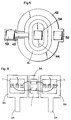
- FET is also of the SOI structure having an N-type silicon layer 10A , a buried oxide layer 20A , and a silicon substrate 30A .
- a P-type well region 11A of a closed loop configuration is diffused in the silicon layer 10A over the full depth thereof so as to leave therearound a peripheral isolated zone 16.
- a P-type source region 12A of the like closed loop configuration is diffused in the top surface of the well region 11A to define the source of FET as well as to define a channel 13A between the source region 12A and a confronting inner periphery of the well region 11A .
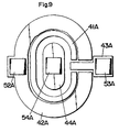
- the above illustrated embodiment discloses the configuration in which the drain region surrounded by the well region, it is equally possible to provide a configuration in which a like well region is formed centrally in the silicon layer and surrounded by a like drain region.
- a peripheral zone around the drain region is electrically connected to a like supporting plate together with the source region.
- a like separator ring may be formed around the drain region to electrically isolate the drain region from the peripheral zone.
Abstract
Description
- 1
- input terminal
- 2
- output terminal
- 3
- control unit
- 4
- light emitting diode
- 5
- photovoltaic cell
- 6
- driver
- 7
- frame
- 8
- chip (photodetector)
- 9
- supporting plate
- 10
- silicon layer
- 11
- well region
- 12
- source region
- 13
- channel
- 14
- drain region
- 15
- insulating stud
- 16
- peripheral zone
- 17
- separator ring
- 18
- land
- 20
- buried oxide layer
- 30
- silicon substrate
- 31
- upper stratum
- 32
- lower stratum
- 33
- cavity
- 34
- recess
- 35
- dielectric layer
- 40
- field oxide layer
- 41
- gate layer
- 42
- source electrode
- 43
- gate electrode
- 44
- drain electrode
- 52
- pad for source electrode
- 53
- pad for gate electrode
- 54
- pad for drain electrode
- 60
- dielectric layer
- 100
- silicon layer
- 101
- drift region
- 102
- drift region
- 111
- well region
- 121
- source region
- 122
- source region
- 131
- channel
- 132
- channel
- 141
- drain region
- 142
- drain region
- 151
- insulator stud
- 152
- insulator stud
- 200
- buried oxide layer
- 300
- silicon substrate
- 341
- recess
- 342
- recess
- 350
- dielectric layer
- 400
- field oxide layer
- 411
- gate layer
- 412
- gate layer
- 421
- source electrode
- 431
- gate electrode
- 432
- gate electrode
- 441
- drain electrode
- 442
- drain electrode
- 521
- pad for source electrode
- 531
- pad for gate electrode
- 541
- pad for drain electrode
Claims (25)
- A solid-state relay having a pair of output terminals for connection with a load to be controlled, said solid-state relay comprising:a control means (3) which gives an electrical energy upon receipt of an input signal;a pair of LDMOSFETs (Lateral Double-diffused Metal Oxide Semiconductor Field Effect Transistors), said LDMOSFETs having individual gates connected commonly to receive said electrical energy to be driven thereby, having individual source connected to each other, and having individual drains connected to said output terminals (2), respectively;at least one supporting plate (9; 9A; 9B) of electrically conductive material mounting thereon said LDMOSFETs;each of said LDMOSFET comprising:a silicon layer (10; 10A; 10B, 100) of a first conductive type having top and bottom surfaces,a drain region (14; 14A; 14B; 141, 142) of said the first conductive type diffused in the top surface of said silicon layer to define said drain of the LDMOSFET;a well region (11; 11A; 11B; 111) of a second conductive type diffused in said silicon layer in a laterally spaced relation from said drain region;a source region (12; 12A; 12B; 121, 122) of the first conductive type diffused within said well region to define a channel extending between said source region and a confronting edge of said well region along the top surface of said silicon layer, said source region defining said source of the LDMOSFET;a drain electrode (44; 44A; 44B; 441,442) being placed on said drain region and electrically connected thereto;a gate electrode electrically connected to a gate layer (41; 41A; 41B; 411, 412) of an electrically conductive material which is placed over said channel through a dielectric layer to define said gate; anda source electrode (42; 42A; 42B; 421) being placed over said source region and electrically connected thereto;characterized in that each of said LDMOSFET is of an SOI (Silicon-On-Insulator) structure which comprises a silicon substrate (30; 30A; 30B, 300), a buried oxide layer (20; 20A; 20B; 200) formed on said silicon substrate, and said silicon layer (10; 10A; 10B; 100) formed on said buried oxide layer, said silicon substrate being mounted on said supporting plate, and wherein said well region extends the full depth of said silicon layer to have a bottom abutted against said buried oxide layer.
- The solid-state relay as set forth in claim 1, wherein one of said source region and said drain region is configured to surround the other of said source region and said drain region within a plane of said silicon layer.
- The solid-state relay as set forth in claim 2, wherein said source region is configured to surround said drain region.
- The solid-state relay as set forth in claim 3, wherein said silicon layer is formed with a peripheral zone (16; 16B) located outwardly of said well region and isolated from said drain region by said well region, said peripheral zone and said drain region being electrically connected commonly to said supporting plate.
- The solid-state relay as set forth in claim 3, wherein a separator ring (17) of a dielectric material surrounds closely said well region, said separator ring being formed in said silicon layer to isolate said well region from a peripheral zone of said silicon layer, said peripheral zone and said drain region being electrically connected commonly to said supporting plate.
- The solid-state relay as set forth in claim 5, wherein at least one of said source electrode and said gate electrode extends laterally over said upper portion of said separator ring (17) from above said well region.
- The solid-state relay as set forth in claim 4, wherein at least one separated land (18) of the second conductive type is diffused in said silicon layer laterally outwardly of said well region in a spaced relation from said well region, at least one of said source electrode and said gate electrode extends over said at least one separator land in a spaced relation thereto from the corresponding one of said source and said channel to define thereat a wiring pad (52B; 53B) for connection with complementary circuit element.
- The solid state relay as set forth in claim 4, wherein a land (18) of the first conductive type is diffused within said well region to extend the full depth of said silicon layer in an electrically isolated relation from said source region, at least one of said source electrode and said gate electrode extends over said separator region in a spaced relation thereto from the corresponding one of said source and said channel to define thereat a wiring pad for connection with complementary circuit element.
- The solid-state relay as set forth in claim 2, wherein the one of said source region and said drain region surrounding the other of said source region and said drain region is electrically connected to said supporting plate of an electrical conductive material so that said supporting plate has the same electrical potential as the one of said well region and said drain region.
- The solid-state relay as set forth in claim 2, wherein said drain region is configured to surround said well region.
- The solid-state relay as set forth in claim 10, wherein said silicon layer is formed with a peripheral zone (16; 16B) located outwardly of said drain region, said peripheral zone and said source region being electrically connected commonly to said supporting plate.
- The solid-state relay as set forth in claim 10, wherein a dielectric separator ring (17) surrounds closely said drain region, said separator ring being formed in said silicon layer to isolate said drain region from a peripheral zone of said silicon layer, said peripheral zone and said source region being electrically connected commonly to said supporting plate.
- The solid-state relay as set forth in claim 1, wherein said source region (12) is electrically connected to said supporting plate (9).
- The solid-state relay as set forth in claim 13, wherein said silicon substrate (30) is formed to have a cavity (33) which extends at the interface with said buried oxide layer and has a width covering said drain region.
- The solid-state relay as set forth in claim 13, wherein said silicon substrate (30B) is formed to have a recess (34) of which bottom is defined by said buried oxide layer and has a width covering said drain region.
- The solid-state relay as set forth in claim 7, wherein said supporting plate is formed separately from said output terminal.
- The solid-state relay as set forth in claim 1, wherein said drain region (14A; 14B) is electrically connected to said supporting plate (9A; 9B).
- The solid state relay as set forth in claim 17, wherein said silicon substrate (30A) is formed with a cavity (33A) which extends at the interface with said buried oxide layer (20A) and has a width covering said source.
- The solid-state relay as set forth in claim 17, wherein said silicon substrate (300) is formed to have a recess (341, 342) of which bottom is defined by said buried oxide layer (200) and has a width covering said source region (121, 122).
- The solid-state relay as set forth in claim 17, wherein said supporting plate (9A) is formed to have said output terminal (2A) as an integral part thereof.
- The solid-state relay as set forth in claim 1, wherein an insulator stud (15; 151, 152) extends from said buried oxide layer (20; 200) through a center of said drain region (14; 141, 142) to project on the top surface of said silicon layer so as to expose said drain region in a annular shape around said stud, said drain electrode extending over said insulator stud with a peripheral portion of the drain electrode being electrically connected to said drain region of the annular shape.
- The solid-state relay as set forth in claim 1, wherein said silicon substrate (30; 30A) comprises a pair of semiconductor stratums (31, 32; 31A, 32A) of opposite conductive type.
- The solid-state relay as set forth in claim 1, wherein a dielectric layer (35; 35A; 35B; 350) is formed on a bottom of the silicon substrate opposite of said buried oxide layer.
- The solid-state relay as set forth in claim 1, wherein said well region (111) is formed in said silicon layer over the full depth thereof in such a manner as to form therein a laterally isolated pair of first and second active zones (101,102) around which a pair of first and second source regions (121,122) are formed respectively in said well region, and wherein a pair of first and second drain regions are formed respectively in said first and second active zones to realize both of said LDMOSFETs in a single device structure,said first and second source regions (121,122) being diffused respectively within said well region (111) so as to be laterally spaced from each other and defining first and second channels (131, 132) each extending between each of said first and second source regions to a confronting edge of each corresponding one of said first and second active zones along the top surface of said silicon layer, said first and second source regions defining first and second sources of the two LDMOSFETs, respectively;said first and second drain regions (141, 142) being diffused respectively within said first and second active zone so as to be isolated from each other by said well region and to define the drains of the two LDMOSFETs, respectively;first and second drain electrodes (441; 442) placed respectively on said first and second drain regions in an electrical connecting relationship therewith;at least one gate electrode (431) being electrically connected to first and second gate layers (411, 412) which are placed over said first and second channels respectively through dielectric layers and define first and second gates of said two LDMOSFETs, respectively;a common source electrode (421) bridging over said first and second source regions and being electrically connected thereto;said first drain (141) being cooperative with said first gate (411) and said first source (121) to make the one of said LDMOSFETs, while said second drain (142) is cooperative with said second gate (412) and said second source (122) to make the other LDMOSFET, andsaid silicon substrate which carries said silicon layer through said buried oxide layer being mounted on said supporting frame with said output terminals being electrically connected respectively to said first and second drains.
- The solid-state relay as set forth in claim 24, wherein said silicon substrate is electrically isolated from said first and second sources and said first and second drains, said output terminals being formed separately from said supporting plate.
Priority Applications (1)
| Application Number | Priority Date | Filing Date | Title |
|---|---|---|---|
| EP02005995A EP1227520B1 (en) | 1997-06-30 | 1998-06-29 | Solid-state relay |
Applications Claiming Priority (12)
| Application Number | Priority Date | Filing Date | Title |
|---|---|---|---|
| JP17430697 | 1997-06-30 | ||
| JP17430697 | 1997-06-30 | ||
| JP174306/97 | 1997-06-30 | ||
| JP314036/97 | 1997-11-14 | ||
| JP314029/97 | 1997-11-14 | ||
| JP31403697 | 1997-11-14 | ||
| JP31403697 | 1997-11-14 | ||
| JP31402997A JP3319999B2 (en) | 1997-11-14 | 1997-11-14 | Semiconductor switch element |
| JP31402997 | 1997-11-14 | ||
| JP352576/97 | 1997-12-22 | ||
| JP35257697 | 1997-12-22 | ||
| JP35257697A JP3513851B2 (en) | 1997-12-22 | 1997-12-22 | Semiconductor device |
Related Child Applications (1)
| Application Number | Title | Priority Date | Filing Date |
|---|---|---|---|
| EP02005995A Division EP1227520B1 (en) | 1997-06-30 | 1998-06-29 | Solid-state relay |
Publications (3)
| Publication Number | Publication Date |
|---|---|
| EP0892438A2 true EP0892438A2 (en) | 1999-01-20 |
| EP0892438A3 EP0892438A3 (en) | 2000-09-13 |
| EP0892438B1 EP0892438B1 (en) | 2007-12-05 |
Family
ID=27474558
Family Applications (2)
| Application Number | Title | Priority Date | Filing Date |
|---|---|---|---|
| EP02005995A Expired - Lifetime EP1227520B1 (en) | 1997-06-30 | 1998-06-29 | Solid-state relay |
| EP98111987A Expired - Lifetime EP0892438B1 (en) | 1997-06-30 | 1998-06-29 | Solid-state relay |
Family Applications Before (1)
| Application Number | Title | Priority Date | Filing Date |
|---|---|---|---|
| EP02005995A Expired - Lifetime EP1227520B1 (en) | 1997-06-30 | 1998-06-29 | Solid-state relay |
Country Status (9)
| Country | Link |
|---|---|
| US (3) | US6211551B1 (en) |
| EP (2) | EP1227520B1 (en) |
| KR (1) | KR100310479B1 (en) |
| CN (1) | CN1156978C (en) |
| CA (1) | CA2241765C (en) |
| DE (2) | DE69840077D1 (en) |
| MY (2) | MY130491A (en) |
| SG (1) | SG67518A1 (en) |
| TW (1) | TW386313B (en) |
Cited By (1)
| Publication number | Priority date | Publication date | Assignee | Title |
|---|---|---|---|---|
| WO2007096210A1 (en) * | 2006-02-22 | 2007-08-30 | Robert Bosch Gmbh | Method and circuit arrangement for simulating fault states in a control device |
Families Citing this family (26)
| Publication number | Priority date | Publication date | Assignee | Title |
|---|---|---|---|---|
| SE9901575L (en) * | 1999-05-03 | 2000-11-04 | Eklund Klas Haakan | semiconductor elements |
| KR100751100B1 (en) * | 1999-09-16 | 2007-08-22 | 코닌클리즈케 필립스 일렉트로닉스 엔.브이. | Semiconductor device |
| US6552396B1 (en) * | 2000-03-14 | 2003-04-22 | International Business Machines Corporation | Matched transistors and methods for forming the same |
| US6614054B1 (en) * | 2000-11-27 | 2003-09-02 | Lg.Philips Lcd Co., Ltd. | Polysilicon thin film transistor used in a liquid crystal display and the fabricating method |
| JP2003101017A (en) * | 2001-09-27 | 2003-04-04 | Mitsubishi Electric Corp | Semiconductor device |
| US6919236B2 (en) * | 2002-03-21 | 2005-07-19 | Advanced Micro Devices, Inc. | Biased, triple-well fully depleted SOI structure, and various methods of making and operating same |
| DE10227310A1 (en) * | 2002-06-19 | 2004-01-15 | Siemens Ag | Semiconductor switching device |
| CN100539184C (en) * | 2004-02-16 | 2009-09-09 | 富士电机电子技术株式会社 | Bi-direction element and manufacture method thereof, semiconductor device |
| JP5157164B2 (en) * | 2006-05-29 | 2013-03-06 | 富士電機株式会社 | Semiconductor device, battery protection circuit and battery pack |
| JP5511124B2 (en) * | 2006-09-28 | 2014-06-04 | セミコンダクター・コンポーネンツ・インダストリーズ・リミテッド・ライアビリティ・カンパニー | Insulated gate semiconductor device |
| JP2008085188A (en) * | 2006-09-28 | 2008-04-10 | Sanyo Electric Co Ltd | Insulated gate semiconductor device |
| KR100840667B1 (en) * | 2007-06-26 | 2008-06-24 | 주식회사 동부하이텍 | Lateral dmos device and fabrication method therefor |
| JP5337470B2 (en) * | 2008-04-21 | 2013-11-06 | セミコンダクター・コンポーネンツ・インダストリーズ・リミテッド・ライアビリティ・カンパニー | Insulated gate semiconductor device |
| JP2010010256A (en) * | 2008-06-25 | 2010-01-14 | Panasonic Electric Works Co Ltd | Semiconductor device |
| US20100127392A1 (en) * | 2008-11-25 | 2010-05-27 | Joe Yang | Semiconductor die |
| US8319255B2 (en) * | 2010-04-01 | 2012-11-27 | Texas Instruments Incorporated | Low side Zener reference voltage extended drain SCR clamps |
| US8524548B2 (en) * | 2011-04-26 | 2013-09-03 | National Semiconductor Corporation | DMOS Transistor with a cavity that lies below the drift region |
| JP5801713B2 (en) * | 2011-12-28 | 2015-10-28 | 株式会社ソシオネクスト | Semiconductor device, manufacturing method thereof, and CAN system |
| EP2869339B1 (en) | 2013-10-31 | 2016-07-27 | Ampleon Netherlands B.V. | Transistor arrangement |
| CN103915505A (en) * | 2014-04-21 | 2014-07-09 | 天津理工大学 | Slot gate and slot source SOILDMOS device |
| CN105374883B (en) * | 2014-08-28 | 2018-06-08 | 旺宏电子股份有限公司 | High voltage device and its manufacturing method |
| US9455339B2 (en) * | 2014-09-09 | 2016-09-27 | Macronix International Co., Ltd. | High voltage device and method for manufacturing the same |
| WO2016187022A1 (en) | 2015-05-15 | 2016-11-24 | Skyworks Solutions, Inc. | Cavity formation in semiconductor devices |
| US9899527B2 (en) * | 2015-12-31 | 2018-02-20 | Globalfoundries Singapore Pte. Ltd. | Integrated circuits with gaps |
| GB2553822B (en) * | 2016-09-15 | 2018-12-26 | Murata Manufacturing Co | DC-DC Converter device |
| TWI829371B (en) * | 2022-09-29 | 2024-01-11 | 車王電子股份有限公司 | solid state relay |
Citations (4)
| Publication number | Priority date | Publication date | Assignee | Title |
|---|---|---|---|---|
| US4864126A (en) * | 1988-06-17 | 1989-09-05 | Hewlett-Packard Company | Solid state relay with optically controlled shunt and series enhancement circuit |
| DE4042334A1 (en) * | 1990-02-27 | 1991-09-05 | Fraunhofer Ges Forschung | Mfg. insulated monocrystalline silicon island - implanting oxygen into highly doped monocrystalline region for forming insulated buried silicon di:oxide layer |
| GB2243485A (en) * | 1990-04-27 | 1991-10-30 | Motorola Gmbh | Semiconductor device contact pads |
| DE4129835A1 (en) * | 1991-09-07 | 1993-03-11 | Bosch Gmbh Robert | POWER ELECTRONIC SUBSTRATE AND METHOD FOR THE PRODUCTION THEREOF |
Family Cites Families (17)
| Publication number | Priority date | Publication date | Assignee | Title |
|---|---|---|---|---|
| JPS63278375A (en) * | 1987-05-11 | 1988-11-16 | Nec Corp | Semiconductor integrated circuit device |
| US5126827A (en) * | 1991-01-17 | 1992-06-30 | Avantek, Inc. | Semiconductor chip header having particular surface metallization |
| US5138177A (en) * | 1991-03-26 | 1992-08-11 | At&T Bell Laboratories | Solid-state relay |
| JP2654268B2 (en) * | 1991-05-13 | 1997-09-17 | 株式会社東芝 | How to use semiconductor devices |
| US5286995A (en) * | 1992-07-14 | 1994-02-15 | Texas Instruments Incorporated | Isolated resurf LDMOS devices for multiple outputs on one die |
| JPH06268247A (en) * | 1993-03-15 | 1994-09-22 | Matsushita Electric Works Ltd | Optically coupled semiconductor relay |
| US5378912A (en) * | 1993-11-10 | 1995-01-03 | Philips Electronics North America Corporation | Lateral semiconductor-on-insulator (SOI) semiconductor device having a lateral drift region |
| US5382818A (en) * | 1993-12-08 | 1995-01-17 | Philips Electronics North America Corporation | Lateral semiconductor-on-insulator (SOI) semiconductor device having a buried diode |
| JPH07211911A (en) | 1994-01-19 | 1995-08-11 | Nippon Telegr & Teleph Corp <Ntt> | Insulated gate type field effect transistor |
| US5874768A (en) * | 1994-06-15 | 1999-02-23 | Nippondenso Co., Ltd. | Semiconductor device having a high breakdown voltage |
| JPH08335684A (en) * | 1995-06-08 | 1996-12-17 | Toshiba Corp | Semiconductor device |
| US5828112A (en) * | 1995-09-18 | 1998-10-27 | Kabushiki Kaisha Toshiba | Semiconductor device incorporating an output element having a current-detecting section |
| TW360982B (en) * | 1996-01-26 | 1999-06-11 | Matsushita Electric Works Ltd | Thin film transistor of silicon-on-insulator type |
| JP3575908B2 (en) * | 1996-03-28 | 2004-10-13 | 株式会社東芝 | Semiconductor device |
| JP3082189B2 (en) | 1996-05-22 | 2000-08-28 | 横河電機株式会社 | Semiconductor relay |
| US5760473A (en) * | 1996-06-25 | 1998-06-02 | Brush Wellman Inc. | Semiconductor package having a eutectic bonding layer |
| US5981983A (en) * | 1996-09-18 | 1999-11-09 | Kabushiki Kaisha Toshiba | High voltage semiconductor device |
-
1998
- 1998-06-26 US US09/105,464 patent/US6211551B1/en not_active Expired - Lifetime
- 1998-06-26 SG SG1998001526A patent/SG67518A1/en unknown
- 1998-06-26 CA CA002241765A patent/CA2241765C/en not_active Expired - Fee Related
- 1998-06-29 DE DE69840077T patent/DE69840077D1/en not_active Expired - Lifetime
- 1998-06-29 EP EP02005995A patent/EP1227520B1/en not_active Expired - Lifetime
- 1998-06-29 TW TW087110440A patent/TW386313B/en not_active IP Right Cessation
- 1998-06-29 DE DE69838805T patent/DE69838805T2/en not_active Expired - Lifetime
- 1998-06-29 EP EP98111987A patent/EP0892438B1/en not_active Expired - Lifetime
- 1998-06-30 MY MYPI20022455A patent/MY130491A/en unknown
- 1998-06-30 MY MYPI98002980A patent/MY118511A/en unknown
- 1998-06-30 KR KR1019980025687A patent/KR100310479B1/en not_active IP Right Cessation
- 1998-06-30 CN CNB981026826A patent/CN1156978C/en not_active Expired - Fee Related
-
2000
- 2000-11-13 US US09/709,582 patent/US6580126B1/en not_active Expired - Fee Related
- 2000-11-13 US US09/709,528 patent/US6373101B1/en not_active Expired - Fee Related
Patent Citations (4)
| Publication number | Priority date | Publication date | Assignee | Title |
|---|---|---|---|---|
| US4864126A (en) * | 1988-06-17 | 1989-09-05 | Hewlett-Packard Company | Solid state relay with optically controlled shunt and series enhancement circuit |
| DE4042334A1 (en) * | 1990-02-27 | 1991-09-05 | Fraunhofer Ges Forschung | Mfg. insulated monocrystalline silicon island - implanting oxygen into highly doped monocrystalline region for forming insulated buried silicon di:oxide layer |
| GB2243485A (en) * | 1990-04-27 | 1991-10-30 | Motorola Gmbh | Semiconductor device contact pads |
| DE4129835A1 (en) * | 1991-09-07 | 1993-03-11 | Bosch Gmbh Robert | POWER ELECTRONIC SUBSTRATE AND METHOD FOR THE PRODUCTION THEREOF |
Non-Patent Citations (3)
| Title |
|---|
| PATENT ABSTRACTS OF JAPAN vol. 1995, no. 11, 26 December 1995 (1995-12-26) & JP 07 211911 A (NIPPON TELEGR & TELEPH CORP), 11 August 1995 (1995-08-11) * |
| PAUL A K ET AL: "HIGH VOLTAGE LDMOS TRANSISTORS IN SUB-MICRON SOI FILMS" PROCEEDINGS OF THE INTERNATIONAL SYMPOSIUM ON POWER SEMICONDUCTOR DEVICES AND IC'S (ISPSD),US,NEW YORK, IEEE, vol. SYMP. 8, 1996, pages 89-92, XP000598404 ISBN: 0-7803-3107-9 * |
| YING-KEUNG LEUNG ET AL: "Self-heating effect in lateral DMOS on SOI" PROCEEDINGS OF THE 7TH INTERNATIONAL SYMPOSIUM ON POWER SEMICONDUCTOR DEVICES AND ICS, ISPSD 95 (IEEE CAT. NO.95CH35785), PROCEEDINGS OF INTERNATIONAL SYMPOSIUM ON POWER SEMICONDUCTOR DEVICES AND IC S: ISPSD 95, YOKOHAMA, JAPAN, 23-25 MAY 1995, pages 136-140, XP002141828 1995, Tokyo, Japan, Inst. Electr. Eng. Japan, Japan ISBN: 0-7803-2618-0 * |
Cited By (2)
| Publication number | Priority date | Publication date | Assignee | Title |
|---|---|---|---|---|
| WO2007096210A1 (en) * | 2006-02-22 | 2007-08-30 | Robert Bosch Gmbh | Method and circuit arrangement for simulating fault states in a control device |
| US8589139B2 (en) | 2006-02-22 | 2013-11-19 | Robert Bosch Gmbh | Method and circuit configuration for simulating fault states in a control unit |
Also Published As
| Publication number | Publication date |
|---|---|
| KR100310479B1 (en) | 2001-11-30 |
| MY130491A (en) | 2007-06-29 |
| EP1227520A3 (en) | 2003-06-18 |
| MY118511A (en) | 2004-11-30 |
| US6580126B1 (en) | 2003-06-17 |
| US6373101B1 (en) | 2002-04-16 |
| DE69840077D1 (en) | 2008-11-13 |
| SG67518A1 (en) | 1999-09-21 |
| CN1156978C (en) | 2004-07-07 |
| CA2241765A1 (en) | 1998-12-30 |
| EP0892438A3 (en) | 2000-09-13 |
| KR19990007497A (en) | 1999-01-25 |
| DE69838805D1 (en) | 2008-01-17 |
| US6211551B1 (en) | 2001-04-03 |
| EP1227520B1 (en) | 2008-10-01 |
| TW386313B (en) | 2000-04-01 |
| CN1222789A (en) | 1999-07-14 |
| CA2241765C (en) | 2001-08-28 |
| EP0892438B1 (en) | 2007-12-05 |
| DE69838805T2 (en) | 2008-03-20 |
| EP1227520A2 (en) | 2002-07-31 |
Similar Documents
| Publication | Publication Date | Title |
|---|---|---|
| CA2241765C (en) | Solid-state relay | |
| KR100643831B1 (en) | Semiconductor device | |
| US6573144B2 (en) | Method for manufacturing a semiconductor device having lateral MOSFET (LDMOS) | |
| TWI552310B (en) | Semiconductor device | |
| US7427792B2 (en) | Power transistor including a leadframe and a semiconductor chip arranged on the leadframe | |
| KR20010015835A (en) | Semiconductor device | |
| JP2003017701A (en) | Semiconductor device | |
| US20120161128A1 (en) | Die package | |
| JP2003007843A (en) | Semiconductor device | |
| JP3509552B2 (en) | Semiconductor device | |
| US8502307B2 (en) | Vertical power semiconductor carrier having laterally isolated circuit areas | |
| US20040129864A1 (en) | Photovoltaic solid state relay | |
| JP4447768B2 (en) | Field MOS transistor and semiconductor integrated circuit including the same | |
| KR20140131378A (en) | Power field effect transistor | |
| EP0323843A2 (en) | Multi-output vertical type power semiconductor device | |
| CN108233910B (en) | Electronic circuit | |
| US6809393B1 (en) | Level shifter | |
| KR100312467B1 (en) | Semiconductor ic device | |
| US20230290879A1 (en) | Semiconductor device | |
| JP3142749B2 (en) | Semiconductor device | |
| JP3513851B2 (en) | Semiconductor device | |
| JPH104143A (en) | Semiconductor integrated circuit | |
| EP1074050A1 (en) | Insulated-gate field-effect semiconductor device | |
| JP2001168336A (en) | Low-capacitance mosfet and semiconductor relay device using it | |
| JP2001244422A (en) | Semiconductor device |
Legal Events
| Date | Code | Title | Description |
|---|---|---|---|
| PUAI | Public reference made under article 153(3) epc to a published international application that has entered the european phase |
Free format text: ORIGINAL CODE: 0009012 |
|
| AK | Designated contracting states |
Kind code of ref document: A2 Designated state(s): DE FR GB IT NL |
|
| AX | Request for extension of the european patent |
Free format text: AL;LT;LV;MK;RO;SI |
|
| PUAL | Search report despatched |
Free format text: ORIGINAL CODE: 0009013 |
|
| RIC1 | Information provided on ipc code assigned before grant |
Free format text: 7H 01L 27/12 A, 7H 01L 27/088 B, 7H 03K 17/785 B |
|
| AK | Designated contracting states |
Kind code of ref document: A3 Designated state(s): AT BE CH CY DE DK ES FI FR GB GR IE IT LI LU MC NL PT SE |
|
| AX | Request for extension of the european patent |
Free format text: AL;LT;LV;MK;RO;SI |
|
| 17P | Request for examination filed |
Effective date: 20001023 |
|
| AKX | Designation fees paid |
Free format text: DE FR GB IT NL |
|
| 17Q | First examination report despatched |
Effective date: 20011026 |
|
| RIN1 | Information on inventor provided before grant (corrected) |
Inventor name: MIYAMOTO, YASUNORI Inventor name: YOSHIDA, TAKESHI Inventor name: SHIRAI, YOSHIFUMI Inventor name: HAYASAKI, YOSHIKI Inventor name: KISHIDA, TAKASHI Inventor name: SUZUKI, YUJI Inventor name: TAKANO, HITOMICHI Inventor name: SUZUMURA, MASAHIKO |
|
| 17Q | First examination report despatched |
Effective date: 20011026 |
|
| RIC1 | Information provided on ipc code assigned before grant |
Ipc: H03K 17/785 20060101ALI20070427BHEP Ipc: H01L 27/088 20060101ALI20070427BHEP Ipc: H01L 27/12 20060101ALI20070427BHEP Ipc: H01L 29/06 20060101ALI20070427BHEP Ipc: H01L 29/78 20060101AFI20070427BHEP |
|
| GRAP | Despatch of communication of intention to grant a patent |
Free format text: ORIGINAL CODE: EPIDOSNIGR1 |
|
| GRAS | Grant fee paid |
Free format text: ORIGINAL CODE: EPIDOSNIGR3 |
|
| GRAA | (expected) grant |
Free format text: ORIGINAL CODE: 0009210 |
|
| AK | Designated contracting states |
Kind code of ref document: B1 Designated state(s): DE FR GB IT NL |
|
| REG | Reference to a national code |
Ref country code: GB Ref legal event code: FG4D |
|
| REF | Corresponds to: |
Ref document number: 69838805 Country of ref document: DE Date of ref document: 20080117 Kind code of ref document: P |
|
| ET | Fr: translation filed | ||
| PLBE | No opposition filed within time limit |
Free format text: ORIGINAL CODE: 0009261 |
|
| STAA | Information on the status of an ep patent application or granted ep patent |
Free format text: STATUS: NO OPPOSITION FILED WITHIN TIME LIMIT |
|
| 26N | No opposition filed |
Effective date: 20080908 |
|
| PGFP | Annual fee paid to national office [announced via postgrant information from national office to epo] |
Ref country code: NL Payment date: 20120626 Year of fee payment: 15 Ref country code: DE Payment date: 20120627 Year of fee payment: 15 |
|
| PGFP | Annual fee paid to national office [announced via postgrant information from national office to epo] |
Ref country code: FR Payment date: 20120619 Year of fee payment: 15 Ref country code: GB Payment date: 20120627 Year of fee payment: 15 |
|
| PGFP | Annual fee paid to national office [announced via postgrant information from national office to epo] |
Ref country code: IT Payment date: 20120619 Year of fee payment: 15 |
|
| REG | Reference to a national code |
Ref country code: NL Ref legal event code: V1 Effective date: 20140101 |
|
| GBPC | Gb: european patent ceased through non-payment of renewal fee |
Effective date: 20130629 |
|
| REG | Reference to a national code |
Ref country code: DE Ref legal event code: R119 Ref document number: 69838805 Country of ref document: DE Effective date: 20140101 |
|
| REG | Reference to a national code |
Ref country code: FR Ref legal event code: ST Effective date: 20140228 |
|
| PG25 | Lapsed in a contracting state [announced via postgrant information from national office to epo] |
Ref country code: DE Free format text: LAPSE BECAUSE OF NON-PAYMENT OF DUE FEES Effective date: 20140101 Ref country code: GB Free format text: LAPSE BECAUSE OF NON-PAYMENT OF DUE FEES Effective date: 20130629 Ref country code: NL Free format text: LAPSE BECAUSE OF NON-PAYMENT OF DUE FEES Effective date: 20140101 |
|
| PG25 | Lapsed in a contracting state [announced via postgrant information from national office to epo] |
Ref country code: IT Free format text: LAPSE BECAUSE OF NON-PAYMENT OF DUE FEES Effective date: 20130629 Ref country code: FR Free format text: LAPSE BECAUSE OF NON-PAYMENT OF DUE FEES Effective date: 20130701 |