EP0887752A2 - Microstrip gas chamber high-speed data acquisition system and method of measuring samples by use of the system - Google Patents
Microstrip gas chamber high-speed data acquisition system and method of measuring samples by use of the system Download PDFInfo
- Publication number
- EP0887752A2 EP0887752A2 EP98110642A EP98110642A EP0887752A2 EP 0887752 A2 EP0887752 A2 EP 0887752A2 EP 98110642 A EP98110642 A EP 98110642A EP 98110642 A EP98110642 A EP 98110642A EP 0887752 A2 EP0887752 A2 EP 0887752A2
- Authority
- EP
- European Patent Office
- Prior art keywords
- signals
- gas chamber
- particle
- strips
- incident
- Prior art date
- Legal status (The legal status is an assumption and is not a legal conclusion. Google has not performed a legal analysis and makes no representation as to the accuracy of the status listed.)
- Granted
Links
Images


Classifications
-
- G—PHYSICS
- G01—MEASURING; TESTING
- G01T—MEASUREMENT OF NUCLEAR OR X-RADIATION
- G01T1/00—Measuring X-radiation, gamma radiation, corpuscular radiation, or cosmic radiation
- G01T1/29—Measurement performed on radiation beams, e.g. position or section of the beam; Measurement of spatial distribution of radiation
- G01T1/2914—Measurement of spatial distribution of radiation
- G01T1/2921—Static instruments for imaging the distribution of radioactivity in one or two dimensions; Radio-isotope cameras
- G01T1/2935—Static instruments for imaging the distribution of radioactivity in one or two dimensions; Radio-isotope cameras using ionisation detectors
Definitions
- the present invention relates to an imaging microstrip gas chamber (MSGC) high-speed data acquisition system and to a method of measuring samples by use of the system.
- MSGC imaging microstrip gas chamber
- MSGC microstrip gas chamber
- One conventionally-used method for data acquisition is a charge distribution method in which all signal lines are connected through resistors disposed between adjacent signal lines, and the heights of electrical signal pulses from opposite ends of the lines are measured to obtain a position of an incident particle on the basis of the ratio between the heights of electrical signal pulses.
- a time interval of a few hundred nsec. to a few ⁇ sec. has been required to convert the height of a pulse to a high accuracy (8 bits or more) digital signal for computation.
- Reading outputs from all signal lines is considered a most reliably and high-speed data acquisition method.
- signal outputs for each of vertical and horizontal directions must be read out together with their timings. Therefore, an electronic apparatus for such an operation becomes huge.
- the inventors of the present invention have employed a method in which outputs of all signal lines are input to a timing digital converters (TDC) after being converted into binary signals (on/off signals), and all the outputs from the TDC are read out by a computer, where a position of an incident signal is obtained by means of software.
- TDC timing digital converters
- the amount of data to be transferred from the TDC to the computer is huge, the transfer requires a prolonged period of time, and the speed of the processing performed in the computer cannot be increased. Therefore, the data acquisition capability of the conventional method is limited to ⁇ 1000 cps.
- the MSGC is a gas detector having a very narrow inter-signal line pitch of 200 ⁇ m, the MSGC has the following features:
- the performance of the MSGC is sufficient to satisfy the demand of a new synchrotron radiation experiment.
- the incident rate capacity of the conventional data acquisition system is far below the above-described desired capacity. Therefore, there must be constructed a high-speed data acquisition system which can fully utilize the capacity of the MSGC; i.e., which can process/record X-ray events occurring at a rate of 10 6 cps or higher.
- an object of the present invention is to provide an imaging microstrip gas chamber (MSGC) high-speed data acquisition system which can process at high speed a large number of output signals of an imaging microstrip gas chamber.
- MSGC imaging microstrip gas chamber
- Another object of the present invention is to provide a method of measuring samples by use of the high-speed data acquisition system.
- the present invention provides a two-dimensional microstrip gas chamber high-speed data acquisition system comprising: discrimination circuits for binary conversion of signals from anode strips and back strips of a two-dimensional microstrip gas chamber; signal synchronizing circuits for converting binary asynchronous signals output from the discrimination circuits into clock-synchronized signals; data encoder circuits connected to the signal synchronizing circuits; an incident-particle hit judgment circuit connected to the data encoder circuits and operating such that when, among a plurality of input signal lines for each of the vertical and horizontal axes, a plurality of adjacent signal lines receive signals at the same timing, the incident-particle hit judgment circuit outputs a value corresponding to a signal line at the center of the adjacent signal lines, and when separated signal lines receive signals at the same timing, the incident-particle hit judgment circuit ignores the signals; a storage device connected to the incident-particle hit judgment circuit and adapted to store, for each event, the vertical and horizontal coordinates of an incident particle, the timing of incidence of the particle
- an amplifier is connected to each of the anode strips and back strips of the two-dimensional microstrip gas chamber, and an output signal from the amplifier is input to the corresponding discrimination circuit.
- the data encoder circuit comprises an upper priory encoders, a lower priority encoders, and an adding circuit, wherein the values of signals transmitted through upper and lower signal lines are obtained through use of the upper priority encoder and the lower priority encoder, and the mean value of the thus-obtained values is used for calculation of the coordinates of an incident particle.
- the two-dimensional coordinates of an incident particle can be obtained accurately.
- each of the signal synchronizing circuits, the data encoder circuits, and the incident-particle hit judgment circuit is formed of a CPLD (Complex Programmable Logic Device).
- the size of the data acquisition system can be decreased.
- the two-dimensional microstrip gas chamber comprises a substrate formed of organic thin film having elasticity; anode strips and cathode strips formed on the substrate to be alternately arranged in parallel; a high voltage source for applying high voltage between the anode strips and the cathode strips; back strips formed on the lower face of the substrate to intersect the anode strips and the cathode strips; a drift plane disposed a predetermined distance away from the substrate; and a gas source for supplying a gas to be passed through a space between the surface of the substrate and the drift plane, wherein electron amplification effect of the gas is caused, and signals regarding an X-ray or particle are extracted for simultaneous measurement of the two-dimensional coordinates of the X-ray or particle.
- the opposite edge portions of each of the cathode strips are preferably coated with organic thin film having elasticity.
- the organic thin film having elasticity is preferably polyimide film.
- the surface area can be increased, so that a uniform image can be drawn on a flexible surface.
- the surface of the substrate is preferably coated with organic titanium in order to control the surface resistance.
- charging at the substrate surface can be suppressed through control of the surface resistance of the substrate.
- an IC package is preferably provided under the back strips, wherein the IC package is an LSI high-density package.
- a compact and highly integrated two-dimensional MSGC can be provided. Further, a large two-dimensional MSGC having a large effective area of, for example, 10 cm x 10 cm can be designed. This two-dimensional MSGC having about 1000 channels can be mounted directly on a circuit board, and amplifiers can be disposed thereon.
- the back strips are connected to first bonding pads on the top surface of the substrate through fine through-holes; the edge portion of the IC package is raised to form a wall portion; second bonding pads are formed on the top surface of the wall portion; and the first and second bonding pads are connected with each other through use of bonding wires.
- the above-described structure increases the degree of integration while facilitating wiring work. Further, above-described structure allows use of a various kinds of microelectronics techniques generally employed in the semiconductor field, such as formation of through-holes and micro resistors and capacitors.
- the two-dimensional microstrip gas chamber having the above-described structure is preferably used as an X-ray imaging detector by use of X-ray irradiation.
- an X-ray imaging detector that provides stable operation even under strong X-ray irradiation. That is, proper operation is possible even when the level of X-ray irradiation is as high as 2 x 10 7 Hz/mm 2 . Further, there can be obtained very clear images having a high position resolution of 100 ⁇ m or better.
- the present invention also provides a method of measuring a sample, comprising the step of constructing a microstrip gas chamber high-speed data acquisition system including: discrimination circuits for binary conversion of signals from anode strips and back strips of a two-dimensional microstrip gas chamber; signal synchronizing circuits for converting binary asynchronous signals output from the discrimination circuits into clock-synchronized signals; data encoder circuits connected to the signal synchronizing circuits; an incident-particle hit judgment circuit connected to the data encoder circuits and operating such that when among a plurality of input signal lines for each of the vertical and horizontal axes a plurality of adjacent signal lines receive signals at the same timing, the incident-particle hit judgment circuit outputs a value corresponding to a signal line at the center of the adjacent signal lines, and when separated signal lines receive signals at the same timing, the incident-particle hit judgment circuit ignores the signals; a storage device connected to the incident-particle hit judgment circuit and adapted to store, for each event, the vertical and horizontal coordinates of an incident particle, the timing
- the measuring method of the present invention enables directly observation of the process of fast changes in a moving sample through radiation of an X-ray beam and X-ray diffraction, thereby contributing the study of the sample.
- the sample is preferably a solid crystal, and the process of changes in the structure of the solid crystal is directly observed.
- the process of change in the sample is preferably measured at intervals of 1/1000 second or less.
- the process of change in the sample can be measured with high time resolution.
- the measuring method of the present invention is used to observe an excited state of the solid crystal.
- the excited state of the solid crystal can be measured quickly and precisely.
- measurement is performed in accordance with a rotation continuous photograph method; and the position of an X-ray resulting from X-ray diffraction during the measurement and the timing of the X-ray diffraction are measured so as to determine a three-dimensional crystalline structure.
- the process of change in a three-dimensional crystal can be measured quickly and precisely.
- the vertical coordinate and the horizontal coordinate of the incident position of a particle are obtained from the digital signals, and a two-dimensional position coordinates are determined on the basis of the vertical and horizontal coordinates measured at the same timing.
- a two-dimensional position coordinates are accumulated in a dedicated storage device (memory). Since the storage device can be accessed from the computer, acquired data can be processed in real time.
- the present invention enables acquisition of data regarding 10 million events per second, which amount is 5000 or more times that of the conventional system. This enables the capture of changes with time in X-ray or particle images, so that the images can be captured as moving images.
- the present system can collect signals output from the MSGC at high speed and can cause the directly connected computer to analyze the collected signals.
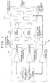
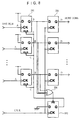
- Fig. 1 shows a block diagram of an MSGC data acquisition system according to the embodiment of the present invention.
- the MSGC data acquisition system of the present invention is generally composed of a two-dimensional MSGC, preamplifiers discriminators, signal synchronizing circuits, data encoders (for encoding particle incident positions), an incident-particle hit judgment circuit, a large capacity storage device, and a computer.
- a motherboard 101 on a motherboard 101 are mounted the two-dimensional MSGC (hereinafter simply referred to as MSGC) 102, preamplifiers/discriminators 103 and 104, and a preamplifier 105.
- MSGC two-dimensional MSGC
- a first signal synchronizing circuit 111 for processing output signals (signals under the ECL standard) from anodes of the MSGC 102
- a second signal synchronizing circuit 112 for processing output signals (signals under the ECL standard) from back strips of the MSGC 102
- a first encoder 113 connected to the first signal synchronizing circuit 111
- a second encoder 114 connected to the second signal synchronizing circuit 112
- the incident-particle hit judgment circuit 115 the large capacity storage device 116
- the computer 117 the computer 117.
- the cathodes of the MSGC 102 are connected to the storage device 116 via the preamplifier 105 and an analog-to-digital converter (ADC) 106.
- ADC analog-to-digital converter
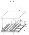
- Fig. 2 shows an exploded perspective view of the MSGC according to the embodiment of the present invention.
- Figs. 3(a) and 3(b) are views showing coated cathode edges, wherein Fig. 3(a) is a partial plan view of the cathodes, and Fig. 3(b) is an enlarged view of a portion indicated by symbol A in Fig 3(a).
- the two-dimensional MSGC 102 shown in Figs. 2, 3(a), and 3(b) has an effective area of 10 cm x 10 cm.
- Numeral 1 denotes a substrate formed of a polyimide thin film having a thickness of about 17 ⁇ m.
- Numeral 2 denotes anode strips formed on the substrate 1.
- Each of the anode strips 2 is formed of 1 ⁇ m-thick Au/Ti film and has a width D 2 of about 10 ⁇ m.
- Numeral 3 denotes cathode strips.
- Each of the cathode strips 3 is formed of 1 ⁇ m-thick Au/Ti film and has a width D 3 of about 100 ⁇ m.
- the anode strips 2 and the cathode strips 3 are arranged alternately such that the pitch D 4 of the anode strips 2 is about 200 ⁇ m.
- Numeral 4 denotes a base substrate formed of ceramic
- numeral 5 denotes back strips formed on the base substrate 4 to be located under the substrate 1.
- Each of the back strips 5 is formed of 1 ⁇ m-thick Au/Ti film and has a width D 5 of about 180 ⁇ m.
- a drift plane 6 is disposed above the element having the above-described structure such that the distance D 1 between the element and the drift plane 6 becomes 1 cm.
- a chamber through which flows gas including argon and ethane.
- gas including argon and ethane In general, a rare gas having a large atomic weight and suppressing discharge is used for the MSGC.
- a mixed gas of methane, ethane, carbon dioxide, and the like may be used.
- Numeral 7 denotes amplifiers.
- the substrate 1 is formed of polyimide thin film of about 17 ⁇ m thick, and the back strips 5 are formed on the base substrate 4 to be located under the polyimide thin film, two-dimensional readout can be performed through use of signals induced in the back strips 5. That is, use of the polyimide substrate 1 enables simultaneous measurement of two-dimensional coordinates. Since polyimide has a high degree of flexibility and elasticity, there can be manufactured a polyimide substrate having a large surface that is completely flat and smooth.
- polyimide film can be formed in a desired shape with an accuracy on the order of 1 micron.
- a guarding mask for protecting the anode strips and through holes are formed by use of the MCM technique.
- the size of the two-dimensional MSGC can be increased to 20 cm x 20 cm or larger.
- the substrate is formed of polyimide.
- the MSGC of the present invention can be constructed from other organic material having elasticity. Examples of such organic material having elasticity include polyamide, polyamideimide, polysulfone, and polycarbonate, and among organic materials polyimide is preferred.
- the elastic organic film can have a thickness of 5 - 100 ⁇ m, a thickness of 10 - 30 ⁇ m is preferred.
- the MSGC 102 is designed such that for each of the X and Y directions, signals are extracted at a very small pitch of 200 ⁇ m. Therefore, when the MSGC has a size of 5 cm x 5 cm, 500 or more signal lines must be connected to a corresponding number of amplifiers 7.
- the MSGC is packaged on an LSI high density package in order to facilitate and improve the connection between the MSGC and a circuit board.
- the coordinate values representing the position of an X-ray or a particle are determined through use of signals from the back strips 5 and the anode strips 2.
- the cathode strips 3 are used for measurement of energy loss of a particle in a MSGC gas. In order to reduce the number of readout channels, for readout purposes the cathode strips 3 are divided into groups each containing ten cathode strips.
- the signals are extracted from an IC package 11 (see Fig. 5) containing the MSGC.
- Figs. 4(a) and 4(b) are views showing the structure of a PGA package on which is mounted a two-dimensional MSGC of 5 cm x 5 cm, wherein Fig. 4(a) is a perspective view of the package, while Fig. 4(b) is a bottom view of the package.
- the IC package 11 is formed of ceramic, and 541 strips are provided on the bottom surface at a pitch of 0.1 inches. All of 254 anode strips, 255 back strips, and 17 groups of cathodes are connected to the IC package by means of gold wire bonding. Therefore, no wires are required to be connected directly to the plate of the MSGC 102.
- Fig. 5 is a partial sectional view of the IC package on which is mounted the two-dimensional MSGC.
- the same portions as those shown in Fig. 3 are denoted by identical numerals, and descriptions thereof will be omitted.
- numeral 4 denotes a base substrate; and numeral 10 denotes a first bonding pad formed on the substrate 1 and connected to the corresponding back strip 5 via a fine through-hole 1A.
- the edge of the IC package 11 is raised to form a wall portion 11A, and a second bonding pad 13 is formed on the top surface of the wall portion 11A.
- the second bonding pad 13 is connected to the first bonding pad 10 through use of a bonding wire 14.
- a measured crosstalk between adjacent strips is about 5%, and therefore does not cause a problem in relation to digital readout of data from the MSGC of the present invention.
- the MSGC 102 When the MSGC 102 is used as an X-ray imaging device, as shown in Fig. 2, the MSGC 102 must have electrodes other than the anode strips 2.
- the MSGC 102 according to the present embodiment has three kinds of electrodes; i.e., the cathode strips 3, the drift plane 6, and the back strips 5.
- the cathodes strips 3 can induce strong signals, the induced signals have a long rising time of about 200 nsec., and the cathode strips 3 run in parallel to the anode strips 2.
- drift plate drift plate
- induction speed of such a signal is very slow (about 10 ⁇ m).
- back strips back strips
- the height and shape of a pulse (induced signal) depend on the geometric structure of the electrode of the MSCG, as well as on the thickness and material of the substrate, it is clear that high speed signals can be obtained from the back strips.
- the MSGC 102 shown in Fig. 1 has 512 anode strips, 512 back strips, and cathodes.
- Very feeble signal pluses output from the MSGC 102 are amplified by wave-shaping/preamplifiers (LeCroy MQS 104).
- the pulses output from the wave-shaping/preamplifiers have a pulse width of 30 nsec. or less.
- the output pluses are fed to the preamplifiers discriminators (LeCroy MVL407) 103 and 104, and discrimination signals conforming to the ECL (Emitter-Coupled Logic) standard are output from the preamplifiers discriminators 103 and 104.
- Each of ICs used in these circuits includes circuits for 4 channels. In the present system, cards each containing the preamplifiers discriminators 103 and 104 for 64 channels are mounted on the motherboard 101 in order to reduce the size of the apparatus.
- the outputs under the ECL standard are fed to the data acquisition system via a multi-conductor signal cable.
- the data acquisition system can be divided into the encoders 113 and 114 for locating the position of a signal ray on the basis of the fed signals, the incident-particle hit judging circuit 115, and the large capacity storage device 116 for storing obtained position information.
- the computer i.e., control CPU; Force CPU-7V, SUN compatible
- the CPU 117 is connected to a high-speed network (presently, 100 Mbps) in order to allow other computers to analyze data obtained by the MSGC 102.
- the gas amplification factor of the MSGC is generally 500, which is very small compared with that of other gas amplifiers in which wires are used.
- an amount of charge induced on the MSGC due to incidence of an X-ray of about 8 keV is about 1.0 - 2.0 x 10 -14 C.
- the signals in order to separate signals having a frequency of 10 MHz or higher, the signals must be shaped to have a width of about 20 nsec. Further, a huge number of signal lines must be handled. In order to meet these requirements, there must be used high-speed, highly integrated preamplifiers having a large amplification factor.
- the preamplifiers used in the present embodiment are MQS 104A (product of LeCroy Corp.), which was originally developed for wire chambers.
- the ICs constituting preamplifiers has a charge amplification factor of 30 mV/fC.
- the wave-shaper included in the IC shapes the output waveform to have a half-value width of 20 nsec. Since four circuits are included in each IC of about 1 cm x 1 cm, the preamplifiers can be formed to be relatively compact.
- the output signals obtained form the anodes and the back electrodes are all converted into binary signals through use of comparators.
- MVL 407S of LeCroy is used for the comparators.
- Each of the ICs constituting the comparators includes 4 circuits. Since the MVL 407S provides an ECL differential output, it can drive a cable of about a few meters in length without use of an additional circuit.
- the RMS resolution can be increased up to 30 ⁇ m.
- the RMS resolution can be increased up to about 60 ⁇ m even when there is employed a method based on binary value readout.
- preamplifier discriminator integrated circuit boards that can be mounted vertically on the motherboard which carries the detector.
- 16 MQS104A chips, 16 MVL407S chips (both surface-mount type) and other integrated-type circuit components are mounted on front and rear surfaces of each of 8 layered printed circuit boards each having a size of about 15 cm x 15 cm, thereby realizing circuits for 64 channels. Connection between the printed circuit boards and the motherboard is performed through use of 120-pin connectors disposed at 1/20-inch intervals. From these connectors are received electrical power for circuits and discrimination voltage, as well as signals.
- each signal is output in the form of an ECL differential output, two signal lines must be used for each signal.
- two 68-pin half-pitch connectors are mounted in order to allow output of signals for 64 channels.
- MSGC MSGC of 10 cm x 10 cm, since the number of outputs including outputs from the anodes and the back electrodes is 1024, 16 preamplifier discriminator boards must be used.
- the function of the data encoders is to convert the outputs from the signal lines into the coordinate values of the incident particle.
- this function is realized by means of hardware in order to speed up the operation of the MSGC data acquisition system. This feature constitutes the core of the system.
- the first and second encoders 113 and 114 are mounted on boards of VME-9U, each of which has a double-width front panel. On the front panels are disposed eight connectors for connection with cables extended from the above-described preamplifiers/wave-height discriminators 103 and 104. Thus, input of signals for 256 channels is enabled. In order to read out data from the MSGC of 10 cm x 10 cm, for each of the X- and Y-axis directions, 512 signals must be input. Therefore, two encoder boards for each of the X- and Y-axis directions; i.e., four encoder boards in total, are required.
- the ECL differential signal is converted into a TTL (Transistor-Transistor Logic) signal, and is then fed to an encoder circuit formed of a CPLD (Complex Programmable Logic Device).
- the CPLD is formed through integration of conventional PLDs.
- EPM7192 and EPM7256 products of Altera Corp. are used. Since the input signals are asynchronous, a signal synchronizing circuit is disposed in the first stage of the encoder circuit in order to allow subsequent signal processing to be performed in synchronization with clocks.
- CPLDs are used for each board. Two of the CPLDs are used for signal synchronization, while the remaining one is used for coordinate encoding. From the encoder circuit are output coordinates of an incident particle, a signal (HIT) indicating the presence/absence of an event in each clock period, a signal (DUP) for invalidating signals when the signals are simultaneously input from the input lines separated away from each other, and a signal indicating that an event causes signals to be output from several adjacent signal lines. These signals are all output to a J3 connector of the VME bus and then transferred to a memory board.
- HIT signal
- DUP signal
- the signal input is used for a clock input signal of a flip-flop in order to recognize an edge of the signal input, and the output is cleared through use of a synchronization clock and a next input is waited.
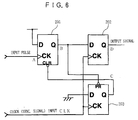
- Fig. 6 shows the synchronizing circuit for synchronizing the output signal of the MSGC.
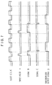
- Fig. 7 shows waveforms at various portions of the synchronizing circuit. These drawings show the circuit and waveforms for a single channel.
- an input pulse A from the MSGC 102 is input to the clock terminal of a first flip-flop 201, and an output pulse B from the Q terminal of the first flip-flop 201 is input to the D terminal of a second flip-flop 202. Further, an output pulse B from the Q terminal of the first flip-flop 201 is input to the PR (preset) terminal of a third flip-flop 203, and a clear signal from the CLR terminal of the first flip-flop 201 is input to the Q terminal of the third flip-flop 203.
- the clock (synchronization signal) input CLK are input to the CK terminals of the second and third flip-flops 202 and 203, respectively.
- the D terminal of the first flip-flop 201 is connected to a power supply line, and the D terminal of the third flip-flop 201 is connected to ground.
- An output signal; i.e., a signal synchronization output signal D, is output from the Q terminal of the second flip-flop 202.
- the CLR terminal of the first flip-flop 201 is connected to the Q terminal of the third flip-flop 203.
- the output signal B from the Q terminal of each of the first flip-flops 201 is connected to the PR terminal of the corresponding third flip-flop 203 via an OR circuit.
- the above-described circuit suffers the following problem.
- a signal is input at the same time as the synchronization clock, there arises a difficulty as to whether the input signal is to be regarded a signal in the previous period or a signal in the current period.
- the MSGC simultaneously outputs signals from a few adjacent signal lines; and if a time difference exists among these signals, these signals may be treated as two or more different events.
- the above-described circuit has wiring for avoiding such a problem.
- this portion does not have a significant meaning as a logic circuit, when timing is considered, the time difference corresponding to the delay (about 10 and a few nsec.) of the circuit can be absorbed. Since each period is separated from adjacent periods, an unavoidable dead time of about 10 nsec. exists in each period. However, parasitic event generation sterning from timing difference can be suppressed almost completely.
- the coordinate of an incident particle is to be obtained from the mean value thereof.
- the encoder circuit among the values assigned to signal lines that have output signals simultaneously in the same period, the highest and lowest values are selected, and the mean value of the highest and lowest values is calculated as a coordinate.
- Such calculation can be performed through use of an upper priority encoder and a lower priority encoder. That is, the value of an upper signal line and the value of a lower signal line are obtained through use of these encoders, and the average of these values is obtained.
- an encoder circuit that can receive a few hundreds of inputs is complicated and requires many elements, and the time required for the processing becomes long.
- the encoder circuit of the present MSGC there is employed a scheme that greatly simplifies the encoder circuit, taking into account that in the case of a valid input, signals are output from only a few adjacent signal lines.
- the input lines are divided into groups each including 16 signal lines.
- a logical sum of the output of the n th signal line of each group is obtained; and the logical sum is subjected to appropriate encoding in order to obtain the lower bits of the coordinate value.
- a logical sum of signals (8 signals) in each group is obtained and is then subjected to proper encoding in order to obtain the upper bits of the coordinate value.
- the operation for combining signals for the upper bit encoding and the lower bit encoding is performed through use of the same CPLDs as those used in the above-described signal synchronization circuit.
- Another CPLD is used for calculation of the final coordinate value and judgment as to where signals (duplicate signals) are output simultaneously from separated signal lines.
- Fig. 9 is a view schematically showing the structure of the data encoder of the present invention.
- the above-described synchronized output signal D is sent to a signal composite circuit 301, and an upper bit composite signal S U is connected to a duplication check circuit 302, an encoder 303, and a middle bit signal processing circuit 304.
- a lower bit composite signal S L is supplied to the middle bit signal processing circuit 304, an upper priority encoder 305, and a lower priority encoder 306.
- an output signal from the upper priority encoder 305 and an output signal from the lower priority encoder 306 are both sent to an adder 307 and to a subtracter 308.
- An output signal from the middle bit signal processing circuit 304 and an output signal from the subtracter 308 are input to the signal duplication check circuit 302.
- a duplication signal S D is fed from the signal duplication check circuit 302; an upper bit encode output is fed from the encoder 303; a middle bit encode output is fed from the middle bit signal processing circuit 304; a lower bit encoder output is fed from the adder 307; and a signal width output is fed from the subtracter 308.
- These signals are connected to a memory board via a J3 back plane bus of VME standard.
- a J3 back plane bus of VME standard For address signals for the X-axis and the y-axis, a common bus is used for every two data acquisition boards, while a hit signal is output independently from each board. Based on the hit signal, the source of an address signal presently output can be confirmed.
- the duplicate signals from the data acquisition boards are commonly output to a single bus.
- the functions of the storage device are to accumulate encoded signals from the respective data acquisition boards, and to serve as an interface with a computer on the VME bus.
- clocks of 20 MHz are generated and are supplied to the data acquisition boards as system clocks.
- the outputs from the data acquisition boards are in synchronicity with the clocks. Based on the hit signals and the duplication signals from the respective data acquisition bards, a judgment is made as to whether signals for each clock should be used as input signals.
- the signals are first input to a FIFO memory and are then stored in a DRAM having a capacity up to 512 MB.
- the content stored in the DRAM comprises an encoded hit position (position of an incident particle), a number of hit signal lines, a value of ADC externally input to the storage device, time at which the signals are recorded, and the like. These data are selectively used to form 32-bit data for each event. Therefore, the storage device temporarily stores data for 128 million events.
- the storage device has a VME bus interface, and is connected to the control computer via the bus.
- the computer can manipulate registers for controlling various operations of the storage device and can access to the DRAM in which the data are accumulated while using the same address space as that of the CPU. These structures enable the computer to easily handle the acquired data.
- Various kinds of computers can be used as the control computer provided that the computer conforms to the VME standard.
- a CPU-7V (product of FORCE Corp.) including microSPARC chips is used in combination with a UNIX operating system. Utilization of the strong network function of the UNIX operating system enables the data read out from the storage device by means of the computer to be transferred to a high-speed computer via a high-speed (100 BASE-T) local network, thereby enabling real-time analysis of a large amount of data.
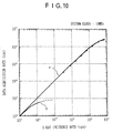
- Fig. 10 shows an actually measured correlation between X-ray incident intensity and actual data acquisition rate.
- Fig. 10 the horizontal axis represents X-ray incidence rate (cps), and the vertical axis represents data acquisition rate (cps).
- Curve a indicates the result obtained through use of the data acquisition system of the present invention, while curve b indicates the result obtained through use of a conventional data acquisition system.
- the frequency of clocks was set to 10 MHz.
- curve a when X-ray incidence rate exceeds 3 Mcps, the data acquisition rate saturates.
- the present data system has a linearity characteristic such that the data acquisition rate increases linearly up to 1 Mcps, and after 1 Mcps the linearity deteriorates gradually.
- the clock speed for data acquisition is 10 MHz, data cannot be acquired at this speed.
- the upper data acquisition speed is limited to 1/e according to Poisson statistics.
- Fig. 10 a data acquisition rate calculated on the basis of Poisson distribution is also shown.
- Figs. 11(a) and (b) show an example of a two-dimensional X-ray transmission image of a pendant obtained by use of the high speed data acquisition system of the present invention.
- Fig. 11(a) shows an image obtained through use of the conventional system in which a data acquisition rate corresponding to 5000 events is 6 x 10 2 cps.
- Fig. 11(b) shows an image obtained through use of the system of the present invention in which a data acquisition rate corresponding to 5 million events is 5.9 x 10 5 cps.
- a very clear X-ray image of a pendant can be obtained within a short period of time.
- combination of the MSGC and the high-speed data acquisition system enables high-speed processing of a large number of output signals from the imaging microstrip gas chamber, which in turn enables reliable measurement of particles.
- the MSGC combined with the high-speed data acquisition system of the present invention has sufficient potential as a real time X-ray area detector.
- X-ray crystallography is one of the fields where the MSGC is expected to be most useful. Since the MSGC has both good imaging capability and very fine timing resolution, the transition process of crystals can be measured with millisecond timing resolution.
- the MSGC according to the present invention enables a new analysis method for crystallography, called the "rotation continuous photograph (RCP)" method.
- a molecule is excited in the process of reactions.
- the excited structure has been observed by use of X-ray diffraction (XRD).
- XRD X-ray diffraction
- the lifetime of the excited state is very short (less than a few seconds), and only a few molecules in the sample are excited in the reaction. Therefore, until now observation of excited state by use of XRD has been impossible.
- the excited state has conventionally been observed only through a spectroscopic method or through some peculiar physical properties. The development of the real-time X-ray area detector would allow direct observation of the process of reactions.
- X-ray films or imaging plates have commonly been used for static XRD. Although an IP has good imaging capability and dynamic range, time resolved measurement is very difficult.
- the pulse counting detectors are usable for time resolved measurement. Proportional counters (PC), scintillation counters (SC), and solid semiconductor detectors (SSD) have conventionally been used. However, these conventional pulse counting detectors do not have sufficient imaging capability for real-time measurement, obtaining a two-dimensional diffraction pattern requires scanning on the plane or spherical surface.
- the MSGC of the present invention has both excellent imaging capability and a high timing resolution of 20 nsec., which allow high-speed timing analysis for direct observation of reaction processes.
- An example of observation of excited states is observation of light excitation of metal complexes, which will now be described.
- distortion of a diffraction pattern under light irradiation was observed for [Bu 4 N] 4 [Pt 2 (pop) 4 ] (pop denotes P 2 O 5 H 2 - ) through use of an X-ray powder diffractometer [Chem, Let, P. 829, 1997].
- One peak appearing in an X-ray powder pattern of [Bu 4 N] 4 [Pt 2 (pop) 4 ] was observed to move toward a higher diffraction angle when light was irradiated, and to return when the light was turned off.
- Figs. 12(a) and 12(b) show the structure of VO(acac) 2
- Figs. 13(a) and 13(b) show the structure of [Pt 2 (pop) 4
- Fig. 12(a) shows the three-dimensional structure of VO(acac) 2
- Fig. 12(b) shows the constitutional formula of VO(acac) 2
- Fig. 13(a) shows the three-dimensional structure of [Pt 2 (pop) 4 ]
- Fig. 13(b) shows the constitutional formula of [Pt 2 (pop) 4 ].
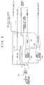
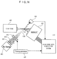
- Fig. 14 shows a schematic view of the experiment setup.
- numeral 102 denotes the MSGC according to the present invention
- numeral 110 denotes the high-speed data acquisition system according to the present invention
- numeral 401 denotes a xenon light source (xenon lamp);
- numeral 402 denotes a filter;
- numeral 403 denotes a convex lens;
- numeral 404 denotes a shutter,
- numeral 405 denotes an X-ray tube;
- numeral 406 denotes a photodiode;
- numeral 407 denotes a timing generator; and
- numeral 408 denotes a sample.
- the sample 408 was placed in front of the MSGC 102, and the distance between the sample 408 and the MSGC 102 was set to 8 - 9 cm.
- the xenon light was used as a light source for photo irradiation of the sample.
- the xenon light source 401 of 150W was placed at an angle of 45° with respect to the X-ray beam axis.
- the optical shutter 404 and the convex lens 403 were disposed between the xenon light source 401 and the sample 408.
- the filter 402 attached to the xenon light source 401 served to cut the infrared portion of xenon light.
- fluorescent X-rays from vanadium atoms in VO(acac) 2 was minimized through use of CrK ⁇ X-rays.
- the X-ray source was collimated to 1 mm ⁇ , and the tube voltage and current were set to 40 kV and 40 mA, respectively.
- the detector was slanted in the direction of the expected diffraction pattern (or point) so as to avoid the slant incident effect of the MSGC. In this experiment, the angle of this slant was 35 - 40°.
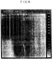
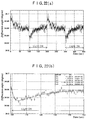
- Fig. 15 shows the image of Debye-Scherrer rings obtained by the MSGC.
- Fig. 15 vertical stripes represent discharge strips, while horizontal stripes are formed due to instability of the electronic readout apparatus. Since the detection plane of the MSGC is tilted away from the vertical plane of the incident X-ray beam, the shape of a Debye-Scherrer ring becomes an ellipse or a hyperbola.
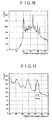
- Fig. 16 shows the powder diffraction pattern corresponding to a diffraction angle of 2 ⁇ for the same data as that of Fig. 15.
- the movement of the peak at 2 ⁇ 43° upon light irradiation was measured by the MSGC.
- the measured peak width was about 1°, which is due to the position resolution of the MSGC (200 ⁇ m bin width) and the size of the sample (0.5 mm ⁇ x 1 mm). Obtaining a precise diffraction angle requires a large amount of events and statistical analysis.
- the intensity of X-rays was 1.6 kW (40 kV, 40 mA), and the counting rate of the diffracted X-rays was about 10 4 cps.
- the counting rate in the peak of Fig. 17 was ⁇ 140 cps.
- the light irradiation was chopped every ten or two seconds by the optical shutter having an opening/closing time of 6 ms.
- the status of the light was monitored by a photodiode disposed behind the sample.
- the timing of the light chopping was tagged by the signal of the photodiode, and the timing for each X-ray event was recorded with the position data.
- Fig. 17 is the diffraction pattern near the proper peak.
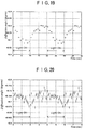
- the mean value and its error were calculated, and there were formed graphs shown in Figs. 19 and 20 in which the horizontal axis represents the elapsed time after light irradiation.
- Fig. 19 shows a first example of variation in diffraction angle due to on/off of light.
- one of the powder diffraction peaks of VO(acac) 2 was selected.
- the span of the data points is 1 sec.
- Fig. 20 shows a second example of variation in diffraction angle due to on/off of light.
- one of the powder diffraction peaks of VO(acac) 2 was selected.
- the span of the data points is 100 ms.
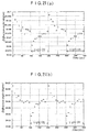
- Figs. 21(a) and 21(b) show variation in diffraction angle due to on/off of light, wherein Fig. 21(a) shows the measurement result for a diffraction angle of 35.7°, and Fig. 21(b) shows the measurement result for a diffraction angle of 34.7°.
- Figs. 22(a) and 22(b) show movement of the diffraction peak determined at 1-second intervals after the light is turned on.
- Fig. 23 shows the movement of the diffraction with variation in temperature.
- the crystal of [Bu 4 N] 4 [Pt 2 (pop) 4 ] has a tendency of thermal constriction. Therefore, it is concluded that the peak movement of the fast component is due to the light illumination, and the slow component is due to the thermal effect.
- a two-dimensional image of an X-ray diffraction pattern is not sufficient for obtaining the three-dimensional information of an objective crystal.
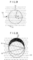
- Fig. 24 For any wavelength ⁇ of X-rays, the reflection points from the sample crystal appear on Ewald's sphere in the reciprocal lattice, as shown in Fig. 24.
- numeral 500 denotes an X-ray beam axis
- numeral 501 denotes Ewald's sphere
- numeral 502 denotes the reciprocal lattice.
- This reciprocal lattice space O must be located on Ewald's sphere, and the diametrical line including the origin corresponds to the path of the incident X-rays.
- the lattice is three dimensional, the conventional XRD method can provide only two-dimensional information. Then, another dimension is needed for obtaining the image of the reciprocal lattice.
- the Laue photograph is one of the popular techniques for obtaining the projection of the reciprocal lattice.
- a white X-ray beam By use of a white X-ray beam, the lattice point having a polar angle 2 ⁇ and an azimuth ⁇ is projected on an X-ray film.
- This method requires some known parameters, such as the crystal system, for reconstructing a three-dimensional point on the lattice for each spot. Therefore, for crystals of which axes are unknown, we must attempt to take several photographs so as to obtain an accurate axis.
- the diffraction angles of the points in the image are accumulated over the oscillated angles, and the exact structure of lattice has to be estimated through use of known parameters as well as the Laue photograph. Transforming the diffraction spots into the reciprocal lattice requires many trials involving various oscillation angles.
- the Weissenberg camera provides the other projection of the reciprocal lattice.
- the schematic structure of this camera is shown in Fig. 26.
- numeral 701 denotes a mechanism for rotating a cylindrical X-ray film
- numeral 702 denotes a screen
- numeral 703 denotes a cylindrical X-ray film
- numeral 704 denotes an X-ray beam
- numeral 705 denotes a sample crystal.
- the crystal 705 rotates about one of the crystal axes, and the cylindrical X-ray film 703 is moved simultaneously along the same axis of the rotation.
- a cylindrical slit is present between the sample crystal 705 and the X-ray film 703 in the direction of the axis of the rotation, and any one diffraction pattern layer (e.g., (hk0), (hk1) . . .) of the diffraction pattern is measured as a two-dimensional pattern along the rotation angle of the crystal. In this measurement, accurate coincidence of the rotation axis with one of the crystal axes is necessary. Mainly this method is used for obtaining the size and the crystal system of the unit cell.
- any one diffraction pattern layer e.g., (hk0), (hk1) . . .
- a four-axis X-ray diffractometer is generally employed.
- the sample crystal can be rotated about three axes ( ⁇ , ⁇ , ⁇ ), and the pulse counting detector (such as a scintillation counter or a proportional counter) is rotated about the 2 ⁇ axis.
- the pulse counting detector such as a scintillation counter or a proportional counter
- all the lattice points in reciprocal space within the sphere of 2/ ⁇ radius are measured exactly, as are the intensities of all spots. Since this detector is of a 0-dimensional (point-like) type, scanning all the reciprocal space takes much time. In general, 10 to 20 hours are required for measurement of a typical unorganized crystal.
- the MSGC can obtain both the positions and timings of incident X-rays. Since correspondence can be established between the rotational angle of the sample crystal and the timings of the incident X-rays, both the position of the diffraction spot and its rotational angle can be measured. Therefore, a wide region of the reciprocal space of the sample crystal is calculated simultaneously through use of only the data obtained by use of the MSGC.
- this method is called the Rotation Continuous Photograph (RCP) method. In this method, not only are the three-dimensional lattice points observed quickly (less than a few minutes depending on the light source intensity and the rotation speed), but also exact matching of the axis of crystal to the rotational axis is not required.
- An X-ray tube having a copper target and a nickel filter (K ⁇ : 8.0 keV) was used as an X-ray source.
- a single crystal of phenothiazine-benzilic acid complex was used.
- the sample was placed on the rotatable goniometer.
- the rotation speed of crystal was 216 seconds/cycle, which corresponds to 5/3 degree/second.
- the MSGG was placed normal to the X-ray beam, and the center of the beam was pointed at one edge of the detection area.
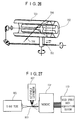
- Fig. 27 shows the schematic view for this experiment.
- numeral 801 denotes the X-ray tube (Cu target, 8.0 keV)
- numeral 802 denotes the rotatable goniometer (5/3 degree/second)
- numeral 803 denotes a sample.
- the positions of diffracted X-rays and their timings were measured by use of the MSGC 102 and the high-speed data acquisition system 110.
- the operating voltage and current of the X-ray tube were 40 kV and 40 mA, and the 1 mm ⁇ collimated X-ray beam was radiated to the sample 803.
- the size of sample 803 was about (0.5 mm) 3 . In this measurement, the counting rate was 2000 to 10000 events/second. All the time stamps for each X-ray event were recorded.
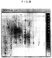
- Fig. 28 shows a two-dimensional image of diffraction pattern integrated during a single rotation of the crystal. In this drawing, many diffraction spots and much background X-ray noise can be seen. It is to be noted that the crystal axis is not precisely parallel to the rotation axis.
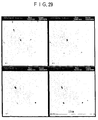
- Fig. 29 shows the time resolved sequential images observed every 0.3 second interval of exposure time. Each picture corresponds to 0.5° width of an oscillation X-ray picture. Diffraction points are found to be very clear as compared with the case of the integrated image shown in Fig. 28. In this measurement, the S/N ratio of diffraction spots in time (angle) resolved picture was 100 to 300.
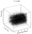
- Fig. 31 shows a three-dimensional image in which each spot is plotted according to its two-dimensional position (x, y) and the rotation angle of the crystal ( ⁇ ). The projection of this figure into the (y, ⁇ ) plane is shown in Fig. 31. Clear peaks concentrated over 0.5° can be found, indicating that the noise away from the peak can be easily removed through use of the angle information.
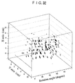
- Fig. 32 corresponds to Fig. 30 and shows the state in which the noise reduction method is employed.
Landscapes
- Physics & Mathematics (AREA)
- Health & Medical Sciences (AREA)
- Life Sciences & Earth Sciences (AREA)
- General Physics & Mathematics (AREA)
- High Energy & Nuclear Physics (AREA)
- Molecular Biology (AREA)
- Spectroscopy & Molecular Physics (AREA)
- Measurement Of Radiation (AREA)
- Electron Tubes For Measurement (AREA)
- Investigating Or Analysing Materials By Optical Means (AREA)
Abstract
Description
Claims (16)
- A microstrip gas chamber high-speed data acquisition system, characterized by comprising:(a) discrimination circuits for binary conversion of signals from anode strips and back strips of a two-dimensional microstrip gas chamber;(b) signal synchronizing circuits for converting binary asynchronous signals output from the discrimination circuits into clock-synchronized signals;(c) data encoder circuits connected to the signal synchronizing circuits;(d) an incident-particle hit judgment circuit connected to the data encoder circuits and operating such that when among a plurality of input signal lines for each of the vertical and horizontal axes a plurality of adjacent signal lines receive signals at the same timing, the incident-particle hit judgment circuit outputs a value corresponding to a signal line at the center of the adjacent signal lines, and when separated signal lines receive signals at the same timing, the incident-particle hit judgment circuit ignores the signals;(e) a storage device connected to the incident-particle hit judgment circuit and adapted to store, for each event, the vertical and horizontal coordinates of an incident particle, the timing of incidence of the particle, the degree of spreading of output signals, and the energy of the incident particle obtained from an overall pulse height; and(f) a computer connected to the storage device.
- A microstrip gas chamber high-speed data acquisition system according to Claim 1, characterized in that an amplifier is connected to each of the anode strips and back strips of the microstrip gas chamber, and an output signal from the amplifier is input to the corresponding discrimination circuit.
- A microstrip gas chamber high-speed data acquisition system according to Claim 1, characterized in that the data encoder circuit comprises an upper priory encoder, a lower priority encoder, and an adding circuit, and that the values of signals transmitted through upper and lower signal lines are obtained through use of the upper priory encoder and the lower priority encoder, and the mean value of the thus-obtained values is used for calculation of the coordinates of an incident particle.
- A microstrip gas chamber high-speed data acquisition system according to Claim 1, characterized in that each of the signal synchronizing circuits, the data encoder circuits, and the incident-particle hit judgment circuit is formed of a CPLD (Complex Programmable Logic Device).
- A microstrip gas chamber high-speed data acquisition system according to Claim 1, characterized in that the two-dimensional microstrip gas chamber comprises:(a) a substrate formed of organic thin film having elasticity;(b) anode strips and cathode strips formed on the substrate to be alternately arranged in parallel;(c) a high voltage source for applying high voltage between the anode strips and the cathode strips;(d) back strips formed on the lower face of the substrate to intersect the anode strips and the cathode strips;(e) a drift plate disposed a predetermined distance away from the substrate; and(f) a gas source for supplying a gas to be passed through a space between the surface of the substrate and the drift plate, wherein(g) electron amplification effect of the gas is caused, and signals regarding an X-ray or particle are extracted for simultaneous measurement of the two-dimensional coordinates of the X-ray or particle.
- A microstrip gas chamber high-speed data acquisition system according to Claim 5, characterized in that the opposite edge portions of each of the cathode strips are coated with organic thin film having elasticity.
- A microstrip gas chamber high-speed data acquisition system according to Claim 5 or 6, characterized in that the organic thin film having elasticity is polyimide film.
- A microstrip gas chamber high-speed data acquisition system according to Claim 5, characterized in that the surface of the substrate is coated with organic titanium in order to control the surface resistance.
- A microstrip gas chamber high-speed data acquisition system according to Claim 5, characterized in that an IC package is provided under the back strips, and the IC package is an LSI high-density package.
- A microstrip gas chamber high-speed data acquisition system according to Claim 5, characterized in that the back strips are connected to first bonding pads on the top surface of the substrate through fine through-holes; the edge portion of the IC package is raised to form a wall portion; second bonding pads are formed on the top surface of the wall portion; and the first and second bonding pads are connected with each other through use of bonding wires.
- A microstrip gas chamber high-speed data acquisition system according to Claim 5, characterized in that the two-dimensional microstrip gas chamber is used as an X-ray imaging detector by use of X-ray irradiation.
- A method of measuring a sample, characterized by comprising the step of constructing a microstrip gas chamber high-speed data acquisition system including:discrimination circuits for binary conversion of signals from anode strips and back strips of a two-dimensional microstrip gas chamber;signal synchronizing circuits for converting binary asynchronous signals output from the discrimination circuits into clock-synchronized signals;data encoder circuits connected to the signal synchronizing circuits;an incident-particle hit judgment circuit connected to the data encoder circuits and operating such that when among a plurality of input signal lines for each of the vertical and horizontal axes a plurality of adjacent signal lines receive signals at the same timing, the incident-particle hit judgment circuit outputs a value corresponding to a signal line at the center of the adjacent signal lines, and when separated signal lines receive signals at the same timing, the incident-particle hit judgment circuit ignores the signals;a storage device connected to the incident-particle hit judgment circuit and adapted to store, for each event, the vertical and horizontal coordinates of an incident particle, the timing of incidence of the particle, the degree of spreading of output signals, and the energy of the incident particle obtained from an overall pulse height; anda computer connected to the storage device, wherein the two-dimensional microstrip gas chamber includes:a substrate formed of organic thin film having elasticity;anode strips and cathode strips formed on the substrate to be alternately arranged in parallel;a high voltage source for applying high voltage between the anode strips and the cathode strips;back strips formed on the lower face of the substrate to intersect the anode strips and the cathode strips;a drift plane disposed a predetermined distance away from the substrate; anda gas source for supplying a gas to be passed through a space between the surface of the substrate and the drift plane, whereinan X-ray beam is radiated onto a moving sample, and the process of fast changes of the sample is directly observing by X-ray diffraction.
- A method of measuring a sample according to Claim 12, characterized in that the sample is a solid crystal, and the process of changes in the structure of the solid crystal is directly observed.
- A method of measuring a sample according to Claim 12, characterized in that the process of change in the sample is measured at intervals of 1/1000 second or less.
- A method of measuring a sample according to Claim 13, characterized in that an excited state of the solid crystal is observed.
- A method of measuring a sample according to Claim 12, characterized in that measurement is performed in accordance with a rotation continuous photograph method; and the position of an X-ray resulting from X-ray diffraction during the measurement and the timing of the X-ray diffraction are measured so as to determine a three-dimensional crystalline structure.
Applications Claiming Priority (6)
| Application Number | Priority Date | Filing Date | Title |
|---|---|---|---|
| JP171389/97 | 1997-06-27 | ||
| JP17138997 | 1997-06-27 | ||
| JP17138997 | 1997-06-27 | ||
| JP10089750A JP2843319B1 (en) | 1997-06-27 | 1998-04-02 | Microstrip gas chamber high-speed data acquisition system and sample measurement method using the same |
| JP89750/98 | 1998-04-02 | ||
| JP8975098 | 1998-04-02 |
Publications (3)
| Publication Number | Publication Date |
|---|---|
| EP0887752A2 true EP0887752A2 (en) | 1998-12-30 |
| EP0887752A3 EP0887752A3 (en) | 2005-12-21 |
| EP0887752B1 EP0887752B1 (en) | 2008-04-16 |
Family
ID=26431154
Family Applications (1)
| Application Number | Title | Priority Date | Filing Date |
|---|---|---|---|
| EP98110642A Expired - Lifetime EP0887752B1 (en) | 1997-06-27 | 1998-06-10 | Microstrip gas chamber high-speed data acquisition system and method of measuring samples by use of the system |
Country Status (4)
| Country | Link |
|---|---|
| US (2) | US6097032A (en) |
| EP (1) | EP0887752B1 (en) |
| JP (1) | JP2843319B1 (en) |
| DE (1) | DE69839362T2 (en) |
Cited By (3)
| Publication number | Priority date | Publication date | Assignee | Title |
|---|---|---|---|---|
| WO2002001598A1 (en) * | 2000-06-27 | 2002-01-03 | Hiroyuki Takahashi | Microstrip gas chamber |
| EP1891464A4 (en) * | 2005-06-16 | 2013-02-13 | Integrated Sensors Llc | Plasma panel based ionizing-photon radiation detector |
| US8835863B2 (en) | 2012-03-07 | 2014-09-16 | Panasonic Corporation | Radiation detector |
Families Citing this family (52)
| Publication number | Priority date | Publication date | Assignee | Title |
|---|---|---|---|---|
| WO1997029507A1 (en) * | 1996-02-12 | 1997-08-14 | University Of Akron, The | Multimedia detectors for medical imaging |
| US6703619B2 (en) | 2000-02-02 | 2004-03-09 | Hiroyuki Takahashi | Multi-grid type microstrip gas chamber |
| US7901939B2 (en) | 2002-05-09 | 2011-03-08 | University Of Chicago | Method for performing crystallization and reactions in pressure-driven fluid plugs |
| DE60333995D1 (en) | 2002-05-09 | 2010-10-14 | Univ Chicago | DEVICE AND METHOD FOR PRESSURE-CONTROLLED PLUG TRANSPORT AND REACTION |
| US8198812B1 (en) | 2002-05-21 | 2012-06-12 | Imaging Systems Technology | Gas filled detector shell with dipole antenna |
| US20100022414A1 (en) | 2008-07-18 | 2010-01-28 | Raindance Technologies, Inc. | Droplet Libraries |
| GB0307428D0 (en) | 2003-03-31 | 2003-05-07 | Medical Res Council | Compartmentalised combinatorial chemistry |
| US20060078893A1 (en) | 2004-10-12 | 2006-04-13 | Medical Research Council | Compartmentalised combinatorial chemistry by microfluidic control |
| GB0307403D0 (en) | 2003-03-31 | 2003-05-07 | Medical Res Council | Selection by compartmentalised screening |
| IL159824A (en) * | 2004-01-12 | 2012-05-31 | Xurity Ltd | Xrd means for identifying materials in a volume of interest and a method therefor |
| US20050221339A1 (en) | 2004-03-31 | 2005-10-06 | Medical Research Council Harvard University | Compartmentalised screening by microfluidic control |
| US7564039B1 (en) * | 2004-06-17 | 2009-07-21 | Integrated Sensors, Llc | Dual substrate plasma panel based ionizing radiation detector |
| US7332726B2 (en) * | 2004-06-19 | 2008-02-19 | Integrated Sensors, Llc | Plasma panel based ionizing radiation detector |
| US7968287B2 (en) | 2004-10-08 | 2011-06-28 | Medical Research Council Harvard University | In vitro evolution in microfluidic systems |
| WO2007025221A2 (en) * | 2005-08-24 | 2007-03-01 | The Scripps Research Institute | Protein structure determination |
| EP1984738A2 (en) | 2006-01-11 | 2008-10-29 | Raindance Technologies, Inc. | Microfluidic devices and methods of use in the formation and control of nanoreactors |
| US9562837B2 (en) | 2006-05-11 | 2017-02-07 | Raindance Technologies, Inc. | Systems for handling microfludic droplets |
| EP4190448A3 (en) | 2006-05-11 | 2023-09-20 | Bio-Rad Laboratories, Inc. | Microfluidic devices |
| US9012390B2 (en) | 2006-08-07 | 2015-04-21 | Raindance Technologies, Inc. | Fluorocarbon emulsion stabilizing surfactants |
| WO2008133710A2 (en) | 2006-10-28 | 2008-11-06 | Integrated Sensors, Llc | Plasma panel based radiation detector |
| US8772046B2 (en) | 2007-02-06 | 2014-07-08 | Brandeis University | Manipulation of fluids and reactions in microfluidic systems |
| US8592221B2 (en) | 2007-04-19 | 2013-11-26 | Brandeis University | Manipulation of fluids, fluid components and reactions in microfluidic systems |
| US12038438B2 (en) | 2008-07-18 | 2024-07-16 | Bio-Rad Laboratories, Inc. | Enzyme quantification |
| US8528589B2 (en) | 2009-03-23 | 2013-09-10 | Raindance Technologies, Inc. | Manipulation of microfluidic droplets |
| EP2422218A4 (en) * | 2009-04-20 | 2013-12-18 | Integrated Sensors Llp | DETECTOR FOR IONIZING PARTICLE RADIATION ON PLASMATE ROBUST |
| EP2486409A1 (en) | 2009-10-09 | 2012-08-15 | Universite De Strasbourg | Labelled silica-based nanomaterial with enhanced properties and uses thereof |
| EP2517025B1 (en) | 2009-12-23 | 2019-11-27 | Bio-Rad Laboratories, Inc. | Methods for reducing the exchange of molecules between droplets |
| EP4435111A1 (en) | 2010-02-12 | 2024-09-25 | Bio-Rad Laboratories, Inc. | Digital analyte analysis |
| US9399797B2 (en) | 2010-02-12 | 2016-07-26 | Raindance Technologies, Inc. | Digital analyte analysis |
| US9366632B2 (en) | 2010-02-12 | 2016-06-14 | Raindance Technologies, Inc. | Digital analyte analysis |
| US10351905B2 (en) | 2010-02-12 | 2019-07-16 | Bio-Rad Laboratories, Inc. | Digital analyte analysis |
| JP5427655B2 (en) * | 2010-03-11 | 2014-02-26 | 株式会社日立製作所 | Radiation measurement equipment, nuclear medicine diagnostic equipment |
| WO2012045012A2 (en) | 2010-09-30 | 2012-04-05 | Raindance Technologies, Inc. | Sandwich assays in droplets |
| JP2012168170A (en) * | 2011-01-25 | 2012-09-06 | Dainippon Printing Co Ltd | Radiation detector using gas amplification |
| US9364803B2 (en) | 2011-02-11 | 2016-06-14 | Raindance Technologies, Inc. | Methods for forming mixed droplets |
| EP2675819B1 (en) | 2011-02-18 | 2020-04-08 | Bio-Rad Laboratories, Inc. | Compositions and methods for molecular labeling |
| US8841071B2 (en) | 2011-06-02 | 2014-09-23 | Raindance Technologies, Inc. | Sample multiplexing |
| WO2012167142A2 (en) | 2011-06-02 | 2012-12-06 | Raindance Technolgies, Inc. | Enzyme quantification |
| US8658430B2 (en) | 2011-07-20 | 2014-02-25 | Raindance Technologies, Inc. | Manipulating droplet size |
| JP2015099015A (en) * | 2012-03-07 | 2015-05-28 | パナソニック株式会社 | Radiation detector |
| JP2015099013A (en) * | 2012-03-07 | 2015-05-28 | パナソニック株式会社 | Radiation detector |
| JP2015099014A (en) * | 2012-03-07 | 2015-05-28 | パナソニック株式会社 | Radiation detector |
| US9529099B2 (en) | 2012-11-14 | 2016-12-27 | Integrated Sensors, Llc | Microcavity plasma panel radiation detector |
| US9964651B2 (en) | 2013-03-15 | 2018-05-08 | Integrated Sensors, Llc | Ultra-thin plasma panel radiation detector |
| US9551795B2 (en) | 2013-03-15 | 2017-01-24 | Integrated Sensors, Llc | Ultra-thin plasma radiation detector |
| US11901041B2 (en) | 2013-10-04 | 2024-02-13 | Bio-Rad Laboratories, Inc. | Digital analysis of nucleic acid modification |
| US9944977B2 (en) | 2013-12-12 | 2018-04-17 | Raindance Technologies, Inc. | Distinguishing rare variations in a nucleic acid sequence from a sample |
| WO2015103367A1 (en) | 2013-12-31 | 2015-07-09 | Raindance Technologies, Inc. | System and method for detection of rna species |
| US10647981B1 (en) | 2015-09-08 | 2020-05-12 | Bio-Rad Laboratories, Inc. | Nucleic acid library generation methods and compositions |
| US11035804B2 (en) | 2017-06-28 | 2021-06-15 | Kla Corporation | System and method for x-ray imaging and classification of volume defects |
| CN111678934B (en) * | 2020-06-10 | 2023-05-09 | 首钢集团有限公司 | The method of testing the P ratio of the phosphating film on the continuous annealing plate by the XRD method of the Cr target |
| WO2023141773A1 (en) * | 2022-01-25 | 2023-08-03 | 京东方科技集团股份有限公司 | Detection substrate and ray detector |
Family Cites Families (4)
| Publication number | Priority date | Publication date | Assignee | Title |
|---|---|---|---|---|
| US4379967A (en) * | 1980-08-22 | 1983-04-12 | Mcintyre John A | Fiber optic matrix coding method and apparatus for radiation image amplifier |
| US4642466A (en) * | 1985-03-05 | 1987-02-10 | The United States Of America As Represented By The United States Department Of Energy | Fast counting electronics for neutron coincidence counting |
| JP3418402B2 (en) * | 1993-10-20 | 2003-06-23 | ケンブリッジ・イメージング・リミテッド | Improved imaging method and apparatus |
| US5500534A (en) * | 1994-03-31 | 1996-03-19 | Iowa State University Research Foundation | Integrated energy-sensitive and position-sensitive x-ray detection system |
-
1998
- 1998-04-02 JP JP10089750A patent/JP2843319B1/en not_active Expired - Fee Related
- 1998-06-03 US US09/089,882 patent/US6097032A/en not_active Expired - Lifetime
- 1998-06-10 DE DE69839362T patent/DE69839362T2/en not_active Expired - Lifetime
- 1998-06-10 EP EP98110642A patent/EP0887752B1/en not_active Expired - Lifetime
-
1999
- 1999-11-12 US US09/441,157 patent/US6118849A/en not_active Expired - Fee Related
Cited By (4)
| Publication number | Priority date | Publication date | Assignee | Title |
|---|---|---|---|---|
| WO2002001598A1 (en) * | 2000-06-27 | 2002-01-03 | Hiroyuki Takahashi | Microstrip gas chamber |
| US6933506B2 (en) | 2000-06-27 | 2005-08-23 | Hiroyuki Takahashi | Microstrip gas chamber |
| EP1891464A4 (en) * | 2005-06-16 | 2013-02-13 | Integrated Sensors Llc | Plasma panel based ionizing-photon radiation detector |
| US8835863B2 (en) | 2012-03-07 | 2014-09-16 | Panasonic Corporation | Radiation detector |
Also Published As
| Publication number | Publication date |
|---|---|
| JP2843319B1 (en) | 1999-01-06 |
| EP0887752B1 (en) | 2008-04-16 |
| JPH1172569A (en) | 1999-03-16 |
| DE69839362D1 (en) | 2008-05-29 |
| US6097032A (en) | 2000-08-01 |
| US6118849A (en) | 2000-09-12 |
| DE69839362T2 (en) | 2008-07-24 |
| EP0887752A3 (en) | 2005-12-21 |
Similar Documents
| Publication | Publication Date | Title |
|---|---|---|
| US6097032A (en) | Microstrip gas chamber high-speed data acquisition system and method of measuring samples by use of the system | |
| Broennimann et al. | The PILATUS 1M detector | |
| EP1739413B1 (en) | X-ray diffraction apparatus | |
| EP2208089B1 (en) | Detector for hard x-radiation | |
| US20060208196A1 (en) | Method and apparatus for gamma ray detection | |
| JPH05505025A (en) | X-ray imaging system and its solid state detector | |
| JP2000504832A (en) | Multimedia detector for medical images | |
| JP2002514772A (en) | Multi-purpose multi-density multi-atomic number detector media | |
| Pooley et al. | Development of the “GP2” detector: modification of the PImMS CMOS sensor for energy-resolved neutron radiography | |
| JP3535045B2 (en) | Device for determining gamma-ray incident direction from trajectory image of recoil electrons by MSGC | |
| Polichar et al. | Development of CdZnTe energy selective arrays for industrial and medical radiation imaging | |
| CN111380884A (en) | Single-source energy resolution type X-ray diffraction analysis and tomography coupling device | |
| US20040120459A1 (en) | Industrial machine vision system having a direct conversion X-ray detector | |
| Tanimori et al. | Development of a MicroStrip Gas Chamber as a Time-Resolved Area Detector | |
| Arfelli et al. | Digital mammography at the Trieste synchrotron light source | |
| Helliwell et al. | A 2D MWPC area detector for use with synchrotron X-radiation at the Daresbury laboratory for small angle diffraction and scattering | |
| Iwanczyk et al. | The HgI2 array detector development project | |
| Ochi et al. | Development of an ultra-fast data-acquisition system for a two-dimensional microstrip gas chamber | |
| De Lurgio et al. | A neutron detector to monitor the intensity of transmitted neutrons for small-angle neutron scattering instruments | |
| Ochi et al. | Development of imaging microstrip gas chambers and measurement of the polarization of X-rays | |
| Bertolucci et al. | Portable system for imaging of/spl alpha/, and X-ray sources with silicon pixel detectors and Medipix1 readout | |
| JP2005121528A (en) | Two-dimensional image element, two-dimensional image detecting device and x-ray-analysis device using the same | |
| Jernigan et al. | Performance measurements of hybrid PIN diode arrays | |
| Uno et al. | Development of neutron gaseous detector with GEM | |
| Milch | X-ray detectors for diffraction studies and their use with synchrotron radiation |
Legal Events
| Date | Code | Title | Description |
|---|---|---|---|
| PUAI | Public reference made under article 153(3) epc to a published international application that has entered the european phase |
Free format text: ORIGINAL CODE: 0009012 |
|
| AK | Designated contracting states |
Kind code of ref document: A2 Designated state(s): AT BE CH CY DE DK ES FI FR GB GR IE IT LI LU MC NL PT SE |
|
| AX | Request for extension of the european patent |
Free format text: AL;LT;LV;MK;RO;SI |
|
| RAP1 | Party data changed (applicant data changed or rights of an application transferred) |
Owner name: JAPAN SCIENCE AND TECHNOLOGY AGENCY |
|
| RAP1 | Party data changed (applicant data changed or rights of an application transferred) |
Owner name: JAPAN SCIENCE AND TECHNOLOGY AGENCY |
|
| PUAL | Search report despatched |
Free format text: ORIGINAL CODE: 0009013 |
|
| AK | Designated contracting states |
Kind code of ref document: A3 Designated state(s): AT BE CH CY DE DK ES FI FR GB GR IE IT LI LU MC NL PT SE |
|
| AX | Request for extension of the european patent |
Extension state: AL LT LV MK RO SI |
|
| RIC1 | Information provided on ipc code assigned before grant |
Ipc: 7G 01T 1/29 B Ipc: 7G 01T 1/17 B Ipc: 7G 06F 17/40 A |
|
| 17P | Request for examination filed |
Effective date: 20060210 |
|
| 17Q | First examination report despatched |
Effective date: 20060717 |
|
| AKX | Designation fees paid |
Designated state(s): DE FR GB NL |
|
| GRAP | Despatch of communication of intention to grant a patent |
Free format text: ORIGINAL CODE: EPIDOSNIGR1 |
|
| GRAS | Grant fee paid |
Free format text: ORIGINAL CODE: EPIDOSNIGR3 |
|
| GRAA | (expected) grant |
Free format text: ORIGINAL CODE: 0009210 |
|
| AK | Designated contracting states |
Kind code of ref document: B1 Designated state(s): DE FR GB NL |
|
| REF | Corresponds to: |
Ref document number: 69839362 Country of ref document: DE Date of ref document: 20080529 Kind code of ref document: P |
|
| ET | Fr: translation filed | ||
| PLBE | No opposition filed within time limit |
Free format text: ORIGINAL CODE: 0009261 |
|
| STAA | Information on the status of an ep patent application or granted ep patent |
Free format text: STATUS: NO OPPOSITION FILED WITHIN TIME LIMIT |
|
| 26N | No opposition filed |
Effective date: 20090119 |
|
| PGFP | Annual fee paid to national office [announced via postgrant information from national office to epo] |
Ref country code: DE Payment date: 20120622 Year of fee payment: 15 Ref country code: NL Payment date: 20120626 Year of fee payment: 15 |
|
| PGFP | Annual fee paid to national office [announced via postgrant information from national office to epo] |
Ref country code: GB Payment date: 20120622 Year of fee payment: 15 Ref country code: FR Payment date: 20120705 Year of fee payment: 15 |
|
| REG | Reference to a national code |
Ref country code: NL Ref legal event code: V1 Effective date: 20140101 |
|
| GBPC | Gb: european patent ceased through non-payment of renewal fee |
Effective date: 20130610 |
|
| REG | Reference to a national code |
Ref country code: DE Ref legal event code: R119 Ref document number: 69839362 Country of ref document: DE Effective date: 20140101 |
|
| REG | Reference to a national code |
Ref country code: FR Ref legal event code: ST Effective date: 20140228 |
|
| PG25 | Lapsed in a contracting state [announced via postgrant information from national office to epo] |
Ref country code: DE Free format text: LAPSE BECAUSE OF NON-PAYMENT OF DUE FEES Effective date: 20140101 Ref country code: NL Free format text: LAPSE BECAUSE OF NON-PAYMENT OF DUE FEES Effective date: 20140101 Ref country code: GB Free format text: LAPSE BECAUSE OF NON-PAYMENT OF DUE FEES Effective date: 20130610 |
|
| PG25 | Lapsed in a contracting state [announced via postgrant information from national office to epo] |
Ref country code: FR Free format text: LAPSE BECAUSE OF NON-PAYMENT OF DUE FEES Effective date: 20130701 |