EP0887689B1 - System zur optischen Zeilenverschiebung für eine fehlertolerante Projektionsanzeigevorrichtung - Google Patents
System zur optischen Zeilenverschiebung für eine fehlertolerante Projektionsanzeigevorrichtung Download PDFInfo
- Publication number
- EP0887689B1 EP0887689B1 EP98303737.5A EP98303737A EP0887689B1 EP 0887689 B1 EP0887689 B1 EP 0887689B1 EP 98303737 A EP98303737 A EP 98303737A EP 0887689 B1 EP0887689 B1 EP 0887689B1
- Authority
- EP
- European Patent Office
- Prior art keywords
- light
- row
- pixel
- image
- array
- Prior art date
- Legal status (The legal status is an assumption and is not a legal conclusion. Google has not performed a legal analysis and makes no representation as to the accuracy of the status listed.)
- Expired - Lifetime
Links
- 238000006073 displacement reaction Methods 0.000 title claims description 32
- 230000003287 optical effect Effects 0.000 title claims description 18
- 230000000007 visual effect Effects 0.000 claims description 12
- 230000000737 periodic effect Effects 0.000 claims description 4
- 230000033001 locomotion Effects 0.000 description 33
- 230000003534 oscillatory effect Effects 0.000 description 17
- 238000003491 array Methods 0.000 description 16
- 230000002950 deficient Effects 0.000 description 13
- 230000007246 mechanism Effects 0.000 description 11
- 238000000034 method Methods 0.000 description 11
- 238000012937 correction Methods 0.000 description 10
- 239000000758 substrate Substances 0.000 description 10
- 230000005540 biological transmission Effects 0.000 description 8
- 230000007547 defect Effects 0.000 description 7
- 238000012545 processing Methods 0.000 description 7
- 230000004044 response Effects 0.000 description 7
- 239000006096 absorbing agent Substances 0.000 description 6
- 238000004519 manufacturing process Methods 0.000 description 4
- 230000010355 oscillation Effects 0.000 description 3
- 238000005282 brightening Methods 0.000 description 2
- 230000008859 change Effects 0.000 description 2
- 230000003247 decreasing effect Effects 0.000 description 2
- 239000012530 fluid Substances 0.000 description 2
- 238000007689 inspection Methods 0.000 description 2
- 239000004973 liquid crystal related substance Substances 0.000 description 2
- 238000013519 translation Methods 0.000 description 2
- 238000012935 Averaging Methods 0.000 description 1
- 239000004988 Nematic liquid crystal Substances 0.000 description 1
- 238000010521 absorption reaction Methods 0.000 description 1
- 230000001133 acceleration Effects 0.000 description 1
- 238000013459 approach Methods 0.000 description 1
- 230000000903 blocking effect Effects 0.000 description 1
- 230000000052 comparative effect Effects 0.000 description 1
- 230000003467 diminishing effect Effects 0.000 description 1
- 238000009826 distribution Methods 0.000 description 1
- 230000000694 effects Effects 0.000 description 1
- 230000006870 function Effects 0.000 description 1
- 230000004927 fusion Effects 0.000 description 1
- 238000009499 grossing Methods 0.000 description 1
- 239000011159 matrix material Substances 0.000 description 1
- 238000012986 modification Methods 0.000 description 1
- 230000004048 modification Effects 0.000 description 1
- 238000002310 reflectometry Methods 0.000 description 1
- 230000000246 remedial effect Effects 0.000 description 1
- 229910052710 silicon Inorganic materials 0.000 description 1
- 230000002123 temporal effect Effects 0.000 description 1
- 230000016776 visual perception Effects 0.000 description 1
Images


Classifications
-
- G—PHYSICS
- G09—EDUCATION; CRYPTOGRAPHY; DISPLAY; ADVERTISING; SEALS
- G09G—ARRANGEMENTS OR CIRCUITS FOR CONTROL OF INDICATING DEVICES USING STATIC MEANS TO PRESENT VARIABLE INFORMATION
- G09G3/00—Control arrangements or circuits, of interest only in connection with visual indicators other than cathode-ray tubes
- G09G3/007—Use of pixel shift techniques, e.g. by mechanical shift of the physical pixels or by optical shift of the perceived pixels
-
- H—ELECTRICITY
- H04—ELECTRIC COMMUNICATION TECHNIQUE
- H04N—PICTORIAL COMMUNICATION, e.g. TELEVISION
- H04N9/00—Details of colour television systems
- H04N9/12—Picture reproducers
- H04N9/31—Projection devices for colour picture display, e.g. using electronic spatial light modulators [ESLM]
- H04N9/3102—Projection devices for colour picture display, e.g. using electronic spatial light modulators [ESLM] using two-dimensional electronic spatial light modulators
- H04N9/312—Driving therefor
-
- H—ELECTRICITY
- H04—ELECTRIC COMMUNICATION TECHNIQUE
- H04N—PICTORIAL COMMUNICATION, e.g. TELEVISION
- H04N9/00—Details of colour television systems
- H04N9/12—Picture reproducers
- H04N9/31—Projection devices for colour picture display, e.g. using electronic spatial light modulators [ESLM]
- H04N9/3179—Video signal processing therefor
- H04N9/3182—Colour adjustment, e.g. white balance, shading or gamut
-
- G—PHYSICS
- G09—EDUCATION; CRYPTOGRAPHY; DISPLAY; ADVERTISING; SEALS
- G09G—ARRANGEMENTS OR CIRCUITS FOR CONTROL OF INDICATING DEVICES USING STATIC MEANS TO PRESENT VARIABLE INFORMATION
- G09G2330/00—Aspects of power supply; Aspects of display protection and defect management
- G09G2330/08—Fault-tolerant or redundant circuits, or circuits in which repair of defects is prepared
-
- G—PHYSICS
- G09—EDUCATION; CRYPTOGRAPHY; DISPLAY; ADVERTISING; SEALS
- G09G—ARRANGEMENTS OR CIRCUITS FOR CONTROL OF INDICATING DEVICES USING STATIC MEANS TO PRESENT VARIABLE INFORMATION
- G09G3/00—Control arrangements or circuits, of interest only in connection with visual indicators other than cathode-ray tubes
- G09G3/001—Control arrangements or circuits, of interest only in connection with visual indicators other than cathode-ray tubes using specific devices not provided for in groups G09G3/02 - G09G3/36, e.g. using an intermediate record carrier such as a film slide; Projection systems; Display of non-alphanumerical information, solely or in combination with alphanumerical information, e.g. digital display on projected diapositive as background
Definitions
- the present invention relates to two dimensional display systems. More particularly, the present invention relates to fault correction for non-working or damaged pixels of such light modulator arrays by optically displacing selected rows of light modulators.
- High resolution display systems based on discrete two dimensional arrays of reflective or transmissive elements (visually recognized as "pixels") are used in portable computers, LCD multimedia projectors, high definition televisions, flat panel displays, and virtual reality eyewear.
- pixels discrete two dimensional arrays of reflective or transmissive elements
- LCD multimedia projectors high definition televisions
- flat panel displays flat panel displays
- virtual reality eyewear As compared to conventional scanning or projection devices (e.g. cathode ray tubes or video projectors), such devices operate at low voltages, making them power efficient, and generally do not require long optical paths for operation, making them space efficient.
- a typical two dimensional array (using, for example, LCD's that control light transmission or micro-mirrors that control light reflection) may have a million or more discrete elements, with failure of only two or three elements making the display system useless. Even worse, initially operable two dimensional arrays may degrade in performance due to pinpoint screen damage, electronic failures, or mechanical wear and stiction problems. Particularly worrisome are display driver or mounting defects that can cause entire rows or columns of elements in the two dimensional array to simultaneously fail.
- US-A-5 504 504 discloses a method and display system for reducing the visual impact of defects present in an image display comprising an array of pixels.
- Each non-defective pixel is selectively operable in response to input data by addressing facilities between an "on" state, in which light is directed onto a viewing surface, and an "off" state, in which light is not directed onto the viewing surface.
- Each defective pixel is immediately surrounded by a first ring of compensation pixels adjacent to the central defective pixel.
- the compensation pixels are immediately surrounded by a second ring of reference pixels spaced from the central defective pixel.
- the addressing circuit-determined value of at least one compensation pixel in the first ring surrounding the defective pixel is changed to a corrective value, in order to reduce the visual impact of the defect.
- fault tolerance should allow for failure of single display elements, multiple display elements, or even failure of multiple rows or columns of display elements without appreciably diminishing display quality.
- fault correction in such a fault tolerant system can be accomplished dynamically, and failure of array elements may even be corrected in real time.
- a visual display system comprising: a light source, a visible display surface, a two dimensional light modulator array having a plurality of light modulators arranged in a first row and a second row to modulate light from the light source, with light modulated by the first row presented as a first row of pixels on the display surface, and light modulated by the second row presented as a second row of pixels on the display surface, and at least one optical element adapted, in a first state, to direct light modulated by the first and second rows, respectively, to first and second rows on the display surface; and, in a second state, to direct the light modulated by the first row to the second row on the display surface; the at least one optical element adapted to periodically switch between a first and a second state so as to compensate for a failure in at least one of the second row of light modulators.
- Two dimensional row and column displacement by various mechanical or optical mechanisms is within the scope of the present invention.
- light modulators arranged in a first column and a second column can be positioned substantially orthogonal to the first row and second row, with the first column at a first column position with respect to the fixed substrate and the second column at a second column position with respect to the fixed substrate.
- the movable element can then displace (mechanically or optically) the first column from its first column position to substantially occupy the second column position, as well as providing for row displacement for two dimensional movement.
- the same virtual pixel can result from the periodic display of four physical pixels that are sequentially moved into position by displacement of the physical pixel array one pixel leftward, one row upward, one column rightward, and one row downward back to the original position.
- microelectromechanical pivoting or deformable mirrors controllably movable in response to applied electrostatic or electromagnetic forces are preferred for reflective displays.
- Such mirror systems are commercially available from Texas Instruments as part of a Digital Mirror Device (DMD) colour projection system.
- DMD Digital Mirror Device
- switchable diffractive light valves such as developed by Silicon Light Machines, Sunnyvale, CA may be used.
- displays based on ferroelectric, electroluminescent, or twisted nematic liquid crystals can also be used. Also suitable are displays that can directly switch to an appropriate transmissive gray level without requiring use of time resolved gray levels such as needed for bistable reflective devices.
- any device capable of modifying gray levels with a frequency exceeding about 10HZ, or more typically, with a frequency between about 100HZ and 1000Hz, whether directly in response to variable analog current such as with liquid crystals, or through time based techniques such as employed by digital micromirrors or diffractive light valves, can be used in the present invention.
- Figure 1 is a schematic, partially broken away view of a fault tolerant display system 10 (which does not form part of the invention) capable of supporting mechanisms for mechanically or optically compensating for failed, defective, or intermittently operating pixels in a display.
- Figure 1 illustrates both a transmissive display system 20 and a reflective display 40 supported by a movable element 14 on a common fixed substrate 12.
- the transmissive display system 20 includes a row and column array 24 of light transmissive display elements 28 to selectively transmit or absorb light from a light source 22, while the reflective display system 40 includes a row and column array 42 of pivotal mirrors 44 that selectively alter reflective direction of light from light source 50.
- a given display will usually contain either transmissive elements (such as a conventional active matrix LCD projector, LCD display, or ferroelectric fluid display) or reflective elements (such as a digital micromirror disclosed, for example, in U.S. Patent 5,535,047 to Hornbeck ), although certain embodiments may combine transmissive and reflective elements for operation (e.g. a stacked transmissive/reflective display using LCD's and a selectively deformable sheet mirror as discussed later in connection with Figure 10 ).
- transmissive elements such as a conventional active matrix LCD projector, LCD display, or ferroelectric fluid display
- reflective elements such as a digital micromirror disclosed, for example, in U.S. Patent 5,535,047 to Hornbeck
- each display element 28 in the light transmissive display system 20 can be selectively controlled to absorb incident light or allow its transmission to an image sensor such as a viewer's eye (either directly or in conjunction with intervening projective optics, magnifiers, or reflectors, not shown).
- an image sensor such as a viewer's eye
- absorption of an incident light ray 32 by an absorbing display element 26 is shown, as is transmission of an incident light ray 30 through a transmissive display element 28.
- Each display element in the display system is designed to switch between gray scale states in response to control signals sent by control electronics 90 (which can be patterned on the substrate through conventional electronic photolithographic techniques as illustrated, or as a separate control module interfaced with the display through appropriate control leads).
- control electronics 90 which can be patterned on the substrate through conventional electronic photolithographic techniques as illustrated, or as a separate control module interfaced with the display through appropriate control leads.
- Gray scale images can also be produced by controlling the bistable position of each pivotal mirror 44 in the light reflective display system, with each mirror selectively controlled to reflect incident light to an absorber (not shown) or allow its transmission to a viewer's eye (again, either directly or in conjunction with intervening projective optics, magnifiers, or reflectors, not shown).
- ray 58 illustrates reflection of an incident light ray 56 from light source 50 toward an absorber (not shown) using a mirror 48 pivoted through some angle. Reflection of an incident light ray 52 from light source 50 toward a viewer (or projective optics, not shown) is illustrated by light ray 54 reflected from an oppositely tilted mirror 46.
- a suitable position bistable mirror (operated with electrostatic actuators) for the present invention is described in U.S. Patent 5,535,047 to Hornbeck .
- alternative reflective display systems can be employed, including deformable mirrors, mirrors operated with electromagnetic actuators, or any other conventional reflective system known to those skilled in the art.
- switching between light absorbing and light reflecting can again be controlled using control electronics 90.
- Switching speed for display elements of any of the foregoing devices will generally be in the millisecond, microsecond, or even nanosecond range, depending on the particular display architecture.
- use of high speed switching techniques in conjunction with inherent temporal smoothing of a viewer's eye (or other light integrative image sensor) allows for generation of gray levels using high speed switched bistable devices (stable reflective/ transmissive or non-reflective/absorptive), with the portion of time that each display element is switched to reflect or transmit light being proportional to the perceived gray level. For example, if the critical light flicker fusion frequency for a viewer is about 60 Hz, a display element switchable at 6 KHz could switch about a 100 times between a light reflective and a non-reflective state without appearing to flicker.
- the bistable display element By adjusting the proportion of time in each reflective/nonreflective display state, the bistable display element can be used to generate a gray level display.
- coloured light sources By use of coloured light sources and such high speed switching it is even possible to use generate full colour displays such as disclosed, for example, in U.S. Patent 5,592,188 to Doherty et al. , assigned to Texas Instruments, Inc.
- systems of coloured filters can be used to provide colour, as well as gray level displays.
- this mechanism can include the movable element 14, a piezovibrator capable of independently moving in two orthogonal directions as shown by arrows 16 and 18.
- the movable element can be a one dimensional piezovibrator, a movable linear stage, an angular arm, or any other conventional mechanism for periodically moving transmissive system 20 (or system 40) through a distance.
- Movement is generally through a distance corresponding to integral multiples of each row or column distance in the array 24 or array 42.
- the movable element 14 can physically move a certain distance sufficient to allow each row in the array 42 to occupy for a brief time the position of an adjacent row.
- the movable element 14 can be operated to periodically displace a each row in the array 24 (or array 42) by two, three, or more rows with respect to its initial starting position with respect to the fixed substrate 12.
- the movable element can displace an array 24 (or array 42) in a column direction, as well as in a row direction, to give full two dimensional movement.
- FIG. 1 shows compensation for failure of individual or multiple display elements in such a fault tolerant display 10.
- Figures 2, 3 , 4, and 5 shows compensation for a single failed display element 124 in a schematically illustrated display 110.
- pixel displacement can be arbitrary, with row displacement, column displacement, angular displacement, displacement in pixel blocks (using, for example, combinations of row and column displacement) being used. All functioning display elements are shown in a light transmissive (or light reflective) state, with the failed display element 124 being in a light absorptive (or light non-reflective) state.
- the arrangement is not limited to substantially square or rectangular display pixels, with circular, elliptical, hexagonal, or other suitable geometries constituting contemplated alternatives. Because of wide availability however, typically an array of rectangular display elements arranged in a rectangular grid are used (e.g. 1024 rows by 768 columns of rectangular display elements).
- the display 110 can be transmissive, reflective, emissive, a combination of transmissive and reflective, or any other display architecture able to provide high speed gray scale adjustment to individual pixels.
- the display 110 will typically include a two dimensional array of display elements for transmissive or reflective display of an image.
- Figures 2 through 5 show a variable light intensity source 114 and a one dimensional partial section of a two dimensional physical pixel array 120 consisting of an array of display elements 121-127 (including failed display element 124).
- Display elements 121-126 are each controlled to display a white pixel in the absence of unintended display element failures, while display element 127 is controlled to provide a gray pixel (e.g. by time modulation of bistable reflective or transmissive elements, or direct gray scale presentation with LCD's).
- the display elements 121-127 collectively provide a virtual pixel array 130 consisting of the pixel image of display elements 131-137 developed by application of the variable intensity light source 114 to the physical pixel array 120.
- the intensity of the light source is indicated within the variable light intensity source 114 (intensity 100 in Figure 2 , in arbitrary units), the percentage transmissivity/reflectivity of each display element 121-127 is respectively indicated (eg.
- the virtual pixel array 130 is what a viewer would see when looking at the display, even if the physical pixel array 120 is undergoing high speed movement in conjunction with image processing driven pixel intensity remapping as discussed in conjunction with Figures 3-5 .
- the light modulator array of Figure 2 can be physically displaced by a single column to effectively share light (through time averaging) between the dark display pixel 134 of the virtual pixel array 130 and an adjacent pixel 135.
- the physical displacement is both high speed and oscillatory, with the physical pixels being displaced one column and returned to their original position several tens, hundreds, thousands, or even tens of thousands times each second.
- the virtual pixel array 130 now does not have a single dark pixel 134, but instead blurs the array to have two gray pixels 134 and 135, each virtual pixel having a gray level of 50 instead of the desired gray level of 100.
- the originally gray pixel 137 (having an original gray level of 20 derived from pixel 127 as seen in Figure 2 ) derives half of its share of light with the adjacent physical pixel element 126, brightening the virtual display pixel element 137 from a gray level of 20 to a gray level of 60 (20% + 100% divided by 2 to equal 60% light transmission/reflection/transmission).
- FIG. 4 Providing a deblurred, rescaled image with the proper relative gray scale for a virtual pixel display elements is schematically illustrated in Figure 4 .
- image grayscale of pixels 121, 122, 126, and 127 are scaled down to 50 to match the shared grayscale intensity of the dark display pixel and the adjacent pixel.
- pixel 123 is scaled to have a grayscale intensity of 50 while physically in a position that provides virtual pixel 133, and a gray scale intensity of 100 when moved one column leftward into the position that generates virtual pixel 134.
- pixel 125 is scaled to have a grayscale intensity of 100 while physically in a position that provides virtual pixel 135, and a gray scale intensity of 50 when moved one column leftward into the position that generates virtual pixel 136.
- the virtual pixel array 130 now displays a uniform grayscale intensity of 50 for each pixel element 131-136.
- pixel 126 must be scaled to have a grayscale intensity of 50 while physically in a position that provides virtual pixel 136, and a gray scale intensity of 10 when moved one column leftward into the position that generates virtual pixel 137.
- this rescaled image (with elements 131-136 having a perceived grayscale of 50, and element 137 having a perceived gray scale of 10) is corrected for brightness by doubling (100 to 200) the light intensity of the light intensity source 114. This brings the perceived gray level back to the target value of 100 for pixels 131-136 (and 20 for pixel 137) in the virtual pixel array 130.
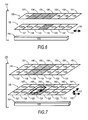
- oscillatory movement of a physical pixel array 120 is not limited to single pixel displacements.
- Figure 6 which substantially corresponds to the arrangement illustrated in Figure 3 , shows displacement of the physical pixel array 120 by three pixel elements.
- the target value of all pixel elements in Figure 6 is 100, with the single failed pixel having a gray level of 0.
- the shown displacement allows light from a single failed modulator to be spread among three pixels, decreasing the required intensification of the light intensity source 114 to bring the perceived level back to its target gray level value of 100.
- oscillatory pixel displacement can correspond to five, ten, or more columns (or rows) using suitable actuators and pixel arrays having a suitably high switching speed.
- oscillatory movement can be two dimensional.
- Figure 7 which substantially corresponds to the arrangement illustrated in Figure 3 , shows displacement of the physical pixel array 120 in two dimensions. Movement is by sequential and repeated column displacement of one pixel leftward, one row upward, one column rightward, and one row downward back to the original position. Again, the target value of all pixel elements is 100, with the single failed pixel having a gray level of 0.
- This two dimensional displacement allows light from a single failed modulator to be spread among four adjacent pixels, decreasing the required intensification of the light intensity source 114 to bring the perceived level back to its target gray level value of 100.
- oscillatory pixel displacement can be varied to have other oscillatory patterns.
- movement could be by sequential and repeated column displacement of ten pixels leftward, one row upward, ten columns rightward, and one row downward back to the original position, to provide a high aspect rectangular pixel displacement orbit (as compared to the square orbit of Figure 7 ).
- Other repeating patterns can of course be employed as desired.
- a light modulator failure compensation system 80 requires a light modulator failure identification unit 81 to identify malfunctioning light modulators (physical pixels in a one or two dimensional physical pixel array). Failure identification can be a one-time electronic or optical inspection at a manufacturing facility, or more preferably can be made "on the fly" during device warm-up or operation. Optical identification can be as simple as inspecting an array to see which element is anomalously bright (or dark). Electronic identification can rely on addressing each light modulator to switch optical states (gray levels) while simultaneously measuring capacitance, resistance, or any other suitable electrical switching response properties, with failures being identified by inappropriate electrical responses. For example, an electrostatically actuated micromirror held in a non-reflective state by stiction, damaged supports, or blocking debris would not report a normally expected capacitance change during switching, allowing it to be identified as a failed light modulator.
- the oscillatory pixel displacement unit 82 is utilized to distribute light from two or more physical pixels to each respective virtual pixel in a virtual pixel array seen by a viewer.
- the physical pixel array is moved by mechanical (as seen in Figures 4-7 ), optical (as seen in the following Figure 9 ) , or opto-mechanical techniques (as seen in the following Figure 10 ) that cause periodic displacement of the physical array of light.
- the extent, directionality, speed, and path of physical pixel array movement can be controlled by on-board or external digital or analog controllers, and can be optionally adjusted to provide for better image compensation. For example, a one dimensional movement of the physical pixel array with a two or three pixel movement shift may be initially adequate for light distribution. However, as additional light modulators fail, two dimensional movement at a higher speed may be required to provide adequate image quality.
- Positional and velocity information from the light modulator failure identification unit 81 and the oscillatory pixel displacement unit 82 is passed to image processing software or firmware in the image shift compensator 83.
- the software can be onboard (directly formed on the substrate as seen in Figure 1 ), or can be a separate memory and logic module (digital or analog) connected to the oscillatory pixel displacement unit and the electronics necessary for driving pixel image display.
- the compensator 83 is used to shift image position in coordination with periodic displacement of the oscillatory pixel displacement unit 82.
- the digital information used to provide a pixel image is periodically shifted one or more pixels in coordination with the movement of the physical array, so that two or more physical pixels together create a virtual pixel. For example, as each pixel was physically moved leftward two pixels, the pixel image display was moved rightward by two pixels, causing each virtual pixel to appear to remain unchanged (and unblurred), even though three physical pixels are actually providing light to a single virtual pixel.
- the image shift compensator 83 can optionally provide for subpixel display precision using various hyperacuity techniques.
- sub-pixel edge placement is enabled if specific light modulators are turned on not only while at integral pixel distance intervals, but for some amount of time while at a fractional distance from each integral pixel position.
- hyperacuity techniques based on timing can arbitrarily increase effective display resolution, and are particularly useful for minimizing aliasing features that are easily detected by human viewers.
- Image intensity rescaling unit 84 modifies some or all of the displayed gray levels of light modulators in the physical pixel array.
- the image intensity rescaling unit 84 controls this gray level adjustment, with those light modulators positioned adjacent to a failed light modulator generally having the greatest differential gray level adjustment, and/or requiring rapid switching of gray levels (depending on their physical pixel position relative to the virtual pixel).
- variable light source intensification unit 85 (corresponding to light source 50 of Figure 1 ). Compensation for loss of image brightness is possible by simply increasing brightness of the light source intensification unit 85. Such brightness correction is easier if a large number of physical pixels provide each virtual pixel, with a 2:1 physical to virtual pixel ratio (such as discussed in connection with Figures 2-5 ) requiring a doubling of light source brightness, while a 10:1 ratio only requires about a 10% increase in brightness to provide a fully corrected image 86.
- a variable light source intensification unit 85 may not be required to satisfy viewer expectations.
- an approximately corrected image 86 will be displayed, with brightness losses in the vicinity of failed pixel elements being imperceptible or at least not bothersome to a viewer.
- selective image display intensity adjustments in the region of the failed pixels with minimal or negligible corrections to far removed regions (for example, those regions positioned ten to a hundred pixels away from the failed pixel) are contemplated. Again, because of known limits to human visual perception, such limited compensation may provide adequate fault correction for viewers.
- the image shift compensator unit 83 can utilize information about the position and velocity of the effective array motion to determine the appropriate image shift and intensity corrections such as described in connection with Figure 8 .
- an implementation which utilizes oscillatory translation over a distance of 20 pixels may have uniform velocity in the centre of the oscillation, but will move slower at the endpoints.
- the image shift compensator can obtain information about the motion through position feedback, through velocity feedback, or through other means of prescribing motion, such as a constraining motion to be a function of time, and make corrections as necessary to display a deblurred image.
- Figure 9 illustrates a schematic, partially broken away view of a fault tolerant display system 210 in accordance with the present invention, which is capable of supporting mechanisms for mechanically or optically compensating for failed, defective, or intermittently operating pixels in a display.
- Figure 9 illustrates a mirror based reflective display 240 having row and column physical arrays 242 of pivotal mirrors 244 fixedly mounted to rotate with respect to a substrate 212.
- various other reflective or transmissive display devices including those discussed in connection with Figure 1 , can be used in the present invention.
- a virtual gray scale pixel array image 280 on a screen 282 can be produced by controlling the bistable position of each pivotal mirror 244 in the physical array 242, with each mirror selectively controlled to reflect incident light to an absorber (not shown) or allow its transmission to screen 282 via a pixel image displacement mirror 270 (pivotably mounted on an actuator 272) either directly or in conjunction with intervening projective optics, magnifiers, or fixed reflectors (not shown).
- an incident light beam 256 from light source 250 strikes the physical array 242 of light modulators, and is reflected in a desired image pattern toward mirror 270.
- the mirror 270 can be rotated (for example, at a 10Hz, 100HZ, 1000Hz, or greater frequency) by an actuator 272 to displace the beam by a distance corresponding to one or more virtual pixels of the virtual gray scale pixel array image 280.
- Operation of actuator 272 for pivoting the mirror in direction 274 can be enabled in either one, two, or three dimensions by electrostatic attraction, electromagnetic attraction, a piezovibrator, a movable linear stage, an angular arm, or any other conventional mechanism for periodically effecting rotation or movement of mirror 270.
- on-board control electronics 290 can be used for implementing various image processing module units previously described in connection with Figure 8 , including mirror fault identification, image rescaling, optional hyperacuity processing and control of mirror 270 for virtual pixel movement.
- Movement of mirror 270 is generally through a distance corresponding to integral multiples of each row or column distance in the virtual gray scale pixel array image 280.
- the mirror 270 can rotate a certain distance sufficient to allow each row 284 in the array 280 to occupy for a brief time the position of an adjacent row 286.
- full two dimensional movement pixel displacement is also possible.
- Figure 10 illustrates another embodiment of the present invention for fault tolerant correction of damaged physical pixel arrays.
- Fault tolerant display system 310 supports redundant arrays 385 mounted on substrate 312 for mechanically or optically compensating for failed, defective, or intermittently operating pixels in a display.
- System 310 includes a mirror based reflective display 340 having a row and column physical array 342 of pivotal mirrors 344 mounted for bistable rotation with respect to a substrate 312.
- the reflective display 340 is further mounted on a movable element 314, similar to that discussed in connection with Figure 1 , for supporting oscillatory movement of array 342.
- various other reflective or transmissive display devices including those discussed in connection with Figure 1 , can be used in the present invention.
- multiple redundant rows or columns are contemplated for operation of alternative embodiments of the present invention, with complete duplication of all rows or columns of physical array 342 being within the scope of the invention.
- a virtual gray scale pixel array image 380 on a screen 382 can be produced by controlling the bistable position of each pivotal mirror 344 in the physical array 342 of light modulators, with each mirror selectively controlled to reflect incident light to an absorber (not shown) or allow its transmission to screen 382 to provide a virtual pixel array image 380.
- incident light beam 356 from light source 350 striking the redundant array 385 of light modulators is ordinarily reflected away from the screen 382.
- the physical array 342 can be oscillated (by piezovibrator 314 in directions 316 and 318, for example) and subjected to various image processing techniques such as discussed in connection with Figure 8 to provide adequate fault correction.
- the foregoing described techniques may be unable to fully compensate for the faults.
- a mirror 370 can be rotated in direction 374 by actuator 372 to map the reflected beam from the redundant array 385 from its initial virtual position (rows 384) onto the position of failed virtual rows 386.
- operation of actuator 372 for pivoting the mirror can be enabled in either one, two, or three dimensions by electrostatic attraction, electromagnetic attraction, a piezovibrator, a movable linear stage, an angular arm, or any other conventional mechanism for periodically effecting rotation or movement of mirror 370.
- the mirror can be fixed in position to direct a virtual pixel image from redundant rows to overlap rows of failed pixels.
- large numbers of redundant rows including as many redundant rows as are present in the physical array 342, can be positioned beside the physical array.
- two highly defective physical arrays can be positioned to project an overlapping virtual array, with the second physical array turning on (when required) only those pixels that are positioned to replace failed pixels in the first physical array.
- Such an embodiment of the present invention allows two costly, yet defective, physical arrays to cooperate to emulate a non-defective array. Since failure rates currently approach 80% to 90% for many varieties of high pixel density physical arrays, the present invention of combining two defective physical arrays can be cost effective.
- overlapping virtual projections from redundant rows and the physical array can be employed in conjunction with an oscillatory fault compensation mechanism such as describe in connection with Figures 1-8 .
- the mirror 370 can be rotated in one or two dimensions to track oscillatory movement of the physical array, in a manner similar to that described in connection with Figure 9 . This allows large scale row defects to be completely compensated for by virtual projections of redundant arrays, while isolated pixel failures can be corrected for using oscillatory movement and image processing such as discussed in connection with Figures 1-8 .
- oscillatory movement allows for straightforward replacement of failed pixels on an array edge.
- the physical array can be surrounded by ten or twenty rows (or columns) of redundant arrays that are transiently moved into position to provide replacement virtual pixels.
Landscapes
- Engineering & Computer Science (AREA)
- Multimedia (AREA)
- Signal Processing (AREA)
- Physics & Mathematics (AREA)
- Computer Hardware Design (AREA)
- General Physics & Mathematics (AREA)
- Theoretical Computer Science (AREA)
- Mechanical Light Control Or Optical Switches (AREA)
- Control Of Indicators Other Than Cathode Ray Tubes (AREA)
Claims (9)
- Visualisierungssystem, das Folgendes umfasst:eine Lichtquelle (250),eine sichtbare Anzeigefläche (282),eine zweidimensionale Lichtmodulatoranordnung (242) mit mehreren Lichtmodulatoren (244), die in einer ersten Reihe und einer zweiten Reihe angeordnet sind, um Licht von der Lichtquelle (250) zu modulieren, wobei von der ersten Reihe moduliertes Licht als eine erste Reihe (284) von Pixeln auf der Anzeigefläche (282) präsentiert wird und von der zweiten Reihe moduliertes Licht als eine zweite Reihe (286) von Pixeln auf der Anzeigefläche (282) präsentiert wird, undwenigstens ein optisches Element (270), das so ausgelegt ist, dass es in einem ersten Zustand jeweils von der ersten und zweiten Reihe (284, 286) moduliertes Licht zur ersten bzw. zweiten Reihe auf der Anzeigefläche (282) leitet; und in einem zweiten Zustand das von der ersten Reihe (284) modulierte Licht zu der zweiten Reihe (286) auf der Anzeigefläche (282) leitet; wobei das wenigstens eine optische Element (270) zum periodischen Umschalten zwischen einem ersten und einem zweiten Zustand ausgelegt ist, um einen Ausfall in wenigstens einem der Lichtmodulatoren in der zweiten Reihe von Lichtmodulatoren (244) zu kompensieren.
- Visualisierungssystem nach Anspruch 1, wobei das wenigstens eine optische Element (270) ferner einen beweglichen Spiegel umfasst.
- Visualisierungssystem nach Anspruch 2, wobei der bewegliche Spiegel mit einer Frequenz von mehr als 10 Hz oszilliert wird.
- Visualisierungssystem nach Anspruch 1, 2 oder 3, wobei die mehreren Lichtmodulatoren (244) Licht regulierbar transmittieren und absorbieren.
- Visualisierungssystem nach Anspruch 1, 2 oder 3, wobei die mehreren Lichtmodulatoren (244) Licht reflektieren.
- Visualisierungssystem nach einem vorherigen Anspruch, wobei das wenigstens eine optische Element (270) Licht von der Anordnung (242) in einer Spaltenrichtung sowie in einer Reihenrichtung verschieben kann.
- Visualisierungssystem nach einem vorherigen Anspruch, wobei die Lichtquelle einen Lichtstrahl von variabler Intensität erzeugt und das System ferner ein Lichtmodulatorausfall-Kompensationssystem (80) zum Korrigieren bei Ausfall von wenigstens einem der mehreren Lichtmodulatoren (244) umfasst, wobei das Lichtmodulatorausfall-Kompensationssystem (80) ein Bildumskalierungsmodul (84) zum Variieren der scheinbaren Anzeigeintensität des Lichtmodulators und eine Lichtquellenintensitätsregelung (85) zum Erhöhen der Intensität des Lichtstrahls von variabler Intensität aufweist.
- Visualisierungssystem nach einem der Ansprüche 1 bis 6, wobei:die mehreren Lichtmodulatoren (244) ein erstes Bild definieren,das wenigstens eine optische Element (270) das erste Bild von der Lichtmodulatoranordnung (242) empfängt und ein zweites Bild projiziert, wobei das optische Element (270) so gesteuert wird, dass es das zweite Bild häufiger als alle 1/10 einer Sekunde periodisch verschiebt, undein Lichtmodulatorausfall-Kompensationssystem (80) zum Korrigieren bei Ausfall von wenigstens einem der mehreren Lichtmodulatoren (242), wobei das Lichtmodulatorausfall-Kompensationssystem (80) ein Bildschiebemodul (83) zum Umdefinieren des ersten Bildes in Koordination mit einer periodischen Verschiebung des zweiten Bildes und ein Umskalierungsmodul (84) zum Reduzieren der scheinbaren Anzeigeintensität des Lichtmodulators für wenigstens einige Lichtmodulatoren (28, 44) aufweist, die neben einem ausgefallenen Lichtmodulator positioniert sind.
- Visualisierungssystem nach Anspruch 8, das ferner eine Lichtquelle (250) von variabler Intensität zum Erhöhen der Lichtintensität zum Kompensieren einer reduzierten scheinbaren Anzeigeintensität des Lichtmodulators umfasst.
Applications Claiming Priority (2)
| Application Number | Priority Date | Filing Date | Title |
|---|---|---|---|
| US08/884,364 US5790297A (en) | 1997-06-26 | 1997-06-26 | Optical row displacement for a fault tolerant projective display |
| US884364 | 1997-06-26 |
Publications (3)
| Publication Number | Publication Date |
|---|---|
| EP0887689A2 EP0887689A2 (de) | 1998-12-30 |
| EP0887689A3 EP0887689A3 (de) | 2000-02-23 |
| EP0887689B1 true EP0887689B1 (de) | 2014-12-17 |
Family
ID=25384458
Family Applications (1)
| Application Number | Title | Priority Date | Filing Date |
|---|---|---|---|
| EP98303737.5A Expired - Lifetime EP0887689B1 (de) | 1997-06-26 | 1998-05-13 | System zur optischen Zeilenverschiebung für eine fehlertolerante Projektionsanzeigevorrichtung |
Country Status (2)
| Country | Link |
|---|---|
| US (1) | US5790297A (de) |
| EP (1) | EP0887689B1 (de) |
Families Citing this family (23)
| Publication number | Priority date | Publication date | Assignee | Title |
|---|---|---|---|---|
| US6985127B1 (en) * | 1994-09-01 | 2006-01-10 | The United States Of America As Represented By The Secretary Of The Navy | Programmable gray-scale liquid crystal display |
| US6028690A (en) * | 1997-11-26 | 2000-02-22 | Texas Instruments Incorporated | Reduced micromirror mirror gaps for improved contrast ratio |
| SE9800665D0 (sv) * | 1998-03-02 | 1998-03-02 | Micronic Laser Systems Ab | Improved method for projection printing using a micromirror SLM |
| DE69909136T2 (de) * | 1998-10-12 | 2004-05-06 | Dicon A/S | Rapid-prototyping-vorrichtung und rapid-prototyping-methode |
| US6642964B1 (en) * | 1998-12-15 | 2003-11-04 | Xerox Corporation | Geometric configurations for photosites for reducing moire patterns |
| US7030894B2 (en) * | 2002-08-07 | 2006-04-18 | Hewlett-Packard Development Company, L.P. | Image display system and method |
| US6963319B2 (en) * | 2002-08-07 | 2005-11-08 | Hewlett-Packard Development Company, L.P. | Image display system and method |
| US7034811B2 (en) | 2002-08-07 | 2006-04-25 | Hewlett-Packard Development Company, L.P. | Image display system and method |
| US7993108B2 (en) | 2002-10-09 | 2011-08-09 | Abbott Diabetes Care Inc. | Variable volume, shape memory actuated insulin dispensing pump |
| US7727181B2 (en) * | 2002-10-09 | 2010-06-01 | Abbott Diabetes Care Inc. | Fluid delivery device with autocalibration |
| CA2501825C (en) | 2002-10-09 | 2009-12-01 | Therasense, Inc. | Fluid delivery device, system and method |
| US7679407B2 (en) | 2003-04-28 | 2010-03-16 | Abbott Diabetes Care Inc. | Method and apparatus for providing peak detection circuitry for data communication systems |
| AU2006226988B2 (en) | 2005-03-21 | 2011-12-01 | Abbott Diabetes Care, Inc. | Method and system for providing integrated medication infusion and analyte monitoring system |
| US7768408B2 (en) | 2005-05-17 | 2010-08-03 | Abbott Diabetes Care Inc. | Method and system for providing data management in data monitoring system |
| US7620437B2 (en) | 2005-06-03 | 2009-11-17 | Abbott Diabetes Care Inc. | Method and apparatus for providing rechargeable power in data monitoring and management systems |
| US7756561B2 (en) | 2005-09-30 | 2010-07-13 | Abbott Diabetes Care Inc. | Method and apparatus for providing rechargeable power in data monitoring and management systems |
| US7583190B2 (en) | 2005-10-31 | 2009-09-01 | Abbott Diabetes Care Inc. | Method and apparatus for providing data communication in data monitoring and management systems |
| US8344966B2 (en) | 2006-01-31 | 2013-01-01 | Abbott Diabetes Care Inc. | Method and system for providing a fault tolerant display unit in an electronic device |
| US8579853B2 (en) | 2006-10-31 | 2013-11-12 | Abbott Diabetes Care Inc. | Infusion devices and methods |
| US8560082B2 (en) | 2009-01-30 | 2013-10-15 | Abbott Diabetes Care Inc. | Computerized determination of insulin pump therapy parameters using real time and retrospective data processing |
| WO2010129375A1 (en) | 2009-04-28 | 2010-11-11 | Abbott Diabetes Care Inc. | Closed loop blood glucose control algorithm analysis |
| FI3936032T3 (fi) | 2009-07-23 | 2024-08-14 | Abbott Diabetes Care Inc | Glukoositasojen fysiologiseen säätelyyn liittyvien tietojen reaaliaikainen hallinta |
| US9135893B2 (en) | 2013-05-28 | 2015-09-15 | Infineon Technologies Ag | Display device |
Family Cites Families (16)
| Publication number | Priority date | Publication date | Assignee | Title |
|---|---|---|---|---|
| US4615595A (en) * | 1984-10-10 | 1986-10-07 | Texas Instruments Incorporated | Frame addressed spatial light modulator |
| GB9008032D0 (en) * | 1990-04-09 | 1990-06-06 | Rank Brimar Ltd | Video display systems |
| EP0460890A3 (en) * | 1990-06-06 | 1992-11-25 | Texas Instruments Incorporated | Optical tracking system |
| JPH04194814A (ja) * | 1990-11-22 | 1992-07-14 | Minolta Camera Co Ltd | 光ビーム走査光学系 |
| CA2081753C (en) * | 1991-11-22 | 2002-08-06 | Jeffrey B. Sampsell | Dmd scanner |
| US5231388A (en) * | 1991-12-17 | 1993-07-27 | Texas Instruments Incorporated | Color display system using spatial light modulators |
| JPH05313118A (ja) * | 1992-05-14 | 1993-11-26 | Kodo Eizo Gijutsu Kenkyusho:Kk | 画像表示装置 |
| JP3318904B2 (ja) * | 1993-07-14 | 2002-08-26 | テキサス インスツルメンツ インコーポレイテツド | プロジエクタ装置 |
| US5526172A (en) * | 1993-07-27 | 1996-06-11 | Texas Instruments Incorporated | Microminiature, monolithic, variable electrical signal processor and apparatus including same |
| US5517347A (en) * | 1993-12-01 | 1996-05-14 | Texas Instruments Incorporated | Direct view deformable mirror device |
| US5619223A (en) * | 1994-04-14 | 1997-04-08 | Prime View Hk Limited | Apparatus for increasing the effective yield of displays with integregated row select driver circuit |
| US5504504A (en) * | 1994-07-13 | 1996-04-02 | Texas Instruments Incorporated | Method of reducing the visual impact of defects present in a spatial light modulator display |
| US5490009A (en) * | 1994-10-31 | 1996-02-06 | Texas Instruments Incorporated | Enhanced resolution for digital micro-mirror displays |
| US5592188A (en) * | 1995-01-04 | 1997-01-07 | Texas Instruments Incorporated | Method and system for accentuating intense white display areas in sequential DMD video systems |
| US5612713A (en) * | 1995-01-06 | 1997-03-18 | Texas Instruments Incorporated | Digital micro-mirror device with block data loading |
| US5535047A (en) | 1995-04-18 | 1996-07-09 | Texas Instruments Incorporated | Active yoke hidden hinge digital micromirror device |
-
1997
- 1997-06-26 US US08/884,364 patent/US5790297A/en not_active Expired - Lifetime
-
1998
- 1998-05-13 EP EP98303737.5A patent/EP0887689B1/de not_active Expired - Lifetime
Also Published As
| Publication number | Publication date |
|---|---|
| EP0887689A3 (de) | 2000-02-23 |
| US5790297A (en) | 1998-08-04 |
| EP0887689A2 (de) | 1998-12-30 |
Similar Documents
| Publication | Publication Date | Title |
|---|---|---|
| EP0887681B1 (de) | Fehler-unempfindliche Projektions-Anzeige mit redundanten Lichtmodulatoren | |
| EP0887690B1 (de) | Fehlertolerantes Anzeigesystem mit Lichtmodulator | |
| EP0887689B1 (de) | System zur optischen Zeilenverschiebung für eine fehlertolerante Projektionsanzeigevorrichtung | |
| KR100346879B1 (ko) | 결함의시각적영향을감소시키는방법및디스플레이장치 | |
| TWI778098B (zh) | 掃描顯示裝置的發光結構 | |
| US5805119A (en) | Vehicle projected display using deformable mirror device | |
| US5457493A (en) | Digital micro-mirror based image simulation system | |
| EP0665458B1 (de) | DMD-Struktur mit erhöhtem horizontalen Auflösungsvermögen | |
| EP0657760A1 (de) | Bildsimulations- und Projektionssystem | |
| JP5402791B2 (ja) | プロジェクター | |
| JP6859990B2 (ja) | 電気光学装置及びその制御方法 | |
| WO2008024280A2 (en) | An image display system having adjustable intensities | |
| US7330298B2 (en) | Optical system and method for increasing image resolution and/or dithering in projection applications | |
| US8567956B2 (en) | Projector | |
| JP2008039795A (ja) | マルチディスプレイシステム | |
| JP4346125B2 (ja) | ディスプレイシステム | |
| JP5059446B2 (ja) | 表示装置、投射型表示装置、光路シフト素子の制御回路および光路シフト素子 | |
| JP4077139B2 (ja) | 画像表示装置 | |
| KR100640872B1 (ko) | 투사표시장치 | |
| US20060176362A1 (en) | Optical system and method for increasing image resolution and/or dithering in printing applications | |
| US20080055340A1 (en) | Display apparatus including optical modulator and image controlling method | |
| JP4430647B2 (ja) | 画像表示装置 | |
| JP2002357809A (ja) | 画像表示装置 | |
| CN117666123A (zh) | 像源组件、显示装置和交通工具 | |
| KR102149535B1 (ko) | 디지털 노광기 |
Legal Events
| Date | Code | Title | Description |
|---|---|---|---|
| PUAI | Public reference made under article 153(3) epc to a published international application that has entered the european phase |
Free format text: ORIGINAL CODE: 0009012 |
|
| AK | Designated contracting states |
Kind code of ref document: A2 Designated state(s): DE FR GB |
|
| AX | Request for extension of the european patent |
Free format text: AL;LT;LV;MK;RO;SI |
|
| PUAL | Search report despatched |
Free format text: ORIGINAL CODE: 0009013 |
|
| AK | Designated contracting states |
Kind code of ref document: A3 Designated state(s): AT BE CH CY DE DK ES FI FR GB GR IE IT LI LU MC NL PT SE |
|
| AX | Request for extension of the european patent |
Free format text: AL;LT;LV;MK;RO;SI |
|
| RIC1 | Information provided on ipc code assigned before grant |
Free format text: 7G 02F 1/13 A, 7G 02B 26/08 B, 7H 04N 9/31 B |
|
| 17P | Request for examination filed |
Effective date: 20000823 |
|
| AKX | Designation fees paid |
Free format text: DE FR GB |
|
| 17Q | First examination report despatched |
Effective date: 20070222 |
|
| GRAP | Despatch of communication of intention to grant a patent |
Free format text: ORIGINAL CODE: EPIDOSNIGR1 |
|
| INTG | Intention to grant announced |
Effective date: 20140704 |
|
| GRAS | Grant fee paid |
Free format text: ORIGINAL CODE: EPIDOSNIGR3 |
|
| GRAA | (expected) grant |
Free format text: ORIGINAL CODE: 0009210 |
|
| AK | Designated contracting states |
Kind code of ref document: B1 Designated state(s): DE FR GB |
|
| REG | Reference to a national code |
Ref country code: GB Ref legal event code: FG4D |
|
| REG | Reference to a national code |
Ref country code: DE Ref legal event code: R096 Ref document number: 69843338 Country of ref document: DE Effective date: 20150129 |
|
| REG | Reference to a national code |
Ref country code: FR Ref legal event code: PLFP Year of fee payment: 18 |
|
| REG | Reference to a national code |
Ref country code: DE Ref legal event code: R097 Ref document number: 69843338 Country of ref document: DE |
|
| PLBE | No opposition filed within time limit |
Free format text: ORIGINAL CODE: 0009261 |
|
| STAA | Information on the status of an ep patent application or granted ep patent |
Free format text: STATUS: NO OPPOSITION FILED WITHIN TIME LIMIT |
|
| 26N | No opposition filed |
Effective date: 20150918 |
|
| REG | Reference to a national code |
Ref country code: FR Ref legal event code: PLFP Year of fee payment: 19 |
|
| PGFP | Annual fee paid to national office [announced via postgrant information from national office to epo] |
Ref country code: DE Payment date: 20160421 Year of fee payment: 19 Ref country code: GB Payment date: 20160426 Year of fee payment: 19 |
|
| PGFP | Annual fee paid to national office [announced via postgrant information from national office to epo] |
Ref country code: FR Payment date: 20160422 Year of fee payment: 19 |
|
| REG | Reference to a national code |
Ref country code: DE Ref legal event code: R119 Ref document number: 69843338 Country of ref document: DE |
|
| GBPC | Gb: european patent ceased through non-payment of renewal fee |
Effective date: 20170513 |
|
| REG | Reference to a national code |
Ref country code: FR Ref legal event code: ST Effective date: 20180131 |
|
| PG25 | Lapsed in a contracting state [announced via postgrant information from national office to epo] |
Ref country code: DE Free format text: LAPSE BECAUSE OF NON-PAYMENT OF DUE FEES Effective date: 20171201 Ref country code: GB Free format text: LAPSE BECAUSE OF NON-PAYMENT OF DUE FEES Effective date: 20170513 |
|
| PG25 | Lapsed in a contracting state [announced via postgrant information from national office to epo] |
Ref country code: FR Free format text: LAPSE BECAUSE OF NON-PAYMENT OF DUE FEES Effective date: 20170531 |